Table of Contents
Advertisement
Quick Links
AN_1811_PL52_1811_234307
CoolGaN™ 600 V half-bridge evaluation
platform featuring GaN EiceDRIVER™
About this document
Authors: Eric Persson, Yalcin Haksoz
Ordering code: EVAL_1EDF_G1B_HB_GAN
Scope and purpose
This application note explains how to setup and use the CoolGaN™ 600 V half-bridge evaluation board. The
board features a half-bridge of 70 mΩ GaN power transistors, a pair of EiceDRIVER™ GaN gate drivers, and
isolated power supplies for the gate drivers along with input logic that provides adjustable deadtime. Using an
external inductor, the board can be configured for buck or boost-mode, double-pulse testing or continuous
PWM operation, hard or soft-switching at power levels to several kW and frequencies up to MHz range.
Intended audience
This document is intended for power electronic engineers and designers who are already familiar with MOSFET
or IGBT-based converters, inverters and gate drivers, who are interested in looking at the similarities and
differences of GaN power transistors compared to their silicon counterparts.
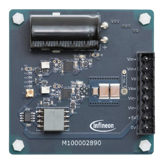
Figure 1
Front and back view of the CoolGaN™ half-bridge evaluation platform
Application Note
Please read the Important Notice and Warnings at the end of this document
V 1.1
www.infineon.com/eval-1edf-g1b-hb-gan
page 1 of 23
2020-11-09
Advertisement
Table of Contents

Related Manuals for Infineon CoolGaN


Summary of Contents for Infineon CoolGaN
-
Page 1: About This Document
Ordering code: EVAL_1EDF_G1B_HB_GAN Scope and purpose This application note explains how to setup and use the CoolGaN™ 600 V half-bridge evaluation board. The board features a half-bridge of 70 mΩ GaN power transistors, a pair of EiceDRIVER™ GaN gate drivers, and isolated power supplies for the gate drivers along with input logic that provides adjustable deadtime. -
Page 2: Table Of Contents
CoolGaN™ 600 V half-bridge evaluation platform featuring GaN EiceDRIVER™ Table of contents Table of contents About this document ........................1 Table of contents ..........................2 Introduction .......................... 3 Evaluation board specifications ......................3 Functional description ......................4 Circuit description ........................5 Input Logic and deadtime generator ...................... -
Page 3: Introduction
Introduction Introduction This 600 V gallium nitride (GaN) half-bridge evaluation board enables easy, rapid setup and test of CoolGaN™ transistors along with the dedicated GaN EiceDRIVER™ isolated gate driver IC. The generic topology is configurable for boost or buck operation, pulse testing or continuous full-power operation. Test points provide easy access to connect signals to an oscilloscope for measuring the switching performance of CoolGaN™... -
Page 4: Functional Description
CoolGaN™ 600 V half-bridge evaluation platform featuring GaN EiceDRIVER™ Functional description Functional description A typical block diagram is shown in Figure 2 for a double-pulse test application setup. A 5 V power supply provides the circuit power, and a 0-400 V power supply provides the DC bus voltage. The input PWM signal is provided by a lab pulse generator. -
Page 5: Circuit Description
130 ns (minus the 100 ns deadtime as described above). Any input pulse width shorter than this is not recommended, as the resulting output pulse is so small it is really no longer effective. For extremely short output pulse widths, contact your local Infineon applications support team to discuss gate drive circuit optimization for the specific requirement. -
Page 6: Isolated Gate Driver Power Supply
CoolGaN™ 600 V half-bridge evaluation platform featuring GaN EiceDRIVER™ Circuit description The TNEG pins of U1 and U2 are connected to timing resistors R13 and R23 respectively. These resistors program the duration of the negative off voltage as explained in section 3.7 of the 1EDF5673K datasheet. -
Page 7: Gate Drive Circuit
(OUTG) connected to the CoolGaN™ gate, and the other (OUTS) connected to the CoolGaN™ Kelvin source. VDDx is bypassed to VSSx with a 100 nF capacitor Cx3. The gate RC network described in the datasheet consists of Rx4, Cx4 and Rx5. The small Schottky diode Dx5 provides a low-impedance return-path for faster gate turnoff, effectively bypassing Rx4. -
Page 8: Half-Bridge Output Circuit
CoolGaN™ 600 V half-bridge evaluation platform featuring GaN EiceDRIVER™ Circuit description Half-bridge output circuit GaN transistors Q1 and Q2 form the high and low-side transistors of the half-bridge, as shown in Figure 7. The drain of Q1 is connected to the DC bus (V ). -
Page 9: Setup And Use
CoolGaN™ 600 V half-bridge evaluation platform featuring GaN EiceDRIVER™ Setup and use Setup and use Attention: This evaluation board has exposed high-voltage contacts. Use appropriate protective measures to avoid shock. The evaluation board has no overcurrent shutdown, so it is possible to drive the GaN transistors to currents far beyond their rating, which may result in their destruction. -
Page 10: Connections For Double-Pulse Testing
CoolGaN™ 600 V half-bridge evaluation platform featuring GaN EiceDRIVER™ Setup and use Figure 8 Typical test setup – example is shown for pulse testing 4.2.1 Connections for double-pulse testing Refer back to Figure 2 for the proper setup and connections for double-pulse testing. Note that the single terminal block X1 has all 6 output power connections, plus the 5 V DC supply connections. - Page 11 CoolGaN™ 600 V half-bridge evaluation platform featuring GaN EiceDRIVER™ Setup and use Evaluation Board Vin+ 0-400 V DC Deadtime Isolated Gate Test Laboratory Circuit Driver Circuit Inductor Power Supply 50Ω Pulse Generator Deadtime Isolated Gate Circuit Driver Circuit Load 5 V DC...
-
Page 12: Connections For Boost Topology
CoolGaN™ 600 V half-bridge evaluation platform featuring GaN EiceDRIVER™ Setup and use Note that the slew-rate of V (TP3) is asymmetrical: this is because the rising-edge is driven by the -4 A inductor peak current, but the falling-edge is driven by the +9.5 A peak current, more than 2X larger current. The commutating slew-rate is directly proportional to the peak inductor current based on I=C dv/dt where I is the inductor current, and C is the total switch-node capacitance. -
Page 13: Input Pwm Generator Connections And Settings
CoolGaN™ 600 V half-bridge evaluation platform featuring GaN EiceDRIVER™ Setup and use Input PWM generator connections and settings The PWM input is the logic command to the half-bridge output: when the PWM input is high, the half-bridge output V is at its high state (connected to the V bus). -
Page 14: Verifying And Adjusting Deadtime
CoolGaN™ 600 V half-bridge evaluation platform featuring GaN EiceDRIVER™ Setup and use limited to 0.2 A because the on-board bus capacitors will provide the peak current (for low-value inductors <100 µH). Verifying and adjusting deadtime The evaluation board has two independent deadtime adjustments. When the PWM input goes high, the low side gate driver turns off and then the high-side gate driver turns on after the rising-edge deadtime. -
Page 15: Test Inductor Recommendation
CoolGaN™ 600 V half-bridge evaluation platform featuring GaN EiceDRIVER™ Setup and use Apply power to the board and trigger on the rising edge of TP4. You should have a signal that looks similar to Figure 12. The cursors assume that turn-off is complete when TP2 crosses 0 V, and turn-on is assumed to begin when TP1 reaches about 2.5 V. -
Page 16: Initial Checkout
CoolGaN™ 600 V half-bridge evaluation platform featuring GaN EiceDRIVER™ Setup and use Initial checkout Assuming the board is already setup per section 4.6, the next step is to add an external inductor and bring-up the DC bus to operate at the desired test condition. This example shows how to setup the board for double- pulse testing. -
Page 17: Operation At High Power Levels
CoolGaN™ 600 V half-bridge evaluation platform featuring GaN EiceDRIVER™ Setup and use Note: The HV supply should always be the last thin to turn-on, and the first thing to turn-off when measurement is completed. Start with a low-voltage on the DC bus – 25 V just to make sure that everyting is connected properly, and that the current is ramping-up as expected, the current probe polarity is correct, etc. -
Page 18: Complete Schematic
CoolGaN™ 600 V half-bridge evaluation platform featuring GaN EiceDRIVER™ Complete schematic Complete schematic Note: Part numbers 1-9 are in the ouput power stage. 1x part numbers belong to the high-side gate drive, 2x are low-side gate drive, and 3x are input ground connected. -
Page 19: Pcb Layout
CoolGaN™ 600 V half-bridge evaluation platform featuring GaN EiceDRIVER™ PCB layout PCB layout The evaluation board is 1.6 mm thick, with 4 evenly-spaced copper layers 35 µm thick. The layer stackup is depicted below. Figure 16 Top layer copper layer with top component overlay... - Page 20 CoolGaN™ 600 V half-bridge evaluation platform featuring GaN EiceDRIVER™ PCB layout Figure 18 Lower middle copper layer with top and bottom component overlay Figure 19 Bottom copper layer with bottom component overlay (viewed from top) Application Note 20 of 23 V 1.1...
-
Page 21: Bill Of Materials
CoolGaN™ 600 V half-bridge evaluation platform featuring GaN EiceDRIVER™ Bill of materials Bill of materials The following table describes all of the components on the PCB: Table 3 PCB BOM Designator Description CAP ALUM 100UF 20% 450V 18D 35L 7.5P... -
Page 22: Revision History
CoolGaN™ 600 V half-bridge evaluation platform featuring GaN EiceDRIVER™ Revision history Revision history Document Date of release Description of changes version V 1.0 2019-01-16 First release V 1.1 2020-11-09 Updates for version ‘B’ of the driver IC – updated shcematics, BOM and PCB images, and minor modifications about the Tneg pin connections in section 3.1... - Page 23 Infineon Technologies hereby disclaims dangerous substances. For information on the types © 2020 Infineon Technologies AG. any and all warranties and liabilities of any kind in question please contact your nearest Infineon All Rights Reserved. (including without limitation warranties of non- Technologies office.
Need help?
Do you have a question about the CoolGaN and is the answer not in the manual?
Questions and answers