
Related Manuals for MICROENER MC3V-X/10-4


Summary of Contents for MICROENER MC3V-X/10-4
- Page 1 MC3V-X/10-4 MO-0355-ING Doc. N° THREE PHASE Over/Under VOLTAGE Over/Under FREQUENCY MICROPROCESSOR RELAY TYPE MC3V-X/10-4 (I/O Boards) OPERATION MANUAL 06.01.2011 Microener - Copyright 2011 FW 940.09.01.x Date Rev.
-
Page 2: Table Of Contents
16. CONNECTION DIAGRAM ________________________________________________________________________________________ 29 17. OVERALL DIMENSIONS ________________________________________________________________________________________ 30 18. DIRECTION FOR PCB'S DRAW-OUT AND PLUG-IN __________________________________________________________________ 31 18.1 - Draw-Out _________________________________________________________________________________________________ 31 18.2 - Plug-In ___________________________________________________________________________________________________ 31 19. ELECTRICAL CHARACTERISTICS ________________________________________________________________________________ 32 06.01.2011 Microener - Copyright 2011 FW 940.09.01.x Date Rev. Pag. -
Page 3: General Utilization And Commissioning Directions
The electronic circuits reduced by M.S. are completely safe from electrostatic discharge (8 KV IEC 255.22.2) when housed in their case; withdrawing the modules without proper cautions expose them to the risk of damage. 06.01.2011 Microener - Copyright 2011 FW 940.09.01.x Date Rev. -
Page 4: Maintenance
Internal calibrations and components should not be altered or replaced. For repair please ask the Manufacturer or its authorised Dealers. Misapplication of the above warnings and instruction relieves the Manufacturer of any liability. 06.01.2011 Microener - Copyright 2011 FW 940.09.01.x Date Rev. -
Page 5: General Characteristics
80V(-20%) / 220V(+15%) a.c. a) - b) - 24V(-20%) / 125V(+20%) d.c. 90V(-20%) / 250V(+20%) d.c. Before energising the unit check that supply voltage is within the allowed limits. 06.01.2011 Microener - Copyright 2011 FW 940.09.01.x Date Rev. Pag. -
Page 6: Operation And Algorithms
Input voltages are supplied to 3 internal adapting transformers; the rated input voltage (phase-to- phase) can be programmed in the range (50 - 400)V. The display shows the measurement of the phase-to-neutral voltages in primary volt according to the programmed reference input values. 06.01.2011 Microener - Copyright 2011 FW 940.09.01.x Date Rev. Pag. -
Page 7: Functions And Settings (Function)
If disable the function is disactivated Operation controlled by Blocking Digital Input Function operation triggers the oscillographic wave form capture (see § Oscillographic) V>> Trip level of overvoltage protection Trip time delay tV>> 06.01.2011 Microener - Copyright 2011 FW 940.09.01.x Date Rev. Pag. -
Page 8: V< (1F27) - First Undervoltage Protection Level (Smallest Of 3 Phase-To-Neutral Voltages)
If disable the function is disactivated Operation controlled by Blocking Digital Input Function operation triggers the oscillographic wave form capture (see § Oscillographic) V<< Trip level of undervoltage protection tV<< Trip time delay 06.01.2011 Microener - Copyright 2011 FW 940.09.01.x Date Rev. Pag. -
Page 9: F> (F81) - Overfrequency Protection Level
If disable the function is disactivated Operation controlled by Blocking Digital Input Function operation triggers the oscillographic wave form capture (see § Oscillographic) Vo> Trip level of zero sequence overvoltage protection tVo> Trip time delay 06.01.20118 Rev. Microener - Copyright 2011 FW 940.09.01.x Date Pag. -
Page 10: V1< (F27V1) - Positive Sequence Undervoltage Protection Level
If disable the function is disactivated Operation controlled by Blocking Digital Input Function operation triggers the oscillographic wave form capture (see § Oscillographic) V2> Trip level of negative sequence overvoltage protection tV2> Trip time delay 06.01.2011 Microener - Copyright 2011 FW 940.09.01.x Date Rev. Pag. -
Page 11: Rtd - Remote Trip
The variable “ Opz “ can be programmed to trip the output relays same as the other protection functions (Opz = TRIP), or to only operate the “ IRF “ signal led without tripping the output relays (Opz = NoTRIP). 06.01.2011 Microener - Copyright 2011 FW 940.09.01.x Date Rev. -
Page 12: Osc - Oscillographic Recording
In any case the number of event stored can not exceed ten (10 x 0.3 sec). Any new event beyond the 3 sec capacity of the memory, cancel and overwrites the former records (FIFO Memory). 06.01.2011 Microener - Copyright 2011 FW 940.09.01.x Date Rev. -
Page 13: Comm - Communication Parameters
→ No Param No Parameters Timers → No Param No Parameters Buzzer “Beep” on operation of Keyboard buttons. LCD Backlight continuously “ON” or switched-on Automatically on operation of Keyboard buttons. 06.01.2011 Microener - Copyright 2011 FW 940.09.01.x Date Rev. Pag. -
Page 14: Instantaneous Output And Blocking Input
Moreover, the operation of each of the output relays can be programmed to be either Normally Deenergized (energized on tripping of the controlling Functional Element) or Normally Energized (Deenergized on tripping of the controlling Functional Element). 06.01.2011 Microener - Copyright 2011 FW 940.09.01.x Date Rev. -
Page 15: Digital Inputs
“ Last Trip “ and the I.R.F. signal led is set to flashing. If “ I.R.F. “ is programmed to “NO Trip”, and only the I.R.F. signal led is set to flashing. 06.01.2011 Microener - Copyright 2011 FW 940.09.01.x Date Rev. -
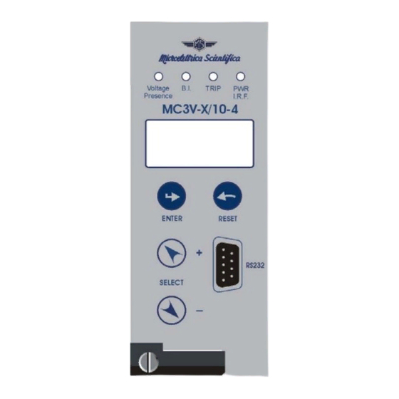
Page 16: Relay Management
LCD display, or remotely via the communication bus RS485 connected to the rear terminal blocks. The 2 line x 8 characters LCD display shows the available information. Key buttons operate according to the flow-chart herebelow. 06.01.2011 Microener - Copyright 2011 FW 940.09.01.x Date Rev. -
Page 17: Signalizations
Give access to any menu or convalidate any programming changement. Reset Return from the actual selected menu to the former menu. Select + Scrolls variables available in the different menus or increases/decreases setting values. Select - 06.01.2011 Microener - Copyright 2011 FW 940.09.01.x Date Rev. Pag. -
Page 18: Serial Communication Port
Maximum length of the serial bus can be up to 200m. For longer distance and for connection of up to 250 Relays, optical interconnection is recommend. (please ask Microelettrica for accessories) 06.01.2011 Microener - Copyright 2011 FW 940.09.01.x Date Rev. -
Page 19: Communication Port On Front Face Panel
This port is used for communication through the Front Face Panel between a local Lap-top PC. The physical link is RS232 by the standard female 9-pin D-sub connector available on the Front Face Panel. Via this Port complete Relay management and data acquisition is possible. 06.01.2011 Microener - Copyright 2011 FW 940.09.01.x Date Rev. -
Page 20: Menu And Variables
Number of External Trip commands V2> 0 – 65535 Number of Negative sequence overvoltage (time delayed) trip I.R.F. 0 – 65535 Number of Internal Relay Faults 0 – 65535 Number of HW recovery operations 06.01.2011 Microener - Copyright 2011 FW 940.09.01.x Date Rev. Pag. -
Page 21: Lasttrip (Event Recording)
% of rated system voltage V2> = 0 - 999999 % of rated system voltage to go back to “ Rec # “, to go back to “ Real Time Meas “. 06.01.2011 Microener - Copyright 2011 FW 940.09.01.x Date Rev. Pag. -
Page 22: R/W Set (Programming / Reading The Relay Settings)
Setting Range Step Unit Rated Primary voltage of phase V.T. 0.05 - 500 0.01 Rated Secondary voltage of phase V.T. 50 - 400 0.01 Freq System rated frequency 50 - 06.01.2011 Microener - Copyright 2011 FW 940.09.01.x Date Rev. Pag. -
Page 23: Function (Functions)
Function operation triggers the oscillographic wave Enable/Disable form capture TripLev → f< 40.50 Trip level of underfrequency protection 40 – 70 0.01 → Timers tf< 1.00 Trip time delay 0.05 – 60.00 0.01 06.01.2011 Microener - Copyright 2011 FW 940.09.01.x Date Rev. Pag. - Page 24 ON - OFF Automatically on operation of Keyboard buttons. TripLev → No Param. No Parameters → Timers No Param. No Parameters Settings can also be programmed via the serial communication ports. 06.01.2011 Microener - Copyright 2011 FW 940.09.01.x Date Rev. Pag.
-
Page 25: Relaycfg (Relay Configuration)
- Vo> - tVo> - V1< - tV1< - V2> - tV2> - RTD - IRF - HwRecov. 1.D1, 1.D2, 1.D3, 1.D4, 1.D5, 1.D6, 1.D7, 1.D8, 1.D9, 1.D10, Canstatus. → OpMode N.E. N.D. (Normally Deenergized) N.D./N.E. N.E. (Normally Energized) 06.01.2011 Microener - Copyright 2011 FW 940.09.01.x Date Rev. Pag. -
Page 26: Commands
“ Info/Ver “, “ Model XXXXXX ”, Model Relay “ RelayVrs ###.#.#X “, Firmware Version to go back to “ Info&Ver “. to go back to “ Real Time Meas “ 06.01.2011 Microener - Copyright 2011 FW 940.09.01.x Date Rev. Pag. -
Page 27: Keyboard Operational Diagram
MC3V-X/10-4 MO-0355-ING Doc. N° 12. Keyboard Operational Diagram 06.01.2011 Microener - Copyright 2011 FW 940.09.01.x Date Rev. Pag. -
Page 28: Password
This is extremely important as discharges eventually tacking place in other parts or components of the board can severely damage the relays or cause damages not immediately evident to the electronic components. 06.01.2011 Microener - Copyright 2011 FW 940.09.01.x Date Rev. -
Page 29: Connection Diagram
MC3V-X/10-4 MO-0355-ING Doc. N° 16. Connection Diagram 16.1 – UX10-4 - Expansion Module - Wiring Diagram (10 Digital Inputs + 4 Output Relays) 06.01.2011 Microener - Copyright 2011 FW 940.09.01.x Date Rev. Pag. -
Page 30: Overall Dimensions
MC3V-X/10-4 MO-0355-ING Doc. N° 17. Overall Dimensions PROTECTION DEGREE IP44 (IP54 on request) 06.01.2011 Microener - Copyright 2011 FW 940.09.01.x Date Rev. Pag. -
Page 31: Direction For Pcb's Draw-Out And Plug-In
Slide-in the card on the rails provided inside the enclosure. Plug-in the card completely and by pressing the handle to the closed position. Rotate anticlockwise the screws with the mark in the vertical position (locked). 06.01.2011 Microener - Copyright 2011 FW 940.09.01.x Date Rev. Pag. -
Page 32: Electrical Characteristics
9600 - 19200 - 38400 - 57600 – 8,N,1 – Modbus RTU The performances and the characteristics reported in this manual are not binding and can modified at any moment without notice 06.01.2011 Microener - Copyright 2011 FW 940.09.01.x Date Rev.
Need help?
Do you have a question about the MC3V-X/10-4 and is the answer not in the manual?
Questions and answers