Table of Contents
Advertisement
Quick Links
RE01 Group
16
32
Evaluation Kit RE01 256KB (EK-RE01 256KB)
User's Manual
RE Family/RE0 Series
All information contained in these materials, including products and product specifications,
represents information on the product at the time of publication and is subject to change by
Renesas Electronics Corporation without notice. Please review the latest information published by
Renesas Electronics Corporation through various means, including the Renesas Electronics
Corporation website (http://www.renesas.com).
Rev.1.01 2020.10
Advertisement
Table of Contents

Subscribe to Our Youtube Channel
Related Manuals for Renesas RE0 Series


Summary of Contents for Renesas RE0 Series
- Page 1 All information contained in these materials, including products and product specifications, represents information on the product at the time of publication and is subject to change by Renesas Electronics Corporation without notice. Please review the latest information published by Renesas Electronics Corporation through various means, including the Renesas Electronics Corporation website (http://www.renesas.com).
- Page 2 Renesas Electronics disclaims any and all liability for any damages or losses incurred by you or any third parties arising from the use of any Renesas Electronics product that is inconsistent with any Renesas Electronics data sheet, user’s manual or other Renesas Electronics document.
- Page 3 Unit Products The following usage notes are applicable to all Microprocessing unit and Microcontroller unit products from Renesas. For detailed usage notes on the products covered by this document, refer to the relevant sections of the document as well as any technical updates that have been issued for the products.
- Page 4 Evaluation Kit, even if Renesas or its affiliates have been advised of the possibility of such damages.
- Page 5 The following documents apply to Evaluation Kit for RE01 256KB. Make sure to refer to the latest versions of these documents. The newest versions of the documents listed may be obtained from the Renesas Electronics Web site.
- Page 6 List of Abbreviations and Acronyms Abbreviation Full Form Bluetooth Low Energy Do Not Fit Renesas On-chip Debugging Emulator Energy Harvesting Energy Harvesting Control Circuit Electromagnetic Compatibility Electrostatic Discharge Flexible Printed Circuits I-jet IAR System ® JTAG Emulator J-Link SEGGER debug probe...
-
Page 7: Table Of Contents
Table of Contents 1. Overview ................................8 Purpose ..............................8 Kit Contents ............................... 8 Board Specifications ..........................9 Board Exterior ............................11 2. Board Layout ..............................13 Component Layout ........................... 13 Board Dimensions ............................ 14 Component Placement ..........................16 Board Initial Settings ..........................19 3. -
Page 8: Overview
Oct 02, 2020 1. Overview Purpose This Evaluation Kit is an evaluation tool for Renesas RE01 device. This manual describes the technical details of the Evaluation Kit hardware. Kit Contents Kit contents included in the Evaluation Kit are shown in Table 1-1. -
Page 9: Board Specifications
Evaluation Kit RE01 256KB 1.Overview Board Specifications Board specifications are shown in Table 1-2、Table 1-3. Table 1-2: Board Specifications Item Specifications Part No.: R7F0E01182CFP Target Device Package: 100-pin LFQFP On-chip memory: ROM 256KB, RAM 128KB SPI Serial Flash: 64Mbit On-Board Memory RE01 Main: 32MHz Input Clock RE01 Sub: 32.768kHz... - Page 10 Evaluation Kit RE01 256KB 1.Overview Table 1-3: MIP-LCD Expansion Board Specification Item Specification Part No.: TN0181ANVNANN-AN00 (KYOCERA) MIP-LCD Size: 1.81 inch Resolution: 200dpi (256(H) x 256(V)) Main Board Interface 2.54mm pitch: 12 pin x 1(PMOD1) : Please contact KYOCERA. R20UT4801EJ0101 Rev.1.01 Page 10 of 77 Oct 02, 2020...
-
Page 11: Board Exterior
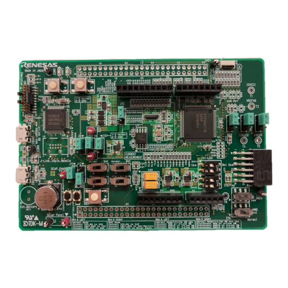
Evaluation Kit RE01 256KB 1.Overview Board Exterior The exterior of Evaluation Kit RE01 256KB is shown in this chapter. Figure 1-1 and Figure 1-2 show the exterior of the main board. Figure 1-3 and Figure 1-4 show the exterior of MIP-LCD expansion board. Figure 1-1: Main Board (Top) Figure 1-2: Main Board (Bottom) R20UT4801EJ0101 Rev.1.01... - Page 12 Evaluation Kit RE01 256KB 1.Overview Figure 1-3: MIP-LCD Expansion Board (Top) Figure 1-4: MIP-LCD Expansion Board (Bottom) R20UT4801EJ0101 Rev.1.01 Page 12 of 77 Oct 02, 2020...
-
Page 13: Board Layout
Evaluation Kit RE01 256KB 2.Board Layout 2. Board Layout Component Layout The component layout of Evaluation Kit are shown in Figure 2-1 and Figure 2-2. Figure 2-1: Main Board Layout MIP-LCD Panel FPC Connector PMOD1 Main Board Interface Figure 2-2: MIP-LCD Expansion Board Layout R20UT4801EJ0101 Rev.1.01 Page 13 of 77 Oct 02, 2020... -
Page 14: Board Dimensions
Evaluation Kit RE01 256KB 2.Board Layout Board Dimensions Figure 2-3 and Figure 2-4 below show the board dimensions and connector positions. All the through-hole connectors are on a common 2.54 mm pitch grid for easy interfacing. Figure 2-3: Main Board Dimensions (Unit: mm) R20UT4801EJ0101 Rev.1.01 Page 14 of 77 Oct 02, 2020... - Page 15 Evaluation Kit RE01 256KB 2.Board Layout Figure 2-4: MIP-LCD Expansion Board Dimension (Unit: mm) R20UT4801EJ0101 Rev.1.01 Page 15 of 77 Oct 02, 2020...
-
Page 16: Component Placement
Evaluation Kit RE01 256KB 2.Board Layout Component Placement Figure 2-5, Figure 2-6, and Figure 2-7 Evaluation Kit show placement of individual components of Component types and values are shown on the board schematics. GND1 GND2 SW1 SW2 P OWER1 J-Link_ 10pin_Needle GND3 SW11... - Page 17 Evaluation Kit RE01 256KB 2.Board Layout R111 R112 R119 R120 R121 R123 R124 R125 R126 R127 R128 R129 R130 R131 R133 R134 R135 R138 Figure 2-6: Main Board Component Placement (Bottom-Side View) R20UT4801EJ0101 Rev.1.01 Page 17 of 77 Oct 02, 2020...
- Page 18 Evaluation Kit RE01 256KB 2.Board Layout PMOD1 Figure 2-7: MIP-LCD Component Placement (Top-Side View) R20UT4801EJ0101 Rev.1.01 Page 18 of 77 Oct 02, 2020...
-
Page 19: Board Initial Settings
Evaluation Kit RE01 256KB 2.Board Layout Board Initial Settings The switch settings of the default kit configuration are as follows. The component layout is shown in Figure 2-8 and the detailed settings are shown in Table 2-1. J15: 1-2 short J7: 1-2 short J9: 1-2 short J5: 1-2 short... -
Page 20: Internal Board Connections
Evaluation Kit RE01 256KB 3.Internal Board Connections 3.Internal Board Connections Figure 3-1 shows the connectivity between Evaluation Kit and RE01. J-Link Energy Harvest Circuit USB Connector Control MCU Solar Panel Interface (Micro-B) (S124) External Battery Interface Supercapacitor Emulator Connector MIP-LCD Expansion Board RESET Control Interface Circuit... -
Page 21: Power Supply
Evaluation Kit RE01 256KB 4.Power Supply 4. Power Supply Power Supply System Figure 4-1 shows power supply system diagram of Evaluation kit. J-Link 5.0V VCC/IOVCC to 3.3V 5.0V to 3.3V Voltage Regulator Voltage Regulator Micro-B Connector Control MCU USB Cable (USB1) RE01-256KB (U6) -
Page 22: Power Supply Source
Evaluation Kit RE01 256KB 4.Power Supply Power Supply Source Evaluation Kit is supplied by emulator through USB cable. The details of power supply components are shown in Figure 4-2 and Table 4-1. When the Evaluation Kit is connected to another system then that system should supply power to the Evaluation Kit. -
Page 23: External Power Supply
Evaluation Kit RE01 256KB 4.Power Supply External Power Supply It is possible to supply voltage to RE01 power terminal by using external power supply. Normally, the emulator supplies voltage equivalent to 3.3V, which is the voltage value after reduction by the regulator. (excluding device which can supply 3.3V) 4.3.1 All power pins... - Page 24 Evaluation Kit RE01 256KB 4.Power Supply 4.3.2 IOVCC0 Figure 4-4 shows the component layout. Follow the steps below when supplying voltage from external power supply to IOVCC0 pin: Open J6 jumper pin 1-2 and 2-3. Supply voltage (1.62V – 3.6V) to any power supply pins other than IOVCC0 pin. Supply voltage to T4.
- Page 25 Evaluation Kit RE01 256KB 4.Power Supply 4.3.3 IOVCC1 Figure 4-5 shows the component layout. Follow the steps below when supplying voltage from external power supply to IOVCC1 pin: Open J7 jumper pin 1-2 and 2-3. Supply voltage (1.62V – 3.6V) to any power supply pins other than IOVCC1 pin. Supply voltage to T1.
- Page 26 Evaluation Kit RE01 256KB 4.Power Supply 4.3.4 AVCC0 The component layout are shown in Figure 4-6 and Figure 4-7. Follow the steps below when supplying voltage from external power supply to AVCC0 pin: Remove R108. Fit R107. Supply voltage (1.62V – 3.6V) to any power supply pins other than AVCC0 pin. Supply voltage to T5.
- Page 27 Evaluation Kit RE01 256KB 4.Power Supply R107: fitted R108: removed Figure 4-7: Component Layout (External Power Supply (Bottom)) R20UT4801EJ0101 Rev.1.01 Page 27 of 77 Oct 02, 2020...
- Page 28 Evaluation Kit RE01 256KB 4.Power Supply 4.3.5 VREFH0 The component layout and settings are shown in Figure 4-8. Follow the steps below when supplying voltage from external power supply to VREF0 pin: Remove R54 and R55 Fit R56. Short J5 jumper pin 1-2. Supply voltage (1.62V –...
-
Page 29: Operation/Start-Up Mode
Evaluation Kit RE01 256KB 5.Operation/Start-up Mode 5. Operation/Start-up Mode Evaluation Kit for RE01 supports 2 operation and start-up modes: normal and energy harvesting (hereinafter, EHC). Normal Operation In normal operation, power is supplied from emulator or external power supply. To use normal operation mode, several switch settings must be made. -
Page 30: Ehc Operation
Evaluation Kit RE01 256KB 5.Operation/Start-up Mode EHC Operation RE01 supports energy harvesting function. In EHC operation, the power is supplied from the included solar panel. User circuit can start operating when voltage is supplied to VSC_VCC pin of RE01. Switch settings are required to operate the energy harvesting function. The related component layout and setting details are shown in Figure 5-2, Table 5-2, and Table 5-3. - Page 31 Evaluation Kit RE01 256KB 5.Operation/Start-up Mode 5.2.1 Solar Panel This product is equipped with solar panel interface (T9, T10). The component layout and details are displayed in Figure 5-3 and Table 5-4. Connect the included solar panel to T9 and T10 using the attached IC clip.
- Page 32 Evaluation Kit RE01 256KB 5.Operation/Start-up Mode 5.2.2 Supercapacitor / External Battery Supercapacitor / external battery can be connected to VBAT_EHC pin in RE01. Switch settings are required in order to use supercapacitor / external battery. Component layout and configuration details are shown in Figure 5-4 and Table 5-5.
- Page 33 Evaluation Kit RE01 256KB 5.Operation/Start-up Mode Make sure that the external battery is already installed before selecting the external battery. The component layout and setting are described in Figure 5-4 and Table 5-7. The recommended external battery is SLB Series (Nichicon). Because the included solar panel* generates 42µA, it might take time to charge the recommended external battery, depending on the operation setting of RE01.
- Page 34 (charged) is used. The program has to be downloaded to RE01 internal flash memory in advance. Sample code is also available on Renesas website, entitled “Maintenance free power management by RE energy harvesting controller (R01AN4837)”.
- Page 35 (charged) is used. The program has to be downloaded to RE01 internal flash memory in advance. Sample code is also available on Renesas website, entitled “Energy harvesting launch operation and quick start SMIP display demo using Evaluation Kit RE01 256KB (R01AN5406)”.
- Page 36 Evaluation Kit RE01 256KB 5.Operation/Start-up Mode 5.2.5.3 When using Parallel MIP-LCD during Secondary Battery Charging Period Follow the steps below to operate parallel MIP LCD during secondary battery charging period. The setting below are intended for the case where supercapacitor (charged) is used. The program has to be downloaded to RE01 internal flash memory in advance.
- Page 37 Evaluation Kit RE01 256KB 5.Operation/Start-up Mode 5.2.5.4 Discharge Switch (SW7, SW8) Discharge switches are included in the main board. SW7 is used to discharge RE01 VCC/IOVCC power supply line. SW8 is used to discharge storage capacitors (C25, C29, and C30). This discharge switches must be used when the user uses energy harvesting function, operate the main board, then restart the energy harvesting function again from the beginning.
-
Page 38: Re01 Start-Up Mode
Evaluation Kit RE01 256KB 5.Operation/Start-up Mode RE01 Start-up Mode RE01 supports 3 start-up modes. Switch settings are necessary to select the start-up mode. Component layout and settings related to start-up modes are explained in Figure 5-10 and Table 5-11. For more details of start-up modes for RE01, refer to RE01 Group User’s Manual’s Hardware. -
Page 39: Debug
Evaluation Kit RE01 256KB 6.Debug 6. Debug This board supports emulators as listed in Table 6-1. Table 6-1: Supported Emulators Supported Emulator Chapter Reference J-Link I-Jet , J-Link 6.3, 6.4 J-Link This main board is equipped with Segger J-Link OB. RE01 debugging is possible by connecting the included USB cable to this board and host PC. - Page 40 Evaluation Kit RE01 256KB 6.Debug 6.1.2 Debugger Connections Figure 6-2 shows the connections between main board (J-Link OB) and host PC. When using J-Link OB, do not connect to other emulators. USB cable Main Board HOST PC Figure 6-2: Debugger Connection Diagram (J-Link R20UT4801EJ0101 Rev.1.01 Page 40 of 77 Oct 02, 2020...
-
Page 41: I-Jet Tm , J-Link Tm
Evaluation Kit RE01 256KB 6.Debug I-jet , J-Link This main board can connect to IAR I-jet emulator or Segger J-Link emulator. RE01 can be debugged by using these emulators. 6.2.1 Component Layout and Settings when using I-jet , J-Link When using the emulator, several switch and resistor settings must be set. Figure 6-3 and Table 6-3 shows the component layout and detailed settings. - Page 42 Evaluation Kit RE01 256KB 6.Debug 6.2.2 Debugger Connections Figure 6-4 shows the connections between main board, emulator, and host PC. When using these emulators (emulators excluding J-Link OB), do not connect the J-Link OB (USB cable). User Interface cable USB cable Emulator Main Board HOST PC...
- Page 43 Evaluation Kit RE01 256KB 6.Debug This main board can connect to Renesas E2 emulator. RE01 can be debugged by using this emulator. 6.3.1 Component Layout and Settings when using E2 When using the emulator, several switch and resistor settings must be set. Figure 6-5 and Table 6-4 shows the component layout and detailed settings.
-
Page 44: Flash Programmer
Evaluation Kit RE01 256KB 6.Debug Flash Programmer This main board supports Renesas Flash Programmer (RFP) for writing programs to RE01’s internal flash memory. Writing can be performed by using E2 emulator and an USB cable. 6.4.1 When using E2 Emulator A program can be written from host PC to RE01’s internal flash memory via E2 emulator. - Page 45 Evaluation Kit RE01 256KB 6.Debug 6.4.2 When using USB Cable (USB Serial) A program can be written from host PC to RE01’s internal flash memory by using USB cable. To use RFP, switch and resistor settings must be set. Component layout and detailed settings are shown in Figure 6-7 and Table 6-6.
- Page 46 Evaluation Kit RE01 256KB 6.Debug 6.4.3 Debugger Connections Figure 6-8 shows the connection between the main board, emulator, and host PC. When using flash programmer, do not connect emulators for purposes other than flash programmer. User Interface cable USB cable E2 Emulator USB cable Main Board...
-
Page 47: Current Measurement Circuit
This main board can measure the current consumption of RE01. shows the current flow that can be measured with the default settings. Sample code is also available on Renesas website, entitled “RE01 256KB Group Low Power Mode Transition Example” (R01AN5337). -
Page 48: Component Layout And Setting During Current Measurement
Evaluation Kit RE01 256KB 7.Current Measurement Circuit Component Layout and Setting during Current Measurement. Switch settings are required to be set before measuring the current. Component layout is shown in Figure 7-2, while details are shown in Figure 7-2 and Table 7-1. When measuring the current consumption, do not connect peripheral circuits such as MIP-LCD. -
Page 49: User Circuitry
Evaluation Kit RE01 256KB 8.User Circuitry 8. User Circuitry Reset Circuit This main board has built-in power-on reset circuit and a reset circuit that is triggered by a switch press. When power is supplied, RE01 is reset by the built-in power-on reset circuit. Pressing RES switch also resets RE01. -
Page 50: Clock Circuit
Evaluation Kit RE01 256KB 8.User Circuitry Clock Circuit The main board has clock circuit to supply clock to RE01. For details on the RE01 clock, refer to RE01 Group User’s Manual Hardware. For details on the main board clock circuit, refer to the main board circuit diagram. Figure 8-2 and Table 8-1 shows the component layout and details. -
Page 51: Switches
Evaluation Kit RE01 256KB 8.User Circuitry Switches This main board has a total of 13 switches. Figure 8-3 and Table 8-2 show the layout and function of each switch. User Switch (SW1) Operation Mode Switch (SW4) User Switch (SW2) Operation Mode Switch (SW3) Start-up Mode Switch (SW9) Internal LDO Switch (SW11) Operation Mode Switch (SW5) -
Page 52: Led
Evaluation Kit RE01 256KB 8.User Circuitry There are 4 LEDs in this main board. Figure 8-4 shows the component layout of the LEDs. Table 8-3 shows the details of the LEDs. LED1 LED0 POWER1 LED2 Figure 8-4: Component Layout (LED) Table 8-3: LED RE01 Color... -
Page 53: Pmod™ Interface
Evaluation Kit RE01 256KB 8.User Circuitry Pmod™ Interface interface. Table 8-4 shows compatible connection boards This main board has the connector for Pmod and Figure 8-5 shows the pin assignment. Table 8-4: Compatible Connection Boards Compatible Boards Reference Chapter MIP-LCD Expansion Board 7.5.1 RL78/G1D BLE Module Expansion Board 7.5.2... - Page 54 This function is supported in default configuration, as supplied. To return to this setting from other settings, set the resistors as shown in Figure 8-6, Figure 8-7, and Table 8-5. Sample code related to this expansion board is available on the Renesas website entitled “R_GDT Driver Sample Code (Using CMSIS Driver Package) ” (R01AN4755).
- Page 55 Evaluation Kit RE01 256KB 8.User Circuitry R121: Fitted R125: Fitted R127: Fitted R129: Fitted R134: Fitted Other settings will be as per the default kit configuration, as supplied. Figure 8-7: Component Layout and Settings (MIP-LCD Expansion Board (Bottom)) Table 8-5: Configuration Details (MIP-LCD Expansion Board) Component Setting R70, R87-R90...
- Page 56 This function is not supported in default configuration, as supplied. Set the resistors as shown in Figure 8-8, Figure 8-9, and Table 8-7. Sample code related to this expansion board is available on the Renesas website entitled “Bluetooth ® Energy Protocol Stack Evaluation Kit RE01 256KB Host Sample” (R01AN5472).
- Page 57 Evaluation Kit RE01 256KB 8.User Circuitry R121: Removed R125: Removed R127: Removed R129: Removed 実装 R134: Removed Other settings will be as per the default kit configuration, as supplied. Figure 8-9: Component Layout and Settings (RL78/G1D BLE Module Expansion Board (Bottom)) Table 8-7: Configuration Details (RL78/G1D BLE Module Expansion Board) Component Setting...
-
Page 58: Usb Serial Conversion
This function is not supported in default configuration, as supplied. To return to this setting from other settings, set the resistors as shown in Figure 8-10 and Table 8-9. The related sample code is available on Renesas Website, entitled “USART Asynchronous Communication Sample Code (Using CMSIS Driver Package) ” (R01AN4699). - Page 59 Evaluation Kit RE01 256KB 8.User Circuitry Prepare the driver provided by FTDI chip before using this function. The necessary driver is listed below. VIRTUAL CON PORT(VCP) Drivers • Please download the driver installer from the following URL. http://www.ftdichip.com/Products/ICs/FT230X.html R20UT4801EJ0101 Rev.1.01 Page 59 of 77 Oct 02, 2020...
-
Page 60: Mlcd (Memory In Pixel Liquid Crystal Display) Interface
Component layout is shown in Figure 8-11, while MIP-LCD connection details is shown in Table 8-11. This function is supported in default configuration, as supplied. Related sample code is available in Renesas Website, entitled “MLCD Transfer Sample Code (Using CMSIS Driver Package) ” (R01AN4883). -
Page 61: Flash Memory
Evaluation Kit RE01 256KB 8.User Circuitry Flash Memory This main board has a 64Mb flash memory made by Macronix (MX25R6435FM2IL0). Connection to the flash memory is done through RE01 built-in quad serial peripheral interface (QSPI). Component layout is shown in Figure 8-12, while the details of flash memory connection is shown in Table 8-13. -
Page 62: Arduino Uno Interface
Evaluation Kit RE01 256KB 8.User Circuitry Arduino UNO Interface This main board has Arduino UNO interface and can be connected to various shields. Component layout and configuration details are shown in Figure 8-13, Figure 8-14, and Table 8-14. Details of Arduino UNO connections are shown in Table 8-15, Table 8-16, Table 8-17, and Table 8-18. - Page 63 Evaluation Kit RE01 256KB 8.User Circuitry R109: Removed R110: Removed Other settings will be as per the default kit configuration, as supplied. Figure 8-14: Component Layout and Settings (Arduino UNO Interface (Bottom)) Table 8-14: Configuration Details (Arduino UNO Interface) Component Setting Fitted R109, R110...
- Page 64 Evaluation Kit RE01 256KB 8.User Circuitry Table 8-16: Arduino UNO Interface (2) Arduino UNO Interface (J4) RE01 RE01 Signal Name Signal Name Port Port P314 P602 ARDUINO_IO0_RXD5_B ARDUINO_IO4 (IOVCC1) (IOVCC1) P315 P603 ARDUINO_IO5_ ARDUINO_IO1_TXD5_B GTIOC5A_B (IOVCC1) (IOVCC1) P204 P604 ARDUINO_IO6_ ARDUINO_IO2_IRQ7_B GTIOC5B_B (IOVCC1)
-
Page 65: External Dc/Dc Circuit
Component layout is shown in Figure 8-15, while details are shown in Figure 8-15 and Table 8-19. Sample code is also available on Renesas website, entitled “RE01 256KB Group How to reduce power consumption by using the external DC/DC converter” (R01AN5424). -
Page 66: Headers
Evaluation Kit RE01 256KB 9.Headers 9. Headers RE01 Headers This main board has RE01 headers, which can be used to observe general I/O port. Table 9-1 and Table 9-2 shows the connections of RE01 header J1. Table 9-3 and Table 9-4 shows the connections of RE01 header Table 9-1: RE01 Header J1 Connections (1) RE01 Header J1 Function (General IO... - Page 67 Evaluation Kit RE01 256KB 9.Headers Table 9-2: RE01 Header J1(2) RE01 Header J1 Function (General IO Function (General IO Port/Power) Port/Power) RE01 Pin RE01 Pin Circuit Net Name Circuit Net Name P200 J1_P200 GROUND VCC_SU VBAT_EHC VCC_SU VBAT_EHC VSC_VCC VSC_VCC GROUND Reserve P210...
- Page 68 Evaluation Kit RE01 256KB 9.Headers Table 9-3: RE01 Header J2(1) RE01 Header J2 Function (General IO Function (General IO Port/Power) Port/Power) RE01 Pin RE01 Pin Circuit Net Name Circuit Net Name P604 P603 ARDUINO_IO6_GTIOC5B_B ARDUINO_IO5_GTIOC5A_B P602 P601 ARDUINO_IO4 J2_P601 P600 P113 J2_P600 MLCD_VCOM...
- Page 69 Evaluation Kit RE01 256KB 9.Headers Table 9-4: RE01 Header J2(2) RE01 Header J2 Function (General IO Function (General IO Port/Power) Port/Power) RE01 Pin RE01 Pin Circuit Net Name Circuit Net Name P508 P501 J2_P501 P500 AVCC0 J2_P500 AVCC0 P007 GROUND J2_P007 P006 P005...
-
Page 70: Code Development
OB that is mounted on Main Board. • Connect Main Board to PC through Segger development tool J-Link emulator. • Connect Main Board to PC through Renesas development tool E2 emulator. • Refer to the manufacturer’s website for more details about each emulator. 10.2 Mode Support This Evaluation Kit supports several operation modes and start-up modes. -
Page 71: Additional Information
Copyright This document may be, wholly or partially, subject to change without notice. All rights reserved. Duplication of this document, either in whole or part is prohibited without the written permission of Renesas Electronics Corporation. © 2020 Renesas Electronics Corporation. All rights reserved. - Page 72 RE01Group Revision History Evaluation Kit RE01 256KB User’s Manual Rev. Date Description Page Summary 1.00 Jul 07, 2020 First Edition issued. - 1.01 Oct 02, 2020 Add chapter 1.2 Kit Contents. Change table 1-2. Add figure 2-8. Change figure 4-1. Add chapter 4.3.1 All power pins.
- Page 73 RE01 Group Evaluation Kit RE01 256KB User’s Manual Publication Date: Rev. 1.01 Oct 02, 2020 Published by: Renesas Electronics Corporation...
- Page 74 SALES OFFICES Refer to "http://www.renesas.com/" for the latest and detailed information. Renesas Electronics Corporation TOYOSU FORESIA, 3-2-24 Toyosu, Koto-ku, Tokyo 135-0061, Japan Renesas Electronics America Inc. Milpitas Campus 1001 Murphy Ranch Road, Milpitas, CA 95035, U.S.A. Tel: +1-408-432-8888, Fax: +1-408-434-5351 Renesas Electronics America Inc.
- Page 75 RE01 Group R20UT4801EJ0101...
- Page 76 Mouser Electronics Authorized Distributor Click to View Pricing, Inventory, Delivery & Lifecycle Information: Renesas Electronics RTK70E0118S00000BJ...
Need help?
Do you have a question about the RE0 Series and is the answer not in the manual?
Questions and answers