Table of Contents
Advertisement
Quick Links
RE01 Group
32
32
RE Family / RE0 Series
All information contained in these materials, including products and product specifications, represents
information on the product at the time of publication and is subject to change by Renesas Electronics
Corporation without notice. Please review the latest information published by Renesas Electronics
Corporation through various means, including the Renesas Electronics Corporation website
(http://www.renesas.com).
Evaluation Kit RE01 1500KB User's Manual
Rev. 2.00 Aug 2020
Advertisement
Table of Contents

Related Manuals for Renesas RE01 Series


Summary of Contents for Renesas RE01 Series
- Page 1 All information contained in these materials, including products and product specifications, represents information on the product at the time of publication and is subject to change by Renesas Electronics Corporation without notice. Please review the latest information published by Renesas Electronics Corporation through various means, including the Renesas Electronics Corporation website (http://www.renesas.com).
- Page 2 Renesas Electronics disclaims any and all liability for any damages or losses incurred by you or any third parties arising from the use of any Renesas Electronics product that is inconsistent with any Renesas Electronics data sheet, user’s manual or other Renesas Electronics document.
- Page 3 Products The following usage notes are applicable to all Microprocessing unit and Microcontroller unit products from Renesas. For detailed usage notes on the products covered by this document, refer to the relevant sections of the document as well as any technical updates that have been issued for the products.
- Page 4 Evaluation Kit, even if Renesas or its affiliates have been advised of the possibility of such damages.
- Page 5 The following documents apply to Evaluation Kit for RE01 1500KB. Make sure to refer to the latest versions of these documents. The newest versions of the documents listed may be obtained from the Renesas Electronics Web site.
- Page 6 Dual In-line Package Direct Memory Access DMAC Direct Memory Access Controller Do Not Fit Renesas On-chip Debugging Emulator studio Renesas Eclipse-based Integrated Development Environment EEPROM Electronically Erasable Programmable Read Only Memory Energy Harvesting Energy Harvesting Control Circuit Electromagnetic Compatibility Electrostatic Discharge...
-
Page 7: Table Of Contents
Table of Contents 1. Overview ..........................8 Purpose ..............................8 Board specification ............................. 9 Board Exterior ............................10 2. Board Layout ........................12 Board Function ............................12 Board Dimensions ............................ 15 Component Placement ..........................17 3. Internal Board Connections ..................... 20 4. -
Page 8: Overview
Evaluation Kit RE01 1500KB R20UT4379EJ0200 Rev.2.00 Aug 04, 2020 1. Overview Purpose This Evaluation Kit is an evaluation tool for Renesas RE01 device. This manual describes the technical details of the Evaluation Kit hardware. R20UT4379EJ0200 Rev.2.00 Page 8 of 77 Aug 04, 2020... -
Page 9: Board Specification
Evaluation Kit RE01 1500KB 1. Overview Board specification Board specification was shown in Table 1-1, Table 1-2. Table 1-1: Board Specification Item Specification Part No : R7F0E015D2CFB Target Device Package : 144-pin LFQFP On-Chip Memory : ROM 1.5MB, RAM 256KB On-Board Memory SPI Serial Flash: 64Mbit RE01 Main: 32MHz... -
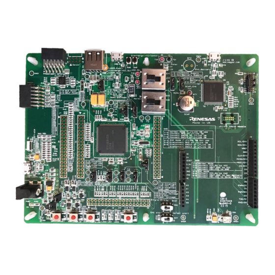
Page 10: Board Exterior
Evaluation Kit RE01 1500KB 1. Overview Board Exterior Figure 1-1 show the exterior of main board. Figure 1-2 show the exterior of MIP-LCD Expansion board. Bottom Figure 1-1: Main Board External View R20UT4379EJ0200 Rev.2.00 Page 10 of 77 Aug 04, 2020... - Page 11 Evaluation Kit RE01 1500KB 1. Overview Bottom Figure 1-2: MIP-LCD Expansion Board External View R20UT4379EJ0200 Rev.2.00 Page 11 of 77 Aug 04, 2020...
-
Page 12: Board Layout
Evaluation Kit RE01 1500KB 2. Board Layout 2. Board Layout Board Function Figure 2-1 and Figure 2-2 show the functions of the Evaluation Kit Board.Table 2-1, Table 2-2 and Table 2-3 show their setting details. External battery PMOD2 (QSPI) interface Solar panel interface J-Link OB Debugger... - Page 13 Evaluation Kit RE01 1500KB 2. Board Layout Figure 2-2: Board Function2 R20UT4379EJ0200 Rev.2.00 Page 13 of 77 Aug 04, 2020...
- Page 14 Evaluation Kit RE01 1500KB 2. Board Layout Table 2-3: Jumper Function Item Function Setting ( * is initial setting ) 1-2 short: USE BT2 Battery Battery Select(VBAT) 2-3 short: USE Super Capacitor * USBFS Host/Function Select 1-2 short: Host Mode 2-3 short: Function Mode * Self/Bus-powered Configuration 1-2 short: Bus-powered...
-
Page 15: Board Dimensions
Evaluation Kit RE01 1500KB 2. Board Layout Board Dimensions Figure 2-3, Figure 2-4 show the board dimensions and connector positions. All the through-hole connectors are on a common 2.54mm pitch grid for easy interfacing. USB_2 PMOD2 USB_1 Sensor SCAP Func 5.9mm 54.16mm 70.94mm... - Page 16 Evaluation Kit RE01 1500KB 2. Board Layout MIP-LCD Panel PMOD1 55.0mm 4.0mm phai 12.0mm phai Figure 2-4: MIP-LCD Expansion Board Dimensions R20UT4379EJ0200 Rev.2.00 Page 16 of 77 Aug 04, 2020...
-
Page 17: Component Placement
Evaluation Kit RE01 1500KB 2. Board Layout Component Placement Figure 2-5, Figure 2-6, Figure 2-7 show placement of individual components of Evaluation Kit. Component types and values are shown on the board schematics. PMOD2 USB_2 USB1 Sensor1 USB_1 GND2 D1 D2 GND1 D5 D6 R294... - Page 18 Evaluation Kit RE01 1500KB 2. Board Layout R183 R185 R186 R187 R188 R184 R189 R191 R192 R194 R195 R198 R199 R202 R203 R293 R205 R206 R208 R209 R211 R212 R213 R190 R214 R215 R216 R193 R217 R197 R218 R219 R290 R289 R235 R292...
- Page 19 Evaluation Kit RE01 1500KB 2. Board Layout PMOD1 Figure 2-7: MIP-LCD Expansion Board Component Placement (Top) R20UT4379EJ0200 Rev.2.00 Page 19 of 77 Aug 04, 2020...
-
Page 20: Internal Board Connections
Evaluation Kit RE01 1500KB 3. Internal Board Connections 3. Internal Board Connections Figure 3-1 shows the Evaluation Kit components and their connectivity to RE01. 5V DC PWR IN (5V) ・AC Adapter ・USB VBUS ・J-Link OB debugger ・I-jet debugger Pow er LED DCDC Converter DCDC Converter Jumper... -
Page 21: Power Source
Evaluation Kit RE01 1500KB 4. Power Source 4. Power Source Power System Figure 4-1 shows the power supply diagram of the Evaluation Kit. J-Link 5.0V 5.0V to 3.3V Voltage Regulator Micro-B Connector VCC/IOVCC to 3.3V Control MCU USB Cable Load Switch (USB1) Voltage Regulator (U7) -
Page 22: Power Supply
Evaluation Kit RE01 1500KB 4. Power Source Power Supply The Evaluation Kit can draw power from the emulator, USB cable, or DC Power Jack. Details are shown in Figure 4-2 and Table 4-1 . If the Evaluation Kit is connected to another system, supply power to the Evaluation Kit from that system. -
Page 23: External User Voltage Supply
Evaluation Kit RE01 1500KB 4. Power Source External User Voltage Supply External user voltage supply between 1.62V – 3.6V can be applied to RE01. Details are shown in Figure 4-3 and Table 4-2. J22 open and connect a stabilized power supply to pin 2 of J22. A convenient ground is available near J22 [GND6]. -
Page 24: Debug
Evaluation Kit RE01 1500KB 5. Debug 5. Debug J-Link™ OB This main board is equipped with Segger J-Link™ OB. RE01 debugging is possible by connecting the bundled USB cable to this board and host PC. 5.1.1 Component Layout and Settings Figure 5-1 shows the component layout. - Page 25 Evaluation Kit RE01 1500KB 5. Debug 5.1.2 Debugger Connection Figure 5-2 shows the connections between main board (J-Link™ OB) and host PC. When using J-Link™ OB, do not connect to other emulators. USB1 connect Figure 5-2: Debugger Connection Diagram R20UT4379EJ0200 Rev.2.00 Page 25 of 77 Aug 04, 2020...
-
Page 26: I-Jet/J-Link
Evaluation Kit RE01 1500KB 5. Debug I-jet/J-Link™ This main board can connect to an IAR I-jet or Segger J-Link™ emulator. RE01 debugging is possible by using either of these emulators 5.2.1 Component Layout and Settings Figure 5-3 shows the component layout. To use the emulator, switch settings are required. For details, see the settings in Figure 5-3 and Table 5-2. - Page 27 Evaluation Kit RE01 1500KB 5. Debug 5.2.2 Debugger Connection Figure 5-4 shows the connections between main board, emulator and host PC. When using the I-jet/J-Link™ emulator, do not use other emulators. CN2 connect Figure 5-4: Debugger Connection Diagram R20UT4379EJ0200 Rev.2.00 Page 27 of 77 Aug 04, 2020...
-
Page 28: E2 Emulator
Evaluation Kit RE01 1500KB 5. Debug E2 Emulator This main board can connect to a Renesas E2 emulator, RE01 debugging is possible by using this emulator. 5.3.1 Component Layout and Settings Figure 5-5 shows the component layout. To use the emulator, several settings to switches and resistors must be made. - Page 29 Evaluation Kit RE01 1500KB 5. Debug 5.3.2 Debugger Connection Figure 5-6 shows the connections between main board, emulator and host PC. When using E2 emulator, do not use other emulators. CN2 connect Figure 5-6: Debugger Connection Diagram R20UT4379EJ0200 Rev.2.00 Page 29 of 77 Aug 04, 2020...
-
Page 30: Flash Programmer
Evaluation Kit RE01 1500KB 5. Debug Flash Programmer This main board supports a Renesas Flash Programmer (RFP) for writing programs to RE01’s built-in flash memory. Writing can be performed by using E2 emulator or USB cable. 5.4.1 When using E2 Emulator A program can be written from the host PC to RE01’s built-in flash memory via an E2 emulator. - Page 31 Evaluation Kit RE01 1500KB 5. Debug 5.4.1.2 How To Use Follow the procedures below. 1. Set the switches and resistors on the main board as shown in Table 5-4. 2. Connect the emulator connector (CN2) to the host PC via E2 emulator. 3.
- Page 32 Evaluation Kit RE01 1500KB 5. Debug 5.4.2 When using the USB Cable (USB serial) A program can be written from the host PC to RE01’s built-in flash memory using a USB cable. 5.4.2.1 Component Layout and Settings Figure 5-9 and Figure 5-10 shows the component layout. To use RFP, several settings to switches and resistors must be made.
- Page 33 Evaluation Kit RE01 1500KB 5. Debug R183 R185 R186 R187 R188 R184 R189 R191 R192 R194 R195 R198 R199 R202 R203 R293 R205 R206 R208 R209 R211 R212 R213 R190 R214 R215 R216 R193 R217 R197 R218 R290 R219 R190: DNF R289 R292 R235...
- Page 34 Evaluation Kit RE01 1500KB 5. Debug 5.4.2.2 How to Use Follow the procedures below. 1. Set the switches and resistors on the main board as shown in Table 5-5. 2. Connect the USB serial connector (USB2) to host PC via USB cable. 3.
-
Page 35: Operation / Startup Mode Setting
Evaluation Kit RE01 1500KB 6. Operation / Startup mode setting 6. Operation / Startup mode setting Normal Operation The normal operation of this main board is for power to be supplied from an emulator or external PSU. Figure 6-1 shows the component layout. For normal operation, the settings in Table 6-1 must be made. J-Link™... -
Page 36: Ehc Operation
Evaluation Kit RE01 1500KB 6. Operation / Startup mode setting EHC Operation RE01 incorporates an Energy Harvest Circuit (EHC), which can operate even with the weak power from the power generating element. On this main board, some peripheral circuits can be powered by supplying voltage to VSC_VCC pin of RE01 from the solar panel. - Page 37 Evaluation Kit RE01 1500KB 6. Operation / Startup mode setting 6.2.2 EHC Power Supply 6.2.2.1 Power Generating Element This Kit includes a solar panel. To use, it must be connected to the solar panel interface, via T20 and T21. See Figure 6-3.
- Page 38 Evaluation Kit RE01 1500KB 6. Operation / Startup mode setting 6.2.2.2 Supercapacitor / External Battery Either a supercapacitor or an external battery can be connected to VBAT_EHC pin of the RE01. Switches required setting in order to use a supercapacitor or external battery. Figure 6-4 shows the component layout, and Table 6-3 shows details of setting.
- Page 39 Evaluation Kit RE01 1500KB 6. Operation / Startup mode setting 6.2.2.3 Storage Capacitor This main board has a 100uF power storage capacitor connected to VCC_SU pin of RE01. Depending on your design requirements, it may be necessary to alter the capacitance connected to VCC_SU pin. If necessary, mount a capacitor on the C7 footprint (size: 1608).
-
Page 40: Current Measurement Circuit
Evaluation Kit RE01 1500KB 7. Current Measurement Circuit 7. Current Measurement Circuit This main board can measure the current consumption of RE01. Measurement is possible by connecting the ampere meter in series to J20. Figure 7-1 shows the component layout, and Table 7-1 shows details of setting. SW6: EHC Mode J23: Open R158: DNF... -
Page 41: Peripheral Circuits
Evaluation Kit RE01 1500KB 8. Peripheral Circuits 8. Peripheral Circuits Available Peripheral Circuits in each Operation Mode Table 8-1 shows the peripheral circuits that can be used in each operation mode. Table 8-1: Peripheral Circuits that can be used in each Operation Mode Item Normal startup EHC startup... -
Page 42: Reset Circuit
Evaluation Kit RE01 1500KB 8. Peripheral Circuits Reset Circuit This main board has a RE01 built-in power-on reset circuit and a reset circuit triggered by pressing a switch. When power is supplied, RE01 is reset by the built-in power-on reset circuit. Pressing RES switch also resets RE01. -
Page 43: Clock Circuit
Evaluation Kit RE01 1500KB 8. Peripheral Circuits Clock Circuit This main board has clock circuits for clock source of RE01 and clock source of RX621. Refer to “RE01 Group User’s Manual: Hardware” and “RX621 Group Hardware Manual” for details regarding the clock specifications, and “Evaluation Kit Main Board schematics”... -
Page 44: Switches
Evaluation Kit RE01 1500KB 8. Peripheral Circuits Switches This main board has 10 switches. Figure 8-3 and Figure 8-4 shows the component layout, and Table 8-3 shows the function of each switch and their connections. Discharge Switch (SW9) Discharge Switch (SW8) Operation Mode Switch (SW5) Operation Mode Switch (SW6) Mode Switch (SW4) - Page 45 Evaluation Kit RE01 1500KB 8. Peripheral Circuits Mode Switch (Default SW10: L) R183 R185 R186 R187 R188 R184 R189 R191 R192 R194 R195 R198 R199 R202 R203 R293 R205 R206 R208 R209 R211 R212 R213 R190 R214 R215 R216 R193 R217 R197 R218...
-
Page 46: Leds
Evaluation Kit RE01 1500KB 8. Peripheral Circuits LEDs This main board has 4 LEDs. Figure 8-5 shows the component layout, and Table 8-4 shows each luminary color of LEDs and their connections. LED0 LED2 5VPWR LED1 Figure 8-5: Component Layout Table 8-4: LEDs and Connections RE01 Color... -
Page 47: Potentiometer
Evaluation Kit RE01 1500KB 8. Peripheral Circuits Potentiometer A single-turn potentiometer is connected to AN028 (Port P506, Pin 109) of RE01, to provide a variable analog voltage, between GROUND potential and the Board_3V3. Refer to the manufacturer's website for specification of the potentiometer (Maker: Bourns, Inc. - Part Number: 3314 series). -
Page 48: Pmod
Evaluation Kit RE01 1500KB 8. Peripheral Circuits Pmod™ 8.7.1 Pmod™ This main board has connectors for Digilent Pmod™ interface. To PMOD1 and PMOD2, compatible PMOD module must be connected. Also, the bundled MIP-LCD Expansion board can be connected to PMOD1. Figure 8-7 shows the component layout. - Page 49 Evaluation Kit RE01 1500KB 8. Peripheral Circuits The Digilent Pmod™ use an SPI interface. Table 8-5 shows PMOD1’s connections, and Table 8-6 shows PMOD2’s connections. Please note that the connector numbering adheres to the Digilent Pmod™ standard and is different from other connectors pin designs.
- Page 50 Evaluation Kit RE01 1500KB 8. Peripheral Circuits 8.7.2 MIP-LCD Expansion Board Interface The MIP-LCD Expansion board, supplied with this kit, should be connected to the PMOD1 interface, on the main board. PMOD1 is also used for PMOD module connection. MIP-LCD (KYOCERA with part number TN0181ANVNANN-AN00 ) loaded on MIP-LCD Expansion board uses RE01’s built-in Serial Peripheral Interface (SPI).
-
Page 51: Usb Serial Conversion
Evaluation Kit RE01 1500KB 8. Peripheral Circuits USB Serial Conversion SCI4 port of the RE01's built-in serial communication interface (SCI) has been connected to USB serial converter (FT230XQ (FTDI chip)) in the default kit configuration. The USB port will now expose a virtual COM port. - Page 52 Evaluation Kit RE01 1500KB 8. Peripheral Circuits R183 R185 R186 R187 R188 R184 R189 R191 R192 R194 R195 R193: DNF R198 R199 R202 R203 R293 R205 R206 R208 R209 R211 R212 R213 R190 R214 R215 R216 R193 R217 R197 R218 R290 R219 R289...
-
Page 53: Mlcd (Memory In Pixel Liquid Crystal Display) Interface
Evaluation Kit RE01 1500KB 8. Peripheral Circuits MLCD (Memory in Pixel Liquid Crystal Display) Interface 8.9.1 MLCD Function RE01 has 1 channel of MIP Liquid Crystal Controller (MLCD) as built-in, and can be connected to Parallel MIP-LCD (Maker: KYOCERA, Part number: TN0104ANVAANN-GN00*1) through FPC connector (CN3) on the main board. - Page 54 Evaluation Kit RE01 1500KB 8. Peripheral Circuits R183 R185 R186 R187 R188 R184 R189 R191 R192 R194 R195 R198 R199 R202 R203 R293 R205 R206 R208 R209 R211 R212 R213 R190 R214 R215 R216 R193 R217 R197 R218 R290 R219 R289 R235 R292...
- Page 55 Evaluation Kit RE01 1500KB 8. Peripheral Circuits Table 8-10: MLCD Connections RE01 Signal name Function Port MLCD_VCOM Common electrode polarity signal pin P113 MLCD_XRST LCD control output pin P112 MLCD_SCLK Serial output clock pin for communications P111 MLCD_DEN Data identification signal pin P110 MLCD_ENBS Horizontal data enable pin...
-
Page 56: Flash Memory (Qspi)
Evaluation Kit RE01 1500KB 8. Peripheral Circuits 8.10 Flash Memory (QSPI) The main board is supplied with flash memory. Fitted is a 64MB Flash Memory manufactured by Macronix (MX25R6435FM2IL0). The flash memory is connected to RE01’s built-in Quad Serial Peripheral Interface modules (QSPI). Figure 8-15, Figure 8-16 shows the component layout, and Table 8-11 shows Flash Memory connections. - Page 57 Evaluation Kit RE01 1500KB 8. Peripheral Circuits R183 R185 R186 R187 R188 R184 R189 R191 R192 R194 R195 R217: Fit R198 R199 R202 R203 R293 R205 R206 R208 R209 R211 R212 R213 R190 R214 R215 R216 R193 R217 R197 R218 R290 R219 R289...
-
Page 58: Universal Serial Bus (Usb)
Evaluation Kit RE01 1500KB 8. Peripheral Circuits 8.11 Universal Serial Bus (USB) This main board has USB connectors (Type-A, Micro-B). RE01 built-in USB can operate as either a Host or Function device. Table 8-13 shows USB connections. Table 8-13: USB Module Connections RE01 USB Signal name Function... - Page 59 Evaluation Kit RE01 1500KB 8. Peripheral Circuits R183 R185 R186 R187 R188 R184 R189 R191 R192 R194 R195 R198 R199 R202 R203 R293 R205 R206 R208 R209 R211 R212 R213 R190 R214 R215 R216 R193 R217 R197 R218 R290 R219 R289 R292 R235...
- Page 60 Evaluation Kit RE01 1500KB 8. Peripheral Circuits 8.11.2 Function Controller Mode (Self Power) Figure 8-19 shows the component layout. To enable this functionality, several optional resistors must be in place and switch settings made. For details, see the settings in Figure 8-19 and Table 8-15. The default kit configuration, as supplied, will have these resistors in place and switches set as required.
- Page 61 Evaluation Kit RE01 1500KB 8. Peripheral Circuits 8.11.3 Function Controller Mode (Bus Power) By mounting Jumper J3, it is possible to use as bus-powered device. Figure 8-20 shows the component layout. To enable this functionality, several optional resistors must be in place and switch settings made. For details, see the settings in Figure 8-20 and Table 8-16.
-
Page 62: Arduino Uno Interface
Evaluation Kit RE01 1500KB 8. Peripheral Circuits 8.12 Arduino UNO Interface This main board provides an Arduino UNO interface connector, to allow connection to 'Shields'. Figure 8-21 and Figure 8-22 shows the component layout, Table 8-17 shows details of settings, and Table 8-18, Table 8-19, Table 8-20 and Table 8-21 shows Arduino UNO interface connections. - Page 63 Evaluation Kit RE01 1500KB 8. Peripheral Circuits R183 R185 R186 R187 R188 R184 R189 R191 R192 R194 R195 R198 R199 R202 R203 R293 R205 R206 R208 R209 R211 R212 R213 R190 R214 R215 R216 R193 R217 R197 R218 R290 R219 R289 R292 R235...
- Page 64 Evaluation Kit RE01 1500KB 8. Peripheral Circuits Table 8-18: Arduino UNO Interface Connections (1) Arduino UNO Interface Connector (J6) RE01 RE01 Signal name Signal name Port Port ARDUINO-IO6 ARDUINO-RSPCKA_B P011 P702 GROUND ARDUINO-IO7 P202 VREFH0 ARDUINO-SSLA0_B P012 ARDUINO-SDA1 ARDUINO-MOSIA_B P010 P700 ARDUINO-SCL1 ARDUINO-MISOA_B...
-
Page 65: Sensor Board Interface
Evaluation Kit RE01 1500KB 8. Peripheral Circuits 8.13 Sensor Board Interface This main board has through-hole patterns that can be connected to the conventional sensor board with I2C interface. Figure 8-23 and Figure 8-24 shows the component layout, and Table 8-23 shows connections of sensor board interface. - Page 66 Evaluation Kit RE01 1500KB 8. Peripheral Circuits R183 R185 R203: DNF R186 R187 R188 R206: Fit R184 R189 R191 R192 R194 R195 R198 R199 R202 R203 R293 R205 R206 R208 R209 R211 R212 R213 R190 R214 R215 R216 R193 R217 R197 R218 R290...
-
Page 67: External Dcdc Circuit
Evaluation Kit RE01 1500KB 8. Peripheral Circuits 8.14 External DCDC Circuit Normally, the internal power supply of RE01 uses a built-in regulator (LDO). However, RE01 can enable an even lower power consumption by supplying power to the internal power supply from an external DCDC converter instead of the internal LDO. -
Page 68: Headers
Evaluation Kit RE01 1500KB 9. Headers 9.Headers RE01 Headers This main board has RE01 headers, which can be used to observe general purpose ports of RE01. Table 9-1 shows connections of RE01 header J9, Table 9-2 shows connections of RE01 header J7, Table 9-3 shows connections of RE01 header J8, and Table 9-4 shows connections of the RE01 header J21. - Page 69 Evaluation Kit RE01 1500KB 9. Headers Table 9-2: RE01 Header J7 Connections RE01 Header J7 Function (General IO Function (General IO port/Power) port/Power) RE01 Pin RE01 Pin Circuit Net Name Circuit Net Name P610 P609 J7-P610 J7-P609 P608 P607 J7-P608 J7-P607 P606 P605...
- Page 70 Evaluation Kit RE01 1500KB 9. Headers Table 9-3: RE01 Header J8 Connections RE01 Header J8 Function (General IO Function (General IO port/Power) port/Power) RE01 Pin RE01 Pin Circuit Net Name Circuit Net Name 3.3V 5.0V Board_3V3 Board_5V P204 P203 J8-P204 J8-P203 P202 P704...
- Page 71 Evaluation Kit RE01 1500KB 9. Headers Table 9-4: RE01 Header J21 Connections RE01 Header J21 Function (General IO Function (General IO port/Power) port/Power) RE01 Pin RE01 Pin Circuit Net Name Circuit Net Name 3.3V 5.0V Board_3V3 Board_5V P506 P505 J21-P506 J21-P505 P504 P503...
-
Page 72: Code Development
Connect Main Board to PC through Segger development tool J-Link emulator Connect Main Board to PC through Renesas development tool E2 emulator and E2 emulator Lite. Refer to the manufacturer's website for more details about each emulator. -
Page 73: Additional Information
Copyright This document may be, wholly or partially, subject to change without notice. All rights reserved. Duplication of this document, either in whole or part is prohibited without the written permission of Renesas Electronics Corporation. © 2018 - 2020 Renesas Electronics Corporation. All rights reserved. - Page 74 RE01 Group REVISION HISTORY Evaluation Kit RE01 1500KB User’s Manual Description Rev. Date Page Summary 1.00 Jun 26, 2019 First Edition issued. 2.00 Aug 04, 2020 Renewal of configuration C - 1...
- Page 75 RE01 Group Evaluation Kit RE01 1500KB User’s Manual Publication Date: Rev.2.00 Aug 04, 2020 Published by: Renesas Electronics Corporation...
- Page 76 SALES OFFICES Refer to "http://www.renesas.com/" for the latest and detailed information. Renesas Electronics Corporation TOYOSU FORESIA, 3-2-24 Toyosu, Koto-ku, Tokyo 135-0061, Japan Renesas Electronics America Inc. Milpitas Campus 1001 Murphy Ranch Road, Milpitas, CA 95035, U.S.A. Tel: +1-408-432-8888, Fax: +1-408-434-5351 Renesas Electronics America Inc.
- Page 77 RE01 Group R20UT4379EJ0200...
Need help?
Do you have a question about the RE01 Series and is the answer not in the manual?
Questions and answers