Table of Contents
Advertisement
Quick Links
RE01 Group
32
32
RE Family / RE0 Series
All information contained in these materials, including products and product specifications, represents
information on the product at the time of publication and is subject to change by Renesas Electronics
Corporation without notice. Please review the latest information published by Renesas Electronics
Corporation through various means, including the Renesas Electronics Corporation website
(http://www.renesas.com).
Evaluation Kit RE01 1500KB User's Manual
Rev. 1.00 Jun 2019
Advertisement
Table of Contents

Related Manuals for Renesas RE Series


Summary of Contents for Renesas RE Series
- Page 1 All information contained in these materials, including products and product specifications, represents information on the product at the time of publication and is subject to change by Renesas Electronics Corporation without notice. Please review the latest information published by Renesas Electronics Corporation through various means, including the Renesas Electronics Corporation website (http://www.renesas.com).
- Page 2 Renesas Electronics disclaims any and all liability for any damages or losses incurred by you or any third parties arising from the use of any Renesas Electronics product that is inconsistent with any Renesas Electronics data sheet, user’s manual or other Renesas Electronics document.
- Page 3 Products The following usage notes are applicable to all Microprocessing unit and Microcontroller unit products from Renesas. For detailed usage notes on the products covered by this document, refer to the relevant sections of the document as well as any technical updates that have been issued for the products.
- Page 4 Evaluation Kit, even if Renesas or its affiliates have been advised of the possibility of such damages.
- Page 5 The following documents apply to Evaluation Kit for RE01 1500KB. Make sure to refer to the latest versions of these documents. The newest versions of the documents listed may be obtained from the Renesas Electronics Web site.
- Page 6 Cyclic Redundancy Check Digital-to-Analog Converter Dual In-line Package Direct Memory Access DMAC Direct Memory Access Controller Do Not Fit Renesas On-chip Debugging Emulator EEPROM Electronically Erasable Programmable Read Only Memory Energy Harvesting Energy Harvesting Control Circuit Electromagnetic Compatibility Electrostatic Discharge...
-
Page 7: Table Of Contents
Table of Contents 1. Overview ..........................9 Purpose ..............................9 Board specification ........................... 10 2. Power Supply ........................12 Requirements ............................12 3. Board Layout ........................13 Component Layout ........................... 13 Board Dimensions ............................ 14 Component Placement ..........................16 4. Connectivity ........................19 Internal Board Connections ........................ - Page 8 8. Code Development ......................53 Overview ..............................53 Mode Support ............................53 Address Space ............................53 9. Additional Information ...................... 54...
-
Page 9: Overview
Rev. 1.00 Jun 26, 2019 1. Overview Purpose This Evaluation Kit is an evaluation tool for Renesas RE01 device. This manual describes the technical details of the Evaluation Kit hardware. R20UT4379EJ0100 Rev. 1.00 Page 9 of 58 Jun 26, 2019... -
Page 10: Board Specification
Evaluation Kit RE01 1500KB 1. Overview Board specification Board specification was shown in Table 1-1,Table 1-2 below. Table 1-1: Board Specification Item Specification Part No : R7F0E015D2CFB Target Device Package : 144-pin LFQFP On-Chip Memory : ROM 1.5MB, RAM 256KB On-Board Memory SPI Serial Flash: 64Mbit RE01 Main: 32MHz... - Page 11 Evaluation Kit RE01 1500KB 1. Overview Table 1-2: MIP-LCD Expansion Board Specification Item Specification Part No: TN0181ANVNANN-AN00 (KYOCERA) MIP-LCD Size: 1.81 inch Resolution: 200dpi (256(H) x 256(V)) Main Board Interface 2.54mm pitch: 12-pin x 1(PMOD1) : Please contact KYOCERA. R20UT4379EJ0100 Rev. 1.00 Page 11 of 58 Jun 26, 2019...
-
Page 12: Power Supply
Evaluation Kit RE01 1500KB 2. Power Supply 2. Power Supply Requirements This Evaluation Kit was supplied with power supply from emulator. The detail was shown in Table 2-1. When the Evaluation Kit is connected to another system then that system should supply power to the Evaluation Kit. This board has an optional center positive supply connector using a barrel power jack. -
Page 13: Board Layout
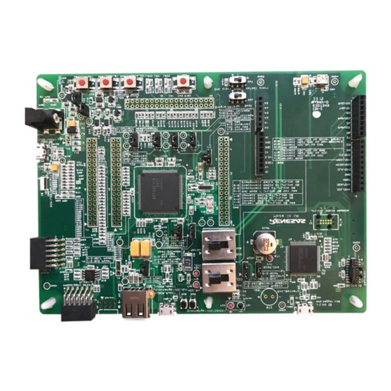
Evaluation Kit RE01 1500KB 3. Board Layout 3. Board Layout Component Layout Figure 3-1, Figure 3-2 below show component layout of Evaluation Kit. Sensor Board Interface J-LINK OB External-Battery Interface PMOD Solar Panel USB Function Connector Host Function Interface (RX621) PMOD2 Slide Switch FLASH MEMORY... -
Page 14: Board Dimensions
Evaluation Kit RE01 1500KB 3. Board Layout Board Dimensions Figure 3-3, Figure 3-4 below show the board dimensions and connector positions. All the through-hole connectors are on a common 2.54mm pitch grid for easy interfacing. USB_2 PMOD2 Sensor USB_1 SCAP Func 5.9mm 54.16mm... - Page 15 Evaluation Kit RE01 1500KB 3. Board Layout MIP-LCD Panel PMOD1 55.0mm 4.0mm phai 12.0mm phai Figure 3-4: MIP-LCD Expansion Board Dimensions R20UT4379EJ0100 Rev. 1.00 Page 15 of 58 Jun 26, 2019...
-
Page 16: Component Placement
Evaluation Kit RE01 1500KB 3. Board Layout Component Placement Figure 3-5, Figure 3-6, Figure 3-7 below show placement of individual components of Evaluation Kit . Component types and values are shown on the board schematics. PMOD2 USB1 USB_2 Sensor1 GND2 USB_1 D1 D2 GND1... - Page 17 Evaluation Kit RE01 1500KB 3. Board Layout R183 R185 R186 R187 R188 R184 R189 R191 R192 R194 R195 R198 R199 R202 R203 R293 R205 R206 R208 R209 R211 R212 R213 R190 R214 R215 R216 R193 R217 R197 R218 R290 R219 R289 R292 R235...
- Page 18 Evaluation Kit RE01 1500KB 3. Board Layout PMOD1 Figure 3-7: MIP-LCD Expansion Board Top-Side Component Placement R20UT4379EJ0100 Rev. 1.00 Page 18 of 58 Jun 26, 2019...
-
Page 19: Connectivity
Evaluation Kit RE01 1500KB 4. Connectivity 4. Connectivity Internal Board Connections The diagram below shows the Evaluation Kit components and their connectivity to the RE01. 5V DC PWR IN (5V) ・AC Adapter ・USB VBUS ・J-Link OB debugger ・I-jet debugger Pow er LED DCDC Converter DCDC Converter Jumper... -
Page 20: Debugger Connections
Evaluation Kit RE01 1500KB 4. Connectivity Debugger Connections 4.2.1 J-Link OB Figure 4-2 shows the connections between Main Board (J-Link OB) and host PC. When J-Link OB is used, disconnect other emulators. USB Cable Main Board Host PC Figure 4-2: Debugger Connection Diagram (J-Link OB) 4.2.2 The Emulators excluding J-Link OB. -
Page 21: User Circuitry
Evaluation Kit RE01 1500KB 5. User Circuitry 5. User Circuitry Reset Circuit A reset control circuit is fitted to the Evaluation Kit to generate the required reset signal, and is triggered from the RES switch. Refer to the RE01 Group User’s Manual: Hardware for details regarding the reset signal timing requirements, and the Evaluation Kit schematics for information regarding the reset circuitry in use on the board. -
Page 22: Potentiometer
Evaluation Kit RE01 1500KB 5. User Circuitry Potentiometer A single-turn potentiometer is connected as a potential divider to analog input AN028 (Port P506, Pin 109). The potentiometer can be used to create a voltage between Board_3V3 and ground. Refer to the manufacturer's website for specification of the potentiometer (Bourns with part number 3314 series). -
Page 23: Pmod
Evaluation Kit RE01 1500KB 5. User Circuitry Pmod™ The CPU board are equipped with connectors for Digilent Pmod™ interface. Please connect the PMOD1, PMOD2 connector that is compatible with PMOD module. The Digilent Pmod™ Compatible headers use an SPI interface. Figure 5-1 below shows Digilent Pmod™ Compatible Header Pin Numbering. -
Page 24: Mip-Lcd Expansion Board Interface
Evaluation Kit RE01 1500KB 5. User Circuitry MIP-LCD Expansion Board Interface Main board has connector for MIP-LCD expansion board interface. Connect MIP-LCD expansion board to PMOD1. PMOD1 is compatible with PMOD module. MIP-LCD (KYOCERA with part number TN0181ANVNANN-AN00 ) loaded on MIP-LCD expansion board uses Serial Peripheral Interface (SPI) built in RE01. -
Page 25: Memory In Pixel Liquid Crystal Display (Mlcd)
Evaluation Kit RE01 1500KB 5. User Circuitry Memory In Pixel Liquid Crystal Display (MLCD) One channel of MIP Liquid Crystal Controller (MLCD) is built in RE01 and can be connected to MIP-LCD (KYOCERA with part number TN0104ANVAANN-GN00 ) through FPC connector (CN3) on main board. The connection of MLCD was shown in Table 5-7. -
Page 26: Universal Serial Bus (Usb)
Evaluation Kit RE01 1500KB 5. User Circuitry 5.12 Universal Serial Bus (USB) This main board is fitted with a USB Host socket (type A) and a Function socket (type Micro B). USB module USB is connected to the Host and Function socket and can operate as either a Host or Function device. The connection for the USB module was shown in Table 5-10 below. -
Page 27: Arduino Uno Interface
Evaluation Kit RE01 1500KB 5. User Circuitry 5.13 Arduino UNO interface This main board is fitted with Arduino UNO interface connector and can be connected to each shield. The connection for the Arduino UNO interface were shown in Table 5-11, Table 5-12, Table 5-13 and Table 5-14 below. -
Page 28: Sensor Board Interface
Evaluation Kit RE01 1500KB 5. User Circuitry 5.14 Sensor board interface This main board is provided with through-hole pattern that can be connected to conventional I2C interface sensor board. The connection for sensor board interface was shown in Table 5-15. Table 5-15: Sensor Board Interface Sensor Board Interface Connector (Sensor1) RE01... -
Page 29: Energy Harvesting Circuit
Evaluation Kit RE01 1500KB 5. User Circuitry 5.15 Energy Harvesting Circuit This main board has an Energy Harvesting (EH) function. By supplying power to port VSC_VCC of RE01 from solar panel, some parts of the board can operate. 5.15.1 Solar Panel The board has two test points where a solar panel can be connected. -
Page 30: Current Measurement Circuit
Evaluation Kit RE01 1500KB 5. User Circuitry 5.15.4 Available User Circuits When using the energy harvesting function, only some user circuits can be used. Available user circuits are LED (LED0-2), switches (SW1, SW2, SW3), PMOD1 (MIP-LCD expansion board), PMOD2, MLCD, flash memory (U2), sensor board interface, Arduino UNO interface. -
Page 31: Configuration
Evaluation Kit RE01 1500KB 6. Configuration 6. Configuration Modifying the Evaluation Kit This section lists the option links that are used to modify the way Evaluation Kit operates in order to access different configurations. Configurations are made by modifying link resistors or headers with movable jumpers or by configuration switches A link resistor is a 0Ω... -
Page 32: Emulators Configuration
Evaluation Kit RE01 1500KB 6. Configuration Emulator Configuration Table 6-2 below details the function of the option links associated with the Emulator’s Configuration. Table 6-2: Emulator Configuration Option Links Settings RE01 RE01 Peripheral Selection Destination Selection Signal Interface name Signal /Function SW6.Pin5 SW6.Pin4... -
Page 33: Power Supply Configuration
Evaluation Kit RE01 1500KB 6. Configuration Power Supply Configuration Table 6-4 below details the function of the option links associated with the Power Supply Configuration. Table 6-4: Power Supply Configuration Option Links Settings Reference Function Related Ref. PWR1 Connect PWR1 to 5V power rail Connect VBUS to Board_5V J13.shorted VBUS... - Page 34 Evaluation Kit RE01 1500KB 6. Configuration Table 6-5 below details the function of the jumpers associated with the Power Supply Configuration. Table 6-5: Power Supply Configuration Jumper Settings Reference Jumper Position Description Related Ref. Connect regulator 3.3V output (UC_VCC) to Shorted Pin1-2 U1, J22 U1(Normal Operation)
-
Page 35: Clock Configuration
Evaluation Kit RE01 1500KB 6. Configuration Clock Configuration Table 6-6 below details the function of the option links associated with Clock Configuration. Table 6-6: Clock Configuration Option Link Settings Related Ref. Reference Description Connect 32MHz crystal (X1) to RE01 R66, R74 XTAL, EXTAL U1.18, U1.19 Disconnect X1 to RE01... - Page 36 Evaluation Kit RE01 1500KB 6. Configuration Table 6-8 below details the function of the jumpers associated with Analog Power & ADC Configuration. Table 6-8: Analog Power & ADC Configuration Jumper Settings Related Ref. Reference Jumper position Description Use external Reference Voltage for 14 bit A/D Shorted Pin1-2 U1, J22, J17 Converter reference voltage...
-
Page 37: General Io & Led Configuration
Evaluation Kit RE01 1500KB 6. Configuration General IO & LED Configuration Table 6-9 below details the function of the option links associated with General IO & LED Configuration. Table 6-9: General IO & LED Configuration Option Links RE01 RE01 Peripheral Setting Destination Selection Signal Interface/... -
Page 38: Pmod1 (Mip-Lcd Expansion Board) Configuration
Evaluation Kit RE01 1500KB 6. Configuration PMOD1 (MIP-LCD Expansion Board) Configuration Table 6-11 below details the function of the option links associated with PMOD1 (MIP-LCD Expansion Board) Configuration. Table 6-11: PMOD1 (MIP-LCD Expansion Board) Configuration Option Links RE01 RE01 Peripheral Setting Destination Selection Signal Interface/... - Page 39 Evaluation Kit RE01 1500KB 6. Configuration Table 6-13: PMOD2 Configuration Option Links (2) RE01 RE01 Peripheral Setting Destination Selection Signal Interface/ name Signal Function QSPI-QSPCLK_A R217 R215, R211 U6.6, R14 PMOD2- P602 P602 RSPCKA_B_QSP R215 R217, R211 PMOD2.4 R176 CLK_A J7-P602 R211 R217,...
-
Page 40: Qspi Configuration
Evaluation Kit RE01 1500KB 6. Configuration 6.11 QSPI Configuration Table 6-14 below details the function of the option links associated with QSPI configuration. Table 6-14: QSPI Configuration Option Links RE01 RE01 Peripheral Setting Destination Selection Signal Interface/ name Signal Function QSPI-QSPCLK_A R217 R215, R211 U6.6, R14... -
Page 41: Usb Serial Configuration
Evaluation Kit RE01 1500KB 6. Configuration 6.12 USB Serial Configuration Table 6-15 below details the function of the option links associated with USB Serial Configuration. Table 6-15: USB Serial Configuration Option Links RE01 RE01 Peripheral Setting Destination Selection Signal Interface/ name Signal Function... -
Page 42: Mlcd Configuration
Evaluation Kit RE01 1500KB 6. Configuration 6.13 MLCD Configuration Table 6-16 below details the function of the option links associated with MLCD Configuration. Table 6-16: MLCD Configuration Option Links RE01 RE01 Peripheral Setting Destination Selection Signal Interface/ name Signal Function CN3.1, CN3.19, R63, MLCD_VCOM R76... -
Page 43: Usb Configuration
Evaluation Kit RE01 1500KB 6. Configuration 6.15 USB Configuration Table 6-18 below details the function of the option links associated with USB Configuration. Table 6-18: USB Configuration Option Links RE01 RE01 Peripheral Setting Destination Selection Signal Interface/ name Signal Function USB_VBUSE R281 R280... -
Page 44: Arduino Uno Configuration
Evaluation Kit RE01 1500KB 6. Configuration 6.16 Arduino UNO Configuration Table 6-20, Table 6-21 below details the function of the option links associated with Arduino UNO Configuration. Table 6-20: Arduino UNO Configuration Option Links (1) RE01 RE01 Peripheral Setting Destination Selection Signal Interface/ name... - Page 45 Evaluation Kit RE01 1500KB 6. Configuration Table 6-21: Arduino UNO Configuration Option Links (2) RE01 RE01 Peripheral Setting Destination Selection Signal Interface/ name Signal Function PMOD2- SSLA0_B_QSSL_ R268 R267, R269 PMOD2.1, R182 R181 P012 P012 ARDUINO- R267 R268, R269 J6.3 SSLA0_B J21-P012 R269...
-
Page 46: Energy Harvesting Configuration
Evaluation Kit RE01 1500KB 6. Configuration 6.17 Energy Harvesting Configuration Table 6-22 ,Table 6-23 below details the function of the option links associated with Energy Harvesting Configuration. Table 6-22: Energy Harvesting Configuration Jumper Option Links (1) Reference Position Jumper Description Related Ref. - Page 47 Evaluation Kit RE01 1500KB 6. Configuration Table 6-23: Energy Harvesting Configuration Jumper Option Links (2) Reference Position Jumper Description Related Ref. Shorted Pin1-2,Pin4- Setting of port VCC_SU, VBAT_EHC, VSC_VCC 5,Pin7-8 when EHC disable (Normal Operation) Shorted Pin2-3,Pin5- Setting of port VCC_SU, VBAT_EHC, VSC_VCC 6,Pin8-9 when EHC enable (EH Operation) Shorted Pin1-2,Pin4-...
-
Page 48: Current Measurement Configuration
Evaluation Kit RE01 1500KB 6. Configuration 6.18 Current Measurement Configuration Table 6-24 below details the function of the jumpers associated with Current Measurement Configuration. Table 6-24: Current Measurement Configuration Jumper Option Links Reference Position Jumper Description Related Ref. Shorted Pin1-2 Set when excluding current measurement. -
Page 49: Headers
Evaluation Kit RE01 1500KB 7. Headers 7. Headers RE01 Headers This Main Board is fitted with RE01 headers, which can be used to observe general IO port. Table 7-1 below lists the connections of the RE01 header, J9. Table 7-1: RE01 Header J9 Connections RE01 Header J9 Function (General IO Function (General IO... - Page 50 Evaluation Kit RE01 1500KB 7. Headers Table 7-2 below lists the connections of the RE01 header, J7. Table 7-2: RE01 Header J7 Connections RE01 Header J7 Function (General IO Function (General IO port/Power) port/Power) RE01 Pin RE01 Pin Circuit Net Name Circuit Net Name P610 P609...
- Page 51 Evaluation Kit RE01 1500KB 7. Headers Table 7-3 below lists the connections of the RE01 header, J8. Table 7-3: RE01 Header J8 Connections RE01 Header J8 Function (General IO Function (General IO port/Power) port/Power) RE01 Pin RE01 Pin Circuit Net Name Circuit Net Name 3.3V 5.0V...
- Page 52 Evaluation Kit RE01 1500KB 7. Headers Table 7-4 below lists the connections of the RE01 header, J21. Table 7-4: RE01 Header J21 Connections RE01 Header J21 Function (General IO Function (General IO port/Power) port/Power) RE01 Pin RE01 Pin Circuit Net Name Circuit Net Name 3.3V 5.0V...
-
Page 53: Code Development
Connect Main Board to PC through Segger development tool J-Link emulator Connect Main Board to PC through Renesas development tool E2 emulator and E2 emulator Lite. For each emulator detail information, refer to each manufacturer's website . Mode Support The RE01 supports Single Chip and Boot Modes (SCI and USB), which are configured on the Evaluation Kit. -
Page 54: Additional Information
Copyright This document may be, wholly or partially, subject to change without notice. All rights reserved. Duplication of this document, either in whole or part is prohibited without the written permission of Renesas Electronics Corporation. © 2018 - 2019 Renesas Electronics Corporation. All rights reserved. - Page 55 RE01 Group REVISION HISTORY Evaluation Kit RE01 1500KB User’s Manual Description Rev. Date Page Summary 1.00 Jun 26, 2019 First Edition issued. C - 1...
- Page 56 RE01 Group Evaluation Kit RE01 1500KB User’s Manual Publication Date: Rev.1.00 Apr 26, 2019 Published by: Renesas Electronics Corporation...
- Page 57 SALES OFFICES Refer to "http://www.renesas.com/" for the latest and detailed information. Renesas Electronics Corporation TOYOSU FORESIA, 3-2-24 Toyosu, Koto-ku, Tokyo 135-0061, Japan Renesas Electronics America Inc. 1001 Murphy Ranch Road, Milpitas, CA 95035, U.S.A. Tel: +1-408-432-8888, Fax: +1-408-434-5351 Renesas Electronics Canada Limited...
- Page 58 RE01 Group R20UT4379EJ0100...
Need help?
Do you have a question about the RE Series and is the answer not in the manual?
Questions and answers