Table of Contents
Advertisement
Quick Links
This user's guide describes the characteristics, operation, and use of the
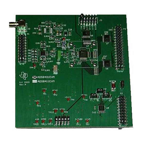
ADS8401/ADS8405/ADS8411 16-bit parallel analog-to-digital converter evaluation
board. A complete circuit description, as well as schematic diagram, layout, and bill of
materials, are included.
1
2
3
4
5
1
2
B-1
B-2
B-3
B-4
1
2
3
4
5
6
7
8
A-1
SLAU114A - December 2004
ADS8401/ADS8405/ADS8411EVM User's Guide
......................................................................................
.....................................................................................
.....................................................................................
......................................................................................
................................................................................
..........................................................................
...........................................................................
..........................................................................
............................................................................
................................................................................
............................................................................
.........................................................................
......................................................................................
Contents
..............................................
..........................................
.....................................
List of Figures
.....................................................................
.............................................
List of Tables
....................................................................
........................................................
.....................................................
....................................................................
ADS8401/ADS8405/ADS8411EVM User's Guide
User's Guide
SLAU114A - December 2004
..................................
2
4
5
6
7
8
10
14
3
7
10
11
12
13
2
3
4
4
4
5
5
6
8
1
Advertisement
Table of Contents

Related Manuals for Texas Instruments ADS8401EVM


Summary of Contents for Texas Instruments ADS8401EVM
-
Page 1: Table Of Contents
Contents ..................EVM Overview ..................Digital Interface ..................Power Supplies ..................Using the EVM ..........Related Documentation From Texas Instruments ........Appendix A ADS8401EVM/ADS8405EVM/ADS8411EVM BOM .......... Appendix B ADS8401/ADS8405/ADS8411EVM Layout ........Appendix C ADS8401/ADS8405/ADS8411EVM Schematic List of Figures .............. -
Page 2: Evm Overview
All odd numbered pins of P1 are tied to AGND. Signal Conditioning The factory recommends the analog input to any SAR type converter be buffered and low pass filtered. This input buffer on the ADS8411/ADS8405/ADS8401EVM utilizes the THS4031 configured as an INVERTING gain of one, as shown in Figure 1. -
Page 3: Ads8411 Input Buffer Circuit
www.ti.com EVM Overview 1kΩ 1kΩ −VCC 0.1 µF 1 µF +4.096 V 15 Ω (+)IN THS4031 10 kΩ 1 µF 6800 pF 500 Ω 0.22 µF 0.1 µF (−)IN +VCC Figure 1. ADS8411 Input Buffer Circuit Reference The ADS8401/ADS8405/ADS8411EVM allows users to select from three different reference sources. It provides an onboard 4.096-V reference circuit. -
Page 4: Digital Interface
Digital Interface Digital Interface The ADS8411/ADS8405/ADS8401EVM is designed for easy interfacing to multiple platforms. Samtec plug and socket connectors provide a convenient dual row header/socket combination at P1, P2 and P3 to plug into prototype boards or ribbon cables. Consult Samtec at www.samtec.com or 1-800-SAMTEC-9 for a variety of mating connector options. -
Page 5: Power Supplies
www.ti.com Power Supplies Table 5. Data Bus Connector P3 (continued) Connector.Pin Signal Description P3.7 Buffered Data Bit 3 P3.9 Buffered Data Bit 4 P3.11 Buffered Data Bit 5 P3.13 Buffered Data Bit 6 P3.15 Buffered Data Bit 7 P3.17 Buffered Data Bit 8 P3.19 Buffered Data Bit 9 P3.21... -
Page 6: Using The Evm
www.ti.com Using the EVM 2. Use the power connector J1, and derive the voltages elsewhere. See Table 8 for the pinouts for this connector. Table 8. Power Connector, J1, Pin Out Signal Power Connector – J1 Signal +VA (+12VA) –VA (–12VA) +AVCC (+5VA) AGND +BVCC (+5VD) -
Page 7: Related Documentation From Texas Instruments
Figure 2. Decoding Control Signals Using the Address Bus Related Documentation From Texas Instruments To obtain a copy of any of the following TI documents, call the Texas Instruments Literature Response Center at (800) 477-8924 or the Product Information Center (PIC) at (972) 644-5580. When ordering, identify this booklet by its title and literature number. -
Page 8: Appendix Aads8401Evm/Ads8405Evm/Ads8411Evm Bom
Appendix A Appendix A ADS8401EVM/ADS8405EVM/ADS8411EVM BOM Table A-1 contains a complete bill of materials for the ADS8401/ADS8405/ADS8411EVM. The schematic diagram is provided in Appendix C. Contact the Product Information Center or e-mail dataconvapps@list.ti.com for questions regarding this EVM. Table A-1. Bill of Materials... - Page 9 TP_0.025 TP1, TP2, TP3, Keystone 5000K-ND Test point - Single, 0.025" pin TP4, TP5, TP6, Electronics TP7, TP8, TP9, TP10, TP11, TP12, TP13, TP14 This part is to be used with the ADS8405EVM only. SLAU114A – December 2004 ADS8401EVM/ADS8405EVM/ADS8411EVM BOM...
-
Page 10: Appendix Bads8401/Ads8405/Ads8411Evm Layout
www.ti.com Appendix B Appendix B ADS8401/ADS8405/ADS8411EVM Layout Figure B-1. Toplayer – Layer 1 ADS8401/ADS8405/ADS8411EVM Layout SLAU114A – December 2004... -
Page 11: Ground Plane - Layer 2
www.ti.com Appendix B Figure B-2. Ground Plane – Layer 2 SLAU114A – December 2004 ADS8401/ADS8405/ADS8411EVM Layout... -
Page 12: Power Plane - Layer 3
www.ti.com Appendix B Figure B-3. Power Plane – Layer 3 ADS8401/ADS8405/ADS8411EVM Layout SLAU114A – December 2004... -
Page 13: Bottom Layer - Layer 4
www.ti.com Appendix B Figure B-4. Bottom Layer – Layer 4 SLAU114A – December 2004 ADS8401/ADS8405/ADS8411EVM Layout... -
Page 14: Appendix Cads8401/Ads8405/Ads8411Evm Schematic
Appendix C Appendix C ADS8401/ADS8405/ADS8411EVM Schematic The following pages contain the schematics for the ADS8401EVM, ADS8405EVM, and ADS8411EVM. ADS8401/ADS8405/ADS8411EVM Schematic SLAU114A – December 2004... - Page 15 Revision History ECN Number Approved Analog-to-Digital Converter 11 12 13 14 15 16 17 18 19 20 EXT_REF Analog Input Power & Digital Buffer B_DB[15...0] TP12 B_DB[15...0] B_DB0 B_DB1 B_DB2 B_DB3 TP14 B_DB4 B_DB5 B_DB6 +AVCC B_DB7 DGND AGND B_DB8 B_DB9 +BVDD TP11...
- Page 16 Revision History +5VCC ECN Number Approved +VCC SJP4 REF3040 0.1uF SJP1 SJP3 EXT_REF 22uF OPA627 B_CS +5VCC +5VCC B_CS B_RD B_RD +5VCC B_CONVST B_CONVST B_BYTE B_BYTE 0.1uF B_RESET B_RESET 0.1uF SJP6 -VCC +VIN VREF 0.01uF 0.1uF BUSY .01uF SJP2 0.1uF 0.01uF +VBD 10uF...
- Page 17 Revision History ECN Number Approved +5VCC +VCC +AVCC BLM21AJ601SN1L BLM21AJ601SN1L 0.1uF 0.01uF 10uF 10uF 47uF 0.01uF 10uF TP13 +VBD 47uF +BVDD 0.01uF 10uF BLM21AJ601SN1L 10uF 0.1uF 0.01uF 10uF BLM21AJ601SN1L -VCC +VBD +VBD 0.1uF DB[17...0] B_RD DB[17...0] B_DB0 +VBD +VBD B_DB1 B_DB2 B_DB3 B_DB4...
- Page 18 EVM IMPORTANT NOTICE Texas Instruments (TI) provides the enclosed product(s) under the following conditions: This evaluation kit being sold by TI is intended for use for ENGINEERING DEVELOPMENT OR EVALUATION PURPOSES ONLY and is not considered by TI to be fit for commercial use.
- Page 19 TI product or service and is an unfair and deceptive business practice. TI is not responsible or liable for any such statements. Following are URLs where you can obtain information on other Texas Instruments products and application solutions:...
Need help?
Do you have a question about the ADS8401EVM and is the answer not in the manual?
Questions and answers