Table of Contents
Advertisement
Quick Links
NUC029KGE
®
®
ARM
Cortex
-M
32-bit Microcontroller
®
NuMicro
Family
NuTiny-SDK-NUC029KGE
User Manual
The information described in this document is the exclusive intellectual property of
Nuvoton Technology Corporation and shall not be reproduced without permission from Nuvoton.
®
Nuvoton is providing this document only for reference purposes of NuMicro
microcontroller based system
design. Nuvoton assumes no responsibility for errors or omissions.
All data and specifications are subject to change without notice.
For additional information or questions, please contact: Nuvoton Technology Corporation.
www.nuvoton.com
Mar 4, 2019
Page 1 of 47
Rev 1.00
Advertisement
Table of Contents

Subscribe to Our Youtube Channel
Related Manuals for Nuvoton NuMicro NuTiny-SDK-NUC029KGE


Summary of Contents for Nuvoton NuMicro NuTiny-SDK-NUC029KGE
- Page 1 NuTiny-SDK-NUC029KGE User Manual The information described in this document is the exclusive intellectual property of Nuvoton Technology Corporation and shall not be reproduced without permission from Nuvoton. ® Nuvoton is providing this document only for reference purposes of NuMicro microcontroller based system design.
-
Page 2: Table Of Contents
NuTiny-SDK-NUC029KGE PCB Placement ............31 How to Start NuTiny-SDK-NUC029KGE on the Keil mdk ENVIRONMENT .... 32 Downloading and Installing Keil MDK Software..........32 Downloading and Installing Nuvoton Nu-Link Driver ..........32 Hardware Setup ..................32 Example Program ..................32 How to Start NuTiny-SDK-NUC029KGE on the IAR Embedded Workbench ..34 Downloading and Installing IAR Embedded Workbench Software ...... - Page 3 NUC029KGE Build and Download Code to NuTiny-SDK-NUC029KGE ..........41 5.3.3 Open the Serial Port Terminal ................41 5.3.4 Reset Chip ..................... 42 5.3.5 NuTiny-SDK-NUC029KGE Schematics ............43 Nu-Link2-Me Schematic ................43 GPIO for 128 pin Schematic ................ 44 Target Chip and SDK Circuit Schematic ............45 REVISION HISTORY ................
-
Page 4: Overview
NUC029KGE OVERVIEW ® NuTiny-SDK-NUC029KGE is a specific development tool for NuMicro NUC029KGE. With the NuTiny-SDK-NUC029KGE, user can develop and verify the application program easily. The NuTiny-SDK-NUC029KGE includes two portions. One is NuTiny-EVB-NUC029KGE and the other is Nu-Link2-Me. NuTiny-EVB-NUC029KGE is the evaluation board and Nu-Link2-Me is its Debug Adaptor. -
Page 5: Nutiny-Sdk-Nuc029Kge Introduction
To use the Nu-Link2-Me Debug adaptor with IAR or Keil, please refer to “Nuvoton NuMicro® IAR ICE driver user manual “or Nuvoton NuMicro® Keil ICE driver user manual” in detail. These two documents will be stored in the local hard disk when the user installs each driver. -
Page 6: Front View
NUC029KGE Front View Figure 2-1 shows the main components and connectors from the front side of NuTiny-SDK- NUC029KGE. The following lists components and connectors from the front view: Off-line Program Button(ICESW1) Extended Connector (JP5, JP4) VCOM Switch ICE Status LED (ICESW2) VDD (JP1) Nu-Link2-Me... -
Page 7: Pin Assignment For Extended Connector
NUC029KGE Pin Assignment for Extended Connector The NuTiny-EVB-NUC029KGE provides NUC029KGE on board and the extended connector (JP3, JP4, JP5 and JP6) for LQFP-128 pin. 128Pin Pin Name Type Description PB.13 General purpose digital I/O pin. ADC0_CH10 ADC0 channel 10 analog input. PB.14 General purpose digital I/O pin. - Page 8 NUC029KGE 128Pin Pin Name Type Description USCI2_CTL1 USCI2 control 1 pin. ACMP0_P0 Analog comparator 0 positive input 0 pin. SC1_DAT Smart Card 1 data pin. EBI_AD4 EBI address/data bus bit 4. nRESET External reset input: active LOW, with an internal pull-up. Set this pin low reset to initial state.
- Page 9 NUC029KGE 128Pin Pin Name Type Description ADC0_CH18 ADC0 channel 18 analog input. UART0_RXD UART0 data receiver input pin. USCI2_CTL0 USCI2 control 0 pin. ACMP1_P3 Analog comparator 1 positive input 3 pin. Timer3 event counter input/toggle output pin. EBI_ALE EBI address latch enable output pin. PD.1 General purpose digital I/O pin.
- Page 10 NUC029KGE 128Pin Pin Name Type Description INT1 External interrupt 1 input pin. PD.4 General purpose digital I/O pin. SPI1_CLK SPI1 serial clock pin. I2C0_SDA C0 data input/output pin. UART2_nRTS UART2 request to Send output pin. PWM0_BRAKE0 PWM0 Brake 0 input pin. Timer0 event counter input/toggle output pin.
- Page 11 NUC029KGE 128Pin Pin Name Type Description USCI2_CTL1 USCI2 control 1 pin. INT5 External interrupt 5 input pin. PF.1 General purpose digital I/O pin. X32_IN External 32.768 kHz crystal input pin. USCI2_CTL0 USCI2 control 0 pin. PWM1_BRAKE0 PWM1 Brake 0 input pin. No connect pin, leave floating.
- Page 12 NUC029KGE 128Pin Pin Name Type Description USCI1_DAT0 USCI1 data 0 pin. SPI1_MISO SPI1 MISO (Master In, Slave Out) pin. UART0_nCTS UART0 clear to Send input pin. PWM1_CH2 PWM1 channel 2 output/capture input. EBI_ADR18 EBI address bus bit 18. PD.15 General purpose digital I/O pin. USCI1_CLK USCI1 clock pin.
- Page 13 NUC029KGE 128Pin Pin Name Type Description No connect pin, leave floating. Power supply for I/O ports and LDO source for internal PLL and digital circuit. No connect pin, leave floating. LDO_CAP LDO output pin. PC.9 General purpose digital I/O pin. SPI0_I2SMCLK SPI0 I2S master clock output pin I2C1_SCL...
- Page 14 NUC029KGE 128Pin Pin Name Type Description SC0_DAT Smart Card 0 data pin. SPI0_CLK SPI0 serial clock pin. UART2_nCTS UART2 clear to Send input pin. USCI0_DAT0 USCI0 data 0 pin. ACMP0_WLAT Analog comparator 0 window latch input pin PWM0_CH0 PWM0 channel 0 output/capture input. EBI_AD8 EBI address/data bus bit 8.
- Page 15 NUC029KGE 128Pin Pin Name Type Description EBI_AD11 EBI address/data bus bit 11. PC.4 General purpose digital I/O pin. SC0_nCD Smart Card 0 card detect pin. SPI0_MISO SPI0 MISO (Master In, Slave Out) pin. I2C1_SCL C1 clock pin. USCI0_CLK USCI0 clock pin. PWM0_CH4 PWM0 channel 4 output/capture input.
- Page 16 NUC029KGE 128Pin Pin Name Type Description ACMP1_O Analog comparator 1 output pin. PWM1_CH0 PWM1 channel 0 output/capture input. EBI_AD14 EBI address/data bus bit 14. PC.7 General purpose digital I/O pin. USCI0_CTL1 USCI0 control 1 pin. PWM1_CH1 PWM1 channel 1 output/capture input. EBI_AD15 EBI address/data bus bit 15.
- Page 17 NUC029KGE 128Pin Pin Name Type Description UART0_TXD UART0 data transmitter output pin. PA.8 General purpose digital I/O pin. CLKO Clock Out I2C1_SCL C1 clock pin. UART1_TXD UART1 data transmitter output pin. SC0_PWR Smart Card 0 power pin. SC1_RST Smart Card 1 reset pin. TM_BRAKE0 TM_BRAKE0 I Timer Brake * input pin.
- Page 18 NUC029KGE 128Pin Pin Name Type Description SPI1_CLK SPI1 serial clock pin. TM0_EXT Timer0 external capture input/toggle output pin. TM_BRAKE1 TM_BRAKE1 I Timer Brake * input pin. EBI_AD7 EBI address/data bus bit 7. PA.6 General purpose digital I/O pin. SPI1_MISO SPI1 MISO (Master In, Slave Out) pin. TM1_EXT Timer1 external capture input/toggle output pin.
- Page 19 NUC029KGE 128Pin Pin Name Type Description SC0_PWR Smart Card 0 power pin. PE.9 General purpose digital I/O pin. UART1_RXD UART1 data receiver input pin. Timer1 event counter input/toggle output pin. I2C1_SDA C1 data input/output pin. SC0_RST Smart Card 0 reset pin. PE.10 General purpose digital I/O pin.
- Page 20 NUC029KGE 128Pin Pin Name Type Description PE.13 General purpose digital I/O pin. SPI1_CLK SPI1 serial clock pin. SPI0_CLK SPI0 serial clock pin. UART1_RXD UART1 data receiver input pin. I2C0_SDA C0 data input/output pin. SPI1_SS SPI1 slave select pin. EBI_AD4 EBI address/data bus bit 4. TM3_EXT Timer3 external capture input/toggle output pin.
- Page 21 NUC029KGE 128Pin Pin Name Type Description I2C0_SDA C0 data input/output pin. SC0_RST Smart Card 0 reset pin. PWM1_CH3 PWM1 channel 3 output/capture input. EBI_AD2 EBI address/data bus bit 2. USCI1_CTL0 USCI1 control 0 pin. PA.1 General purpose digital I/O pin. UART1_nRTS UART1 request to Send output pin.
- Page 22 NUC029KGE 128Pin Pin Name Type Description PA.12 General purpose digital I/O pin. SPI1_I2SMCLK SPI1 I2S master clock output pin UART2_RXD UART2 data receiver input pin. UART1_RXD UART1 data receiver input pin. TM_BRAKE2 TM_BRAKE2 I Timer Brake * input pin. PA.13 General purpose digital I/O pin.
- Page 23 NUC029KGE 128Pin Pin Name Type Description Timer2 event counter input/toggle output pin. USCI1_DAT0 USCI1 data 0 pin. EBI_nWRL EBI low byte write enable output pin. INT1 External interrupt 1 input pin. TM1_EXT Timer1 external capture input/toggle output pin. PB.1 General purpose digital I/O pin. ADC0_CH1 ADC0 channel 1 analog input.
- Page 24 NUC029KGE 128Pin Pin Name Type Description TM_BRAKE1 TM_BRAKE1 I Timer Brake * input pin. EBI_ALE EBI address latch enable output pin. USCI0_DAT1 USCI0 data 1 pin. TM0_EXT Timer0 external capture input/toggle output pin. PB.4 General purpose digital I/O pin. ADC0_CH4 ADC0 channel 4 analog input.
- Page 25 NUC029KGE 128Pin Pin Name Type Description UART1_nRTS UART1 request to Send output pin. TM_BRAKE3 TM_BRAKE3 I Timer Brake * input pin. PWM0_CH2 PWM0 channel 2 output/capture input. USCI0_CTL0 USCI0 control 0 pin. No connect pin, leave floating. Note: Pin Type I = Digital Input, O = Digital Output; AI = Analog Input; P = Power Pin; AP = Analog Power Table 2-1 Pin Assignment for NUC029KGE Mar 4, 2019 Page 25 of 47...
-
Page 26: System Configuration
NUC029KGE System Configuration 2.3.1 5 V Power Sources Table 2-2 presents the 5 V power sources. Net Name in Connector Comment Schematic ICE USB connector supplies 5 V power from PC to ICEJ3 USB_HS_VBUS NUC029KGE platform and Nu-Link2-Me. USB connector on NuTiny-SDK-NUC029KGE supplies USB_VBUS 5 V power from PC to NUC029KGE platform and Nu- Link2-Me. -
Page 27: Usb Connectors
NUC029KGE 2.3.5 USB Connectors Table 2-6 presents the USB connectors. Connector Comment ICE USB connector on Nu-Link2-Me for power supply, debugging and ICEJ3 programming from PC. USB power connector on NuTiny-SDK-NUC029KGE for power supply. Table 2-6 USB Connectors 2.3.6 Power Switches Table 2-7 presents the power switches. - Page 28 NUC029KGE Table 2-8 presents all power models when supplies external power through Nu-Link2-Me. The Nu- Link2-Me external power sources are highlight in yellow. Target ICEJPR1 ICEJPR2 ICE Chip Model Chip ICEJ3 (MCUVCC) (ICEVCC) Voltage Voltage Selection Selection Connect 1.8 V 1.8 V 1.8 V 1.8 V...
- Page 29 NUC029KGE 3. Connect ICEJ3 to PC. 4. Connect the external power supply to JP1. To use JP1 as external power supply source with Nu-Link2-Me separated from NuTiny-SDK- NUC029KGE, please follow the below steps: 1. Separate the Nu-Link2-Me from NuTiny-SDK-NUC029KGE. 2. Connect the external power supply to JP1. To use J2 as external power supply source with Nu-Link2-Me separated from NuTiny-SDK- NUC029KGE, please follow the below steps: 1.
-
Page 30: Extension Connectors
NUC029KGE 2.3.8 Extension Connectors Table 2-10 presents the extension connectors. Connector Comment JP3, JP4, JP5 and JP6 Full pins extension connectors on the NuTiny-SDK-NUC029KGE. Table 2-10 Extension Connectors 2.3.9 Push-Buttons Table 2-11 presents the push buttons. Component Comment ICESW1 Off-line program button to start off-line programming the target chip. Reset button to reset the target chip. -
Page 31: Nutiny-Sdk-Nuc029Kge Pcb Placement
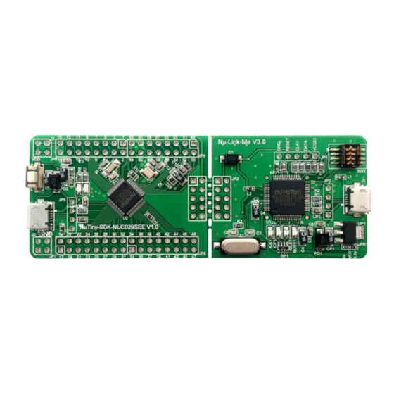
NUC029KGE NuTiny-SDK-NUC029KGE PCB Placement Figure 2-4 shows the NuTiny-SDK-NUC029KGE PCB placement. Figure 2-4 NuTiny-SDK-NUC029KGE PCB Placement Mar 4, 2019 Page 31 of 47 Rev 1.00... -
Page 32: How To Start Nutiny-Sdk-Nuc029Kge On The Keil Mdk Environment
Figure 3-1 NuTiny-SDK-NUC029KGE Hardware Setup Example Program This example demonstrates downloading and debugging an application on a NuTiny-SDK- ® NUC029KGE board. It can be found on the list directory and downloaded from Nuvoton NuMicro website. Mar 4, 2019 Page 32 of 47... - Page 33 NUC029KGE Directory ..\NUC029xGE_BSPv3.00.001\SampleCode\Template\Keil This sample code will show some functions about system manager controller and clock controller. ® Start debug mode Start uVision When using debugger commands, you may: Project – Open Review variables in the watch window Open the SYS.uvproj project file ...
-
Page 34: How To Start Nutiny-Sdk-Nuc029Kge On The Iar Embedded Workbench
Figure 4-1 NuTiny-SDK-NUC029KGE Hardware Setup Example Program This example demonstrates downloading and debugging an application on a NuTiny-SDK- ® NUC029KGE board. It can be found on the list directory and downloaded from Nuvoton NuMicro website. Mar 4, 2019 Page 34 of 47... - Page 35 NUC029KGE Directory ..\NUC029xGE_BSPv3.00.001\SampleCode\Template\IAR This sample code will show some functions about system manager controller and clock controller. Project – Download and Debug Start IAR Embedded Workbench Program the application code into on-chip Flash ROM File-Open-Workspace Open the SYS.eww workspace file Single step through code ...
-
Page 36: Starting To Use Nu-Link2-Me Vcom Function
ICP Programming Tool and Nu-Link USB Driver, which included VCOM driver. Figure 5-1 Optional Step after ICP Programming Tool Installation Figure 5-2 Install Nuvoton COM&LPT Driver Mar 4, 2019 Page 36 of 47 Rev 1.00... - Page 37 NUC029KGE Figure 5-3 Install Nuvoton Universal Serial Bus Controllers Mar 4, 2019 Page 37 of 47 Rev 1.00...
-
Page 38: Vcom Mode Setting On Nutiny-Sdk-Nuc029Kge
NUC029KGE VCOM Mode Setting on NuTiny-SDK-NUC029KGE Before the NuTiny-SDK-NUC029KGE is connected to the PC, please enable VCOM function by switching on ICESW2. The NuTiny-EVB-NUC029KGE transmits through UART0 to VCOM to send out data. Switch ICESW2 off when using UART0 function without VCOM function. Development Tool Setup ®... -
Page 39: Check The Target Device And Debug Setting
NUC029KGE 5.3.2 Check the Target Device and Debug Setting The target device has to be the same as the setting in Debug. Please click “Target Option” to open the Option windows, and find the setting in “Device”, “Debug”, and “Utilities” page. Please follow the steps below to check the setting. - Page 40 NUC029KGE Step 2 Step 3 Mar 4, 2019 Page 40 of 47 Rev 1.00...
-
Page 41: Build And Download Code To Nutiny-Sdk-Nuc029Kge
NUC029KGE 5.3.3 Build and Download Code to NuTiny-SDK-NUC029KGE Please build the project and download code to the NuTiny-SDK-NUC029KGE. 5.3.4 Open the Serial Port Terminal User can use serial port terminal, PuTTY for example, to print out debug message. Figure 5-5 Set Baud Rate Mar 4, 2019 Page 41 of 47 Rev 1.00... -
Page 42: Reset Chip
NUC029KGE 5.3.5 Reset Chip After pushing the reset button, the chip will reprogram application and print out debug message. Figure 5-6 Serial Port Terminal Windows Note: Please switch ICESW2 on before the NuTiny-SDK-NUC029KGE is connected to the PC. When the NuTiny-SDK-NUC029KGE is connected to the PC with ICESW2 switch on, PC will detect VCOM as a USB device and the detection will only be processed once. -
Page 43: Nutiny-Sdk-Nuc029Kge Schematics
NUC029KGE NUTINY-SDK-NUC029KGE SCHEMATICS Nu-Link2-Me Schematic 3.3V ICER1 Off-page Connector 200 1% USB_HS_CAP R0603 ICE5V ICEC1 ICEC2 ICE5V 0.1u MCUVCC_DIODE C0603 C0603 SWDH_DAT TICEDAT SWDH_CLK TICECLK SWDH_RST# TICERST ICE_RX_S MCU_TX ICE_TX_S MCU_RX ICE_RST nRESET ICEVDD VDDIO ETMCK_MOSI PA.0 ETMD0_MISO LDO_CAP PA.1 ICEVDD ETMD2_CK PA.2... -
Page 44: Gpio For 128 Pin Schematic
NUC029KGE GPIO for 128 pin Schematic P1 - P32 P33 - P64 PB13 PB14 PD13 PB15 PD14 PD15 nRESET XT1OUT AVSS XT1IN LDO_CAP PC10 PC11 PC12 PC13 PC14 VBAT X32O X32I PF10 PD11 PD12 HEADER 2.54 16X2 (NC) HEADER 2.54 16X2 (NC) P65 - P96 P97 - P128 USB_VDD33_CAP... -
Page 45: Target Chip And Sdk Circuit Schematic
NUC029KGE Target Chip and SDK Circuit Schematic P1 - P32 P33 - P64 PB13 PD13 PB14 P34_NC PB15 PD14 PD15 nRESET nRESET P39_NC XT1_OUT XT1OUT AVSS XT1_IN AVSS XT1IN P10_NC P42_NC P12_NC P44_NC P46_NC PC.4 LDO_CAP LDO_CAP PC.3 PC.2 PC10 PC.1 PC11 PC.0... -
Page 46: Revision History
NUC029KGE REVISION HISTORY Date Revision Description 2019.03.04 1.00 Initially issued. Mar 4, 2019 Page 46 of 47 Rev 1.00... - Page 47 NUC029KGE Important Notice Nuvoton Products are neither intended nor warranted for usage in systems or equipment, any malfunction or failure of which may cause loss of human life, bodily injury or severe property damage. Such applications are deemed, “Insecure Usage”.
Need help?
Do you have a question about the NuMicro NuTiny-SDK-NUC029KGE and is the answer not in the manual?
Questions and answers