Table of Contents
Advertisement
Quick Links
™
OPTIREG
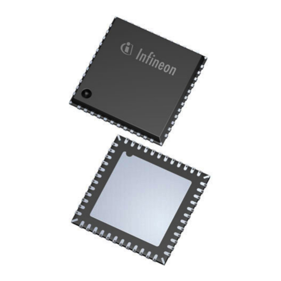
PMIC TLF30681QVS01
Power management IC
Features
•
High-efficiency step-down pre-regulator for wide input voltage range from
3.7 V to 35 V (40 V limited time) with low overall power loss and fast
transient performance
•
Suitable for operation with ceramic capacitors
•
High-efficiency step-down post-regulator for second output voltage
generation
•
Step-up post-regulator with 5 V output voltage
•
Voltage monitoring for two external voltage rails including enable signals
•
16-bit SPI
•
Configurable window watchdog
•
Green Product (RoHS compliant)
Potential applications
•
Automotive applications
•
Advanced Driver Assistance Systems (ADAS)
-
77 GHz radar ECUs
-
Camera ECUs
•
Human Machine Interface (HMI) applications
Product validation
Qualified for automotive applications. Product validation according to AEC-Q100.
Description
™
The OPTIREG
PMIC TLF30681QVS01 is a multiple rail Power Management IC (PMIC) for automotive
applications, optimized for the use in Advanced Driver Assistance Systems (ADAS). The device consists of a
battery connected buck regulator (Buck1) providing 3.3 V to external loads and to two low voltage post-
regulators. The first post-regulator (Buck2) provides an output voltage of 1.25 V (output voltage adjustment via
SPI in the range of 0.9 V to 1.3 V). The second post-regulator (Boost1) provides an output voltage of 5.0 V and is
intended to supply up to two CAN transceivers. The TLF30681QVS01 supports 16-bit SPI communication to a
microcontroller. SPI commands can read status information from the device and control features of the power
regulators, such as PWM synchronization. The device operates at a nominal switching frequency of 2.2 MHz. The
switching frequency is selectable via SPI from 1.8 MHz to 2.5 MHz in steps of 100 kHz. The switching regulators
can synchronize to an external clock signal. The TLF30681QVS01 can provide a synchronization signal for other
DC/DC regulators in the system. The TLF30681QVS01 provides two voltage monitoring channels with
Datasheet
www.infineon.com/OPTIREG-PMIC
Please read the Important Notice and Warnings at the end of this document
Rev. 1.0
2020-04-08
Advertisement
Table of Contents

Related Manuals for Infineon OPTIREG TLF30681QVS01


Summary of Contents for Infineon OPTIREG TLF30681QVS01
-
Page 1: Features
The TLF30681QVS01 can provide a synchronization signal for other DC/DC regulators in the system. The TLF30681QVS01 provides two voltage monitoring channels with Datasheet Please read the Important Notice and Warnings at the end of this document Rev. 1.0 www.infineon.com/OPTIREG-PMIC 2020-04-08... - Page 2 ™ OPTIREG PMIC TLF30681QVS01 Power management IC Description monitoring inputs and enable outputs. The monitoring channels can be used to control and monitor external LDOs or external DC/DC switching regulators. Type Package Marking TLF30681QVS01 PG-VQFN-48 TLF30681 S01 Datasheet Rev. 1.0 2020-04-08...
-
Page 3: Table Of Contents
™ OPTIREG PMIC TLF30681QVS01 Power management IC Table of contents Table of contents Features ................1 Potential applications . - Page 4 ™ OPTIREG PMIC TLF30681QVS01 Power management IC Table of contents Power sequencing and soft start ............38 5.3.1 Electrical characteristics power sequencing and soft start .
- Page 5 ™ OPTIREG PMIC TLF30681QVS01 Power management IC Table of contents SPI registers ................85 SPI register definition .
- Page 6 ™ OPTIREG PMIC TLF30681QVS01 Power management IC Table of contents 9.1.6.7 Register B2VSTAT ..............125 9.1.7 Device information registers .
-
Page 7: Block Diagram
™ OPTIREG PMIC TLF30681QVS01 Power management IC Block diagram Block diagram R1VSx V_S (T30) SYNCI SYNC_In Clock Buck1 Internal SYNCO Generation Driver Supply SYNC_Out Supply Logic R1BTSV R1BTS ENABLE R1SWx SMPR V_Buck1 Buck1 ENABLE Feedback R1PGx R3VS IOVDD R1FB Interface_supply R3SW INTERRUPT Interrupt... -
Page 8: Pin Configuration
™ OPTIREG PMIC TLF30681QVS01 Power management IC Pin configuration Pin configuration Pin assignment SDO 37 24 R2PG2 SDI 38 23 R2PG1 SCL 39 22 R2FB SCS 40 21 AG4 ROT 41 20 R1FB INT 42 19 AG3 Top View WDI 43 18 AG2 17 AG1 TM2 44... -
Page 9: Pin Definitions And Functions Pg-Vqfn-48
™ OPTIREG PMIC TLF30681QVS01 Power management IC Pin configuration Pin definitions and functions PG-VQFN-48 Symbol Function Analog ground, pin 5: Connect this pin directly to ground via a low ohmic and low inductive trace. Not connected: Leave the pin floating in the application. Analog ground, pin 6: Connect this pin directly to ground via a low ohmic and low inductive trace. - Page 10 ™ OPTIREG PMIC TLF30681QVS01 Power management IC Pin configuration Symbol Function R1SW3 High voltage regulator power stage output, pin 3: Connect this pin in parallel with R1SW1 and R1SW2 and then to the pre-regulator output filter inductor. R1BTS Bootstrap supply voltage: Connect this pin via the bootstrap capacitor to the R1SWx pins.
- Page 11 ™ OPTIREG PMIC TLF30681QVS01 Power management IC Pin configuration Symbol Function Test mode 1: Not for customer use. Leave this pin floating in the application. Microcontroller programming mode Connect this pin to ground for normal operation in the application. Optionally the pin can be used for microcontroller programming purposes, see Application information.
- Page 12 ™ OPTIREG PMIC TLF30681QVS01 Power management IC Pin configuration Symbol Function Push-pull output. A "low" pulse at this pin indicates an interrupt, and the microcontroller reads the SPI status registers. Connect this pin to a non-maskable interrupt port (NMI) of the microcontroller. Watchdog input, trigger signal: Connect this pin to the "trigger signal output"...
-
Page 13: General Product Characteristics
™ OPTIREG PMIC TLF30681QVS01 Power management IC General product characteristics General product characteristics Absolute maximum ratings Table 1 Absolute maximum ratings = -40°C to 150°C; all voltages with respect to ground, positive current flowing into pin, (unless otherwise specified) Parameter Symbol Values Unit Note or condition... - Page 14 ™ OPTIREG PMIC TLF30681QVS01 Power management IC General product characteristics Table 1 Absolute maximum ratings (continued) = -40°C to 150°C; all voltages with respect to ground, positive current flowing into pin, (unless otherwise specified) Parameter Symbol Values Unit Note or condition Number Min.
-
Page 15: Functional Range
™ OPTIREG PMIC TLF30681QVS01 Power management IC General product characteristics Table 1 Absolute maximum ratings (continued) = -40°C to 150°C; all voltages with respect to ground, positive current flowing into pin, (unless otherwise specified) Parameter Symbol Values Unit Note or condition Number Min. -
Page 16: Thermal Resistance
™ OPTIREG PMIC TLF30681QVS01 Power management IC General product characteristics Thermal resistance Table 3 Thermal resistance Parameter Symbol Values Unit Note or condition Number Min. Typ. Max. Junction to case – – 12.2 – P_4.3.1 thJC Junction to soldering point 20.1 –... -
Page 17: Quiescent Current
™ OPTIREG PMIC TLF30681QVS01 Power management IC General product characteristics Quiescent current Table 4 Quiescent current = -40°C to 150°C; V = 9 V to 25 V; unless otherwise specified R1VSx Parameter Symbol Values Unit Note or condition Number Min. Typ. -
Page 18: Typical Performance Characteristics Quiescent Current
™ OPTIREG PMIC TLF30681QVS01 Power management IC General product characteristics Typical performance characteristics quiescent current DISABLED state - quiescent current I versus LOCKED state - quiescent current I versus supply voltage V supply voltage V R1VSx R1VSx Datasheet Rev. 1.0 2020-04-08... -
Page 19: Power Converters And Power Management
™ OPTIREG PMIC TLF30681QVS01 Power management IC Power converters and power management Power converters and power management High voltage step-down regulator Buck1 4.1.1 Functional description Buck1 The high-voltage step-down regulator Buck1 converts the battery voltage R1VSx to the Buck1 voltage. A synchronous, current-mode-controlled buck converter with internal power switches is integrated for this purpose. - Page 20 ™ OPTIREG PMIC TLF30681QVS01 Power management IC Power converters and power management Vbat R1VSx R1BTS Bandgap 1 Pre- R1SWx Regulator V_Buck1 Buck1 R1PGx Feedback R1FB Logic SYNCI SYNC_In Clock SYNCO Generation SYNC_Out Figure 3 Functional block diagram Buck1 Modulation concept The converter uses several modulation schemes, depending on the operation mode.
- Page 21 ™ OPTIREG PMIC TLF30681QVS01 Power management IC Power converters and power management If the current in the inductor exceeds the overcurrent protection threshold for a defined time t , then the R1OCP device signalizes an overcurrent timeout event through an interrupt (OCSF1.BUCK1OCW). It is up to the application to decide how to react in this situation, for example by shutting down the converter.
-
Page 22: Electrical Characteristics Buck1
™ OPTIREG PMIC TLF30681QVS01 Power management IC Power converters and power management 4.1.2 Electrical characteristics Buck1 Table 5 Electrical characteristics Buck1 = -40°C to 150°C; V = 3.7 V to 35 V; all voltages with respect to ground, positive current flowing into pin R1VSx (unless otherwise specified) Parameter... - Page 23 ™ OPTIREG PMIC TLF30681QVS01 Power management IC Power converters and power management Table 5 Electrical characteristics Buck1 (continued) = -40°C to 150°C; V = 3.7 V to 35 V; all voltages with respect to ground, positive current flowing into pin R1VSx (unless otherwise specified) Parameter...
-
Page 24: Typical Performance Characteristics Buck1
™ OPTIREG PMIC TLF30681QVS01 Power management IC Power converters and power management 4.1.3 Typical performance characteristics Buck1 Buck1 output voltage V versus Buck1 output voltage V versus R1FB R1FB load current I supply voltage V (drop-out region) R1IOUT R1VSx Datasheet Rev. -
Page 25: Post-Regulator Step-Down Converter Buck2
™ OPTIREG PMIC TLF30681QVS01 Power management IC Power converters and power management Post-regulator step-down converter Buck2 4.2.1 Functional description Buck2 The low-voltage step-down regulator Buck2 converts the output voltage of Buck1 to the VBuck2 voltage. A synchronous, current-mode-controlled buck converter with internal P-/N-MOS power stage is integrated for this purpose. - Page 26 ™ OPTIREG PMIC TLF30681QVS01 Power management IC Power converters and power management The integrated automatic use detection for Buck2 allows the system to tell, whether the application uses Buck2. The device checks the input voltage on the R2VSx pins prior to startup of Buck2. If the pins are connected to the output voltage, then a voltage above the detection threshold is present at the pins and the device assumes that the application requires Buck2.
-
Page 27: Electrical Characteristics Buck2
™ OPTIREG PMIC TLF30681QVS01 Power management IC Power converters and power management 4.2.2 Electrical characteristics Buck2 Table 6 Electrical characteristics Buck2 = -40°C to 150°C; V = 3.7 V to 35 V; all voltages with respect to ground, positive current flowing into pin R1VSx (unless otherwise specified) Parameter... - Page 28 ™ OPTIREG PMIC TLF30681QVS01 Power management IC Power converters and power management Table 6 Electrical characteristics Buck2 (continued) = -40°C to 150°C; V = 3.7 V to 35 V; all voltages with respect to ground, positive current flowing into pin R1VSx (unless otherwise specified) Parameter...
-
Page 29: Typical Performance Characteristics Buck2
™ OPTIREG PMIC TLF30681QVS01 Power management IC Power converters and power management 4.2.3 Typical performance characteristics Buck2 Buck2 output voltage V versus R2FB load current I R2IOUT Datasheet Rev. 1.0 2020-04-08... -
Page 30: Post-Regulator Step-Up Converter Boost1
™ OPTIREG PMIC TLF30681QVS01 Power management IC Power converters and power management Post-regulator step-up converter Boost1 4.3.1 Functional description Boost1 The device integrates a dedicated step-up converter to generate a 5 V output voltage rail from the Buck1 voltage. The converter uses an asynchronous boost topology with internal low-side switch and an external diode. -
Page 31: Electrical Characteristics Boost1
™ OPTIREG PMIC TLF30681QVS01 Power management IC Power converters and power management 4.3.2 Electrical characteristics Boost1 Table 7 Electrical characteristics Boost1 = -40°C to 150°C; V = 3.7 V to 35 V; all voltages with respect to ground, positive current flowing into pin R1VSx (unless otherwise specified) Parameter... -
Page 32: Typical Performance Characteristics Boost1
™ OPTIREG PMIC TLF30681QVS01 Power management IC Power converters and power management 4.3.3 Typical performance characteristics Boost1 Boost1 output voltage V versus R3FB load current I R3IOUT Datasheet Rev. 1.0 2020-04-08... -
Page 33: Support Of External Voltage Rails
™ OPTIREG PMIC TLF30681QVS01 Power management IC Power converters and power management Support of external voltage rails The device supports monitoring of two externally generated voltage rails via voltage monitors. Each voltage monitor consists of an enable pin VMxEN to control the respective regulator and a monitoring input pin VMxFB to monitor the respective voltage rail. -
Page 34: Central Functions
™ OPTIREG PMIC TLF30681QVS01 Power management IC Central functions Central functions Supply voltages The device generates an internal supply voltage from the voltage supplied at the R1VSx pins. This supply voltage R1BTSV power the driver circuit for the power switches of Buck1. R1BTSV cannot be used to supply any external load. -
Page 35: Enable Functionality
™ OPTIREG PMIC TLF30681QVS01 Power management IC Central functions Enable functionality The device features an enable functionality which allows powering up the device using the ENA pin. For example, the ENA pin can be connected to the outside of the ECU or to a wake output of a CAN transceiver. The ENA pin is level-sensitive with a duration-based deglitching. -
Page 36: Electrical Characteristics Enable
™ OPTIREG PMIC TLF30681QVS01 Power management IC Central functions The ENA pin is by default configured to be edge triggered. The device can then only detect an ENA event, if the voltage on the pin rises from "low" to "high". If the configuration of the ENA pin is set to level-sensitive, then the device automatically re-enters the ACTIVE state from any state if the ENA pin is "high". -
Page 37: Typical Performance Characteristics Enable
™ OPTIREG PMIC TLF30681QVS01 Power management IC Central functions 5.2.3 Typical performance characteristics enable ENA pin input voltage thresholds V versus junction temperature T Datasheet Rev. 1.0 2020-04-08... -
Page 38: Power Sequencing And Soft Start
™ OPTIREG PMIC TLF30681QVS01 Power management IC Central functions Power sequencing and soft start The individual output rails are power sequenced to reduce the inrush current during power-up. The device uses a passive power sequencing method where it enables the individual rails when the preceding rail is within its total operating band, that is between the respective undervoltage and overvoltage fault thresholds. - Page 39 ™ OPTIREG PMIC TLF30681QVS01 Power management IC Central functions R1VS or ENA STARTUP BUCK1,UV Actual value BUCK1 BUCK1 BUCK2,UV Actual value BUCK2 BUCK2 BOOST, UV Actual value BOOST1 BOOST1 VM1EN VM1,UV Actual value VM2EN VM2,UV Actual value Startup,Total Figure 5 Power sequencing The device releases the microcontroller reset signal with a configurable delay once the microcontroller supply voltage is within the operating band for a selectable time period DEVCFG0.RESDEL.
-
Page 40: Electrical Characteristics Power Sequencing And Soft Start
™ OPTIREG PMIC TLF30681QVS01 Power management IC Central functions 5.3.1 Electrical characteristics power sequencing and soft start Table 11 Electrical characteristics power sequencing and soft start = -40°C to 150°C; V = 3.7 V to 35 V; all voltages with respect to ground, positive current flowing into pin R1VSx (unless otherwise specified) Parameter... -
Page 41: Frequency Generation And Clock Synchronization
™ OPTIREG PMIC TLF30681QVS01 Power management IC Central functions Frequency generation and clock synchronization The integrated clock generation and a clock manager generate the switching frequencies for the integrated converters. The device support synchronization to an external clock signal as well as generation of the synchronization signal for external circuits. -
Page 42: Electrical Characteristics Frequency Generation And Clock Synchronization
™ OPTIREG PMIC TLF30681QVS01 Power management IC Central functions Synchronization The power converters can be synchronized to an external clock signal (SYNCI) to improve EMC and EMI performance and to reduce cross-talk to the loads. Table 12 shows the specification of the signal. The clock manager synchronizes the switching frequency to this signal according to the configuration in the SPI registers. - Page 43 ™ OPTIREG PMIC TLF30681QVS01 Power management IC Central functions Table 12 Electrical characteristics frequency generation and clock synchronization (continued) = -40°C to 150°C; V = 3.7 V to 35 V; all voltages with respect to ground, positive current flowing into pin R1VSx (unless otherwise specified) Parameter...
-
Page 44: Typical Performance Characteristics Frequency Generation
™ OPTIREG PMIC TLF30681QVS01 Power management IC Central functions 5.4.2 Typical performance characteristics frequency generation Switching frequency f versus MAIN junction temperature T Datasheet Rev. 1.0 2020-04-08... -
Page 45: Iovdd - Overvoltage Detection And Undervoltage Detection
™ OPTIREG PMIC TLF30681QVS01 Power management IC Central functions IOVDD - overvoltage detection and undervoltage detection The IOVDD pin is the supply voltage input for the communication interface towards the microcontroller. The pin can be supplied from one of the voltages generated by the TLF30681QVS01. The TLF30681QVS01 monitors the voltage on the IOVDD pin. - Page 46 ™ OPTIREG PMIC TLF30681QVS01 Power management IC Central functions Table 13 Electrical characteristics IOVDD - overvoltage detection and undervoltage detection (continued) = -40°C to 150°C; V = 3.7 V to 35 V; all voltages with respect to ground, positive current flowing into pin R1VSx (unless otherwise specified) Parameter...
-
Page 47: Monitoring Functions
™ OPTIREG PMIC TLF30681QVS01 Power management IC Monitoring functions Monitoring functions The device incorporates various features for using the device as a supply backbone: • Integrated voltage monitors for the output voltages, see Voltage monitoring • Integrated window watchdog for supervising microcontroller timing, see Window watchdog Voltage monitoring 6.1.1... -
Page 48: Monitoring Of Internal Supply Voltages And Bandgaps
™ OPTIREG PMIC TLF30681QVS01 Power management IC Monitoring functions 6.1.4 Monitoring of internal supply voltages and bandgaps The integrated voltage monitoring function monitors internal supply voltages in order to ensure proper operation. If proper operation can not be ensured, then the device reacts accordingly, see Table The device features two independent voltage references: •... - Page 49 ™ OPTIREG PMIC TLF30681QVS01 Power management IC Monitoring functions Table 14 Electrical characteristics voltage monitoring (continued) = -40°C to 150°C; V = 3.7 V to 35 V; all voltages with respect to ground, positive current flowing into pin R1VSx (unless otherwise specified) Parameter Symbol Values...
-
Page 50: Thermal Protection
™ OPTIREG PMIC TLF30681QVS01 Power management IC Monitoring functions Table 14 Electrical characteristics voltage monitoring (continued) = -40°C to 150°C; V = 3.7 V to 35 V; all voltages with respect to ground, positive current flowing into pin R1VSx (unless otherwise specified) Parameter Symbol Values... -
Page 51: Electrical Characteristics Temperature Sensor Monitoring Block
™ OPTIREG PMIC TLF30681QVS01 Power management IC Monitoring functions A thermal shutdown event (TSD) for any of the three sensors triggers a move to the FAULT state. If a thermal shutdown event occurs, then the device extends the fault time to approximately one second (see Table 27) in order to allow the temperature to drop prior to the restart of the device. -
Page 52: Microcontroller Interface And Supervisory Functions
™ OPTIREG PMIC TLF30681QVS01 Power management IC Microcontroller interface and supervisory functions Microcontroller interface and supervisory functions This section describes the connections between the device and the microcontroller. Figure 8 shows that the microcontroller and the device use several signals for communication and for mutual monitoring of correct operation. - Page 53 ™ OPTIREG PMIC TLF30681QVS01 Power management IC Microcontroller interface and supervisory functions • • SYNCI • SYNCO Datasheet Rev. 1.0 2020-04-08...
-
Page 54: Electrical Characteristics Microcontroller Interface Supply
™ OPTIREG PMIC TLF30681QVS01 Power management IC Microcontroller interface and supervisory functions 7.1.1 Electrical characteristics microcontroller interface supply Table 16 Electrical characteristics microcontroller interface supply = -40°C to 150°C; V = 3.7 V to 35 V; all voltages with respect to ground, positive current flowing into pin R1VSx (unless otherwise specified) Parameter... -
Page 55: Serial Peripheral Interface (Spi)
™ OPTIREG PMIC TLF30681QVS01 Power management IC Microcontroller interface and supervisory functions Serial peripheral interface (SPI) 7.2.1 SPI introduction The serial peripheral interface (SPI) is a synchronous serial data link that operates in full duplex mode. The SDI pin receives data from the microcontroller and the SDO pin transmits data to the microcontroller. The device communicates in slave mode where the master, for example the microcontroller, provides a clock on the SCL pin and initiates the data frame. - Page 56 ™ OPTIREG PMIC TLF30681QVS01 Power management IC Microcontroller interface and supervisory functions • If a parity fault occurs, then the device ignores the data, sets the SPI status bit SPISF.PAR and generates an interrupt. • If a write operation to an invalid address occurs, then the device ignores the data, sets the SPI status SPISF.ADDR and generates an interrupt.
-
Page 57: Spi Write Access To Protected Registers
™ OPTIREG PMIC TLF30681QVS01 Power management IC Microcontroller interface and supervisory functions 7.2.2 SPI write access to protected registers Certain registers are protected against accidental write operations. Those protected registers are implemented in pairs, where a protected register (for example PWDCFG0) is used to store a configuration request, while an associated read-only register (for example RWDCFG0) is used to store the currently active configuration. -
Page 58: Spi Write Initiated State Transition Request And Regulator Configuration
™ OPTIREG PMIC TLF30681QVS01 Power management IC Microcontroller interface and supervisory functions 7.2.3 SPI write initiated state transition request and regulator configuration State machine transitions and configuration of output rails can be performed with direct write access to dedicated registers. A defined protocol protects the registers from unintended changes. In order to request a state transition or a change of the configuration of an output rail the request data must be written to two separate, inverted registers (DEVCTRL... -
Page 59: Spi Timing
™ OPTIREG PMIC TLF30681QVS01 Power management IC Microcontroller interface and supervisory functions 7.2.5 SPI timing A : t D : t G : t J : t M : t P : t SPI_wsclkl SPI_clkr SPI_hi SPI_fl SPI_lag SPI_csr B : t E : t H : t K : t... -
Page 60: Electrical Characteristics Spi
™ OPTIREG PMIC TLF30681QVS01 Power management IC Microcontroller interface and supervisory functions 7.2.6 Electrical characteristics SPI Table 17 Electrical characteristics SPI = -40°C to 150°C; V = 3.7 V to 35 V; all voltages with respect to ground, positive current flowing into pin R1VSx (unless otherwise specified) Parameter... -
Page 61: Electrical Characteristics Spi Timing
™ OPTIREG PMIC TLF30681QVS01 Power management IC Microcontroller interface and supervisory functions 7.2.7 Electrical characteristics SPI timing Table 18 Electrical characteristics SPI timing = -40°C to 150°C; V = 3.7 V to 35 V; all voltages with respect to ground, positive current flowing into pin R1VSx (unless otherwise specified) Parameter... - Page 62 ™ OPTIREG PMIC TLF30681QVS01 Power management IC Microcontroller interface and supervisory functions Table 18 Electrical characteristics SPI timing (continued) = -40°C to 150°C; V = 3.7 V to 35 V; all voltages with respect to ground, positive current flowing into pin R1VSx (unless otherwise specified) Parameter...
-
Page 63: Reset Generation (Rot Signal)
™ OPTIREG PMIC TLF30681QVS01 Power management IC Microcontroller interface and supervisory functions Reset generation (ROT signal) Reset output pin ROT The reset output pin ROT is an open drain structure. As soon as a reset condition occurs, the device pulls the ROT pin below V . -
Page 64: Interrupt Generation (Int Signal)
™ OPTIREG PMIC TLF30681QVS01 Power management IC Microcontroller interface and supervisory functions Interrupt generation (INT signal) A dedicated interrupt generation block is implemented which is handling requests from independent sources to generate an interrupt. The different requesters are as follows: •... - Page 65 ™ OPTIREG PMIC TLF30681QVS01 Power management IC Microcontroller interface and supervisory functions An interrupt is only generated after the reset signal to the microcontroller has been released. An interrupt event which occurred while the reset line for the microcontroller is still active is not signaled at the interrupt line but the particular status bit for this event is set.
-
Page 66: Electrical Characteristics Int
™ OPTIREG PMIC TLF30681QVS01 Power management IC Microcontroller interface and supervisory functions HIGH FSM State ACTIVE Internal interrupt request INTTO INTTO INTTO INTTO HIGH Interrupt line SPI service done HIGH INT not serviced flag (previously set) HIGH INT not serviced flag (previously cleared) Figure 12 Interrupt timing without service in time... - Page 67 ™ OPTIREG PMIC TLF30681QVS01 Power management IC Microcontroller interface and supervisory functions Table 20 Electrical characteristics INT (continued) = -40°C to 150°C; V = 3.7 V to 35 V; all voltages with respect to ground, positive current flowing into pin R1VSx (unless otherwise specified) Parameter...
-
Page 68: Window Watchdog
™ OPTIREG PMIC TLF30681QVS01 Power management IC Microcontroller interface and supervisory functions Window watchdog Principle of operation The integrated window watchdog (WWD) can monitor the microcontroller. The microcontroller monitored must provide periodical triggering during the open windows. Depending on the configuration a trigger event is •... - Page 69 ™ OPTIREG PMIC TLF30681QVS01 Power management IC Microcontroller interface and supervisory functions starts a new long open window without indicating an interrupt. The number of repeated long open windows is limited. If the window watchdog does not recognize valid triggering during the second long open window, then the device generates a hard reset, so it enters FAULT state and it switches off the post regulator output voltages.
- Page 70 ™ OPTIREG PMIC TLF30681QVS01 Power management IC Microcontroller interface and supervisory functions • A trigger during the closed window is invalid WWD triggering. • No trigger during the closed window results in an open window after the closed window. • A trigger during the open window is valid WWD triggering.
-
Page 71: Window Watchdog Timing
™ OPTIREG PMIC TLF30681QVS01 Power management IC Microcontroller interface and supervisory functions 7.5.1 Window watchdog timing Normal operation: correct trigger Long Open Window Closed Window Open Window Closed Window WWDSCMD variable fixed variable fixed immediately immediately Valid WWD triggering Invalid WWD triggering Figure 16 Normal operation: correct trigger If the reset output ROT turns to "high"... - Page 72 ™ OPTIREG PMIC TLF30681QVS01 Power management IC Microcontroller interface and supervisory functions Fault: no trigger during open window after initialization Long Open Window Long Open Window Closed Window WWDSCMD FAULT! variable fixed immediately Valid WWD triggering Invalid WWD triggering Figure 17 Fault operation: No trigger in open window after initialization The initialization timeout usually finishes slightly before or at the same time as the long open window, which skips the interrupt event.
- Page 73 ™ OPTIREG PMIC TLF30681QVS01 Power management IC Microcontroller interface and supervisory functions Fault: no trigger during open window in steady state Open Window Open Window Closed Window Open Window WWDSCMD FAULT! variable fixed variable immediately immediately Valid WWD triggering Invalid WWD triggering Figure 18 Fault operation: no trigger in open window in steady state If the window watchdog does not detect valid triggering during the entire open window, then it...
- Page 74 ™ OPTIREG PMIC TLF30681QVS01 Power management IC Microcontroller interface and supervisory functions Fault: wrong trigger during closed window after initialization Long Open Window Close Open Window Closed Window Open Window WWDSCMD FAULT! variable variable fixed variable immediately immediately immediately immediately Valid WWD triggering Invalid WWD triggering Figure 19...
- Page 75 ™ OPTIREG PMIC TLF30681QVS01 Power management IC Microcontroller interface and supervisory functions Fault: wrong trigger during closed window in steady state Open Window Close Open Window Closed Window Open Window WWDSCMD FAULT! variable variable fixed variable immediately immediately immediately immediately Valid WWD triggering Invalid WWD triggering Figure 20...
-
Page 76: Electrical Characteristics Window Watchdog
™ OPTIREG PMIC TLF30681QVS01 Power management IC Microcontroller interface and supervisory functions 7.5.2 Electrical characteristics window watchdog Table 21 Electrical characteristics window watchdog = -40°C to 150°C; V = 3.7 V to 35 V; all voltages with respect to ground, positive current flowing into pin R1VSx (unless otherwise specified) Parameter... -
Page 77: Electrical Characteristics Microcontroller Programming Mode
™ OPTIREG PMIC TLF30681QVS01 Power management IC Microcontroller interface and supervisory functions 7.6.1 Electrical characteristics microcontroller programming mode Table 22 Electrical characteristics microcontroller programming mode = -40°C to 150°C; V = 3.7 V to 35 V; all voltages with respect to ground, positive current flowing into pin R1VSx (unless otherwise specified) Parameter... -
Page 78: State Machine
™ OPTIREG PMIC TLF30681QVS01 Power management IC State machine State machine State machine introduction The integrated state machine controls operation in different situations. Figure 21 shows the complete state- diagram. Table 23 Table 24 describe each state and the transitions. LOCKED VM1, VM2 Watchdog... -
Page 79: Operation States
™ OPTIREG PMIC TLF30681QVS01 Power management IC State machine Operation states ACTIVE The ACTIVE state is the first state that the device enters after power-on. The device powers up all voltage rails and expects to receive configuration from the microcontroller within the initialization time window according to the INIT timer. - Page 80 ™ OPTIREG PMIC TLF30681QVS01 Power management IC State machine Table 23 Operational states functional overview. (continued) ACTIVE FAULT LOCKED DISABLED Block or function – – – – – – – – – Window watchdog – – – – – – –...
-
Page 81: State Transitions And Trigger Signals
™ OPTIREG PMIC TLF30681QVS01 Power management IC State machine State transitions and trigger signals This section describes the state transitions of the integrated state machine. Table 24 shows the static state transitions with the respective source and destination states, the condition required to trigger the state transition and a transition specific action executed during the transition. - Page 82 ™ OPTIREG PMIC TLF30681QVS01 Power management IC State machine Table 25 Event response mapping – voltage rails (continued) Event Move to Move to Move to No transition; FAULT ACTIVE; DISABLED Generate interrupt Generate RESET Boost1: UV – – – Boost1: StG –...
- Page 83 ™ OPTIREG PMIC TLF30681QVS01 Power management IC State machine Table 26 Event response mapping – other events (continued) Event Move to Move to Move to No transition; FAULT ACTIVE; DISABLED Generate interrupt Generate RESET Buck2: OT warning – – – Buck2: OT fault –...
-
Page 84: Electrical Characteristics State Machine
™ OPTIREG PMIC TLF30681QVS01 Power management IC State machine Move to LOCKED state after third Initialisation Error Device enters LOCKED state after third initialisation error if ENA = LOW HIGH Device enters Fault state after second initialisation error (hard reset event à all FSM State regulator off) ACTIVE... -
Page 85: Spi Registers
™ OPTIREG PMIC TLF30681QVS01 Power management IC SPI registers SPI registers Table 28 Abbreviations Register is reset on a POR event and on a transition into DISABLED state. Register is reset with reset class R0 and additionally on a transition into LOCKED state. Register is reset with reset class R1 and additionally on a microcontroller reset. - Page 86 ™ OPTIREG PMIC TLF30681QVS01 Power management IC SPI registers Table 29 Register overview (continued) Register ID Description Address Reset Reset Page Value Class MONSF0 Voltage monitoring status flags 0 – short to ground Page MONSF1 Voltage monitoring status flags 1 – overvoltage Page MONSF2 Voltage monitoring status flags 2 –...
-
Page 87: Spi Register Definition
™ OPTIREG PMIC TLF30681QVS01 Power management IC SPI registers SPI register definition 9.1.1 Device configuration registers (device startup default configuration) Datasheet Rev. 1.0 2020-04-08... -
Page 88: Register Devcfg0
™ OPTIREG PMIC TLF30681QVS01 Power management IC SPI registers 9.1.1.1 Register DEVCFG0 DEVCFG0 RMAP: 1 Address: Device configuration 0 PAGE: 0 Reset Value: BOOST1EN BUCK2ENA ENA_CONFI VM2ENAS VM1ENAS RESDEL Field Bits Type Description VM2ENAS External voltage monitoring 2 enable at start up , disabled , enabled Reset: 1... -
Page 89: Register Clkcfg0
™ OPTIREG PMIC TLF30681QVS01 Power management IC SPI registers 9.1.1.2 Register CLKCFG0 CLKCFG0 RMAP: X Address: Clock configuration 0 PAGE: 2 Reset Value: PHBUCK2 PHBUCK1 PHSO SSEN SIEN SOEN rwhc Field Bits Type Description Not used PHBUCK2 Buck2 phase alignment , 0°... -
Page 90: Register Clkcfg1
™ OPTIREG PMIC TLF30681QVS01 Power management IC SPI registers 9.1.1.3 Register CLKCFG1 CLKCFG1 RMAP: X Address: Clock configuration 1 PAGE: 2 Reset Value: FREQSEL Field Bits Type Description Not used FREQSEL Main switching frequency , 1.8 MHz , 1.9 MHz , 2.0 MHz , 2.1 MHz , 2.2 MHz... -
Page 91: Register Pwdcfg0
™ OPTIREG PMIC TLF30681QVS01 Power management IC SPI registers 9.1.1.4 Register PWDCFG0 PWDCFG0 RMAP: X Address: Protected watchdog configuration 0 PAGE: 2 Reset Value: WWDETHR WWDEN WWDTSEL WDCYC Field Bits Type Description WWDETHR Window watchdog error threshold Reset: 9 WWDEN Window watchdog enable , disabled , enabled... -
Page 92: Register Pwdcfg1
™ OPTIREG PMIC TLF30681QVS01 Power management IC SPI registers 9.1.1.5 Register PWDCFG1 PWDCFG1 RMAP: X Address: Protected watchdog configuration 1 PAGE: 2 Reset Value: Field Bits Type Description Not used Window watchdog closed window size 0 watchdog cycles 50 watchdog cycles 100 watchdog cycles 6350 watchdog cycles Reset: 46... -
Page 93: Register Pwdcfg2
™ OPTIREG PMIC TLF30681QVS01 Power management IC SPI registers 9.1.1.6 Register PWDCFG2 PWDCFG2 RMAP: X Address: Protected Watchdog Configuration 2 PAGE: 2 Reset Value: Field Bits Type Description Not used Window watchdog open window size 50 watchdog cycles 50 watchdog cycles 100 watchdog cycles 6350 watchdog cycles Reset: 78... -
Page 94: Read-Only Registers For Protected Configuration Registers
™ OPTIREG PMIC TLF30681QVS01 Power management IC SPI registers 9.1.2 Read-only registers for protected configuration registers 9.1.2.1 Register RWDCFG0 RWDCFG0 RMAP: X Address: Read-only watchdog configuration 0 PAGE: 2 Reset Value: WWDETHR WWDEN WWDTSEL WDCYC Field Bits Type Description WWDETHR Window watchdog error threshold ACTIVE Reset: 9 WWDEN... -
Page 95: Register Rwdcfg1
™ OPTIREG PMIC TLF30681QVS01 Power management IC SPI registers 9.1.2.2 Register RWDCFG1 RWDCFG1 RMAP: X Address: Read-only watchdog configuration 1 PAGE: 2 Reset Value: Field Bits Type Description Not used Window watchdog closed window size ACTIVE 0 watchdog cycles 50 watchdog cycles 100 watchdog cycles 6350 watchdog cycles Reset: 46... -
Page 96: Register Rwdcfg2
™ OPTIREG PMIC TLF30681QVS01 Power management IC SPI registers 9.1.2.3 Register RWDCFG2 RWDCFG2 RMAP: X Address: Read-only watchdog configuration 2 PAGE: 2 Reset Value: Field Bits Type Description Not used Window watchdog open window size ACTIVE 50 watchdog cycles 50 watchdog cycles 100 watchdog cycles 6350 watchdog cycles Reset: 78... -
Page 97: Protected Device Configuration Registers
™ OPTIREG PMIC TLF30681QVS01 Power management IC SPI registers 9.1.3 Protected device configuration registers The registers in this section are protected by a defined access procedure. This procedure is based on the access to two individual registers writing inverted information. For detailed information please refer to SPI write initiated state transition request and regulator configuration. -
Page 98: Register Devctrl
™ OPTIREG PMIC TLF30681QVS01 Power management IC SPI registers 9.1.3.1 Register DEVCTRL DEVCTRL RMAP: X Address: Device state control PAGE: 1 Reset Value: VM2EN VM1EN BOOST1EN BUCK2EN STATEREQ Field Bits Type Description VM2EN External voltage monitoring 2 enable request , disable , enable Reset: 0 VM1EN... -
Page 99: Register Devctrln
™ OPTIREG PMIC TLF30681QVS01 Power management IC SPI registers 9.1.3.2 Register DEVCTRLN DEVCTRLN RMAP: X Address: Device state control inverted PAGE: 1 Reset Value: VM2EN VM1EN BOOST1EN BUCK2EN STATEREQ Field Bits Type Description VM2EN External voltage monitoring 2 enable request , enable , disable Reset: 0... -
Page 100: Register B2Vctrl
™ OPTIREG PMIC TLF30681QVS01 Power management IC SPI registers 9.1.3.3 Register B2VCTRL B2VCTRL RMAP: X Address: Buck2 output voltage control PAGE: 1 Reset Value: B2VOUTF rwhu Field Bits Type Description Not used B2VOUTF rwhu Buck2 output voltage setting fine resolution , 1.30 V , 1.20 V , 1.25 V... -
Page 101: Register B2Vctrln
™ OPTIREG PMIC TLF30681QVS01 Power management IC SPI registers 9.1.3.4 Register B2VCTRLN B2VCTRLN RMAP: X Address: Buck2 output voltage control inverted PAGE: 1 Reset Value: B2VOUTF rwhu Field Bits Type Description Not used B2VOUTF rwhu Buck2 output voltage setting fine resolution 1.30 V 1.20 V 1.25 V... -
Page 102: General Registers
™ OPTIREG PMIC TLF30681QVS01 Power management IC SPI registers 9.1.4 General registers 9.1.4.1 Register PROTCFG PROTCFG RMAP: X Address: Configuration protection PAGE: 2 Reset Value: Field Bits Type Description Protection key Reset: 00 Datasheet Rev. 1.0 2020-04-08... -
Page 103: Register Wwdscmd
™ OPTIREG PMIC TLF30681QVS01 Power management IC SPI registers 9.1.4.2 Register WWDSCMD WWDSCMD RMAP: X Address: Window watchdog service command PAGE: 2 Reset Value: TRIG_STAT TRIG Field Bits Type Description TRIG_STATUS Window watchdog last trigger received via SPI Reset: 00 Not used TRIG Window watchdog trigger command... -
Page 104: Event Status Registers
™ OPTIREG PMIC TLF30681QVS01 Power management IC SPI registers 9.1.5 Event status registers The event status registers of the device are organized hierarchically. The global status register is used to collect information of the status flags set in other registers to enable the user to speed up the event source determination. - Page 105 ™ OPTIREG PMIC TLF30681QVS01 Power management IC SPI registers (continued) Field Bits Type Description Reset: 0 rw1c MCU event flag: MCUSF0-QM,MCUSF1-QM , no event, write 0 – no action , event occurred, write 1 to clear the flag Reset: 0 rw1c System event flag: SYSSF0-QM,SYSSF1-QM...
-
Page 106: Register Syssf0
™ OPTIREG PMIC TLF30681QVS01 Power management IC SPI registers 9.1.5.2 Register SYSSF0 SYSSF0-QM RMAP: 1 Address: System status flags – faults PAGE: 0 Reset Value: BGFLT2 BGFLT1 IOVDDOV IOVDDUV FUSEERR rw1c rw1c rw1c rw1c rw1c Field Bits Type Description BGFLT2 rw1c Bandgap fault event 2 , no event, write 0 –... -
Page 107: Register Syssf1
™ OPTIREG PMIC TLF30681QVS01 Power management IC SPI registers 9.1.5.3 Register SYSSF1 SYSSF1-QM RMAP: X Address: System status flags – interrupts PAGE: 1 Reset Value: ENA_PWRU BGWARN2 BGWARN1 SYNC CFG2 rw1c rw1c rw1c rw1c rw1c rw1c rw1c Field Bits Type Description BGWARN2 rw1c... - Page 108 ™ OPTIREG PMIC TLF30681QVS01 Power management IC SPI registers Datasheet Rev. 1.0 2020-04-08...
-
Page 109: Register Mcusf0
™ OPTIREG PMIC TLF30681QVS01 Power management IC SPI registers 9.1.5.4 Register MCUSF0 MCUSF0-QM RMAP: 1 Address: Microcontroller status flags 0 – faults PAGE: 0 Reset Value: HARDRES SOFTRES WWDF INITF rw1c rw1c rw1c rw1c rw1c Field Bits Type Description HARDRES rw1c Hard reset event , no event, write 0 –... -
Page 110: Register Mcusf1
™ OPTIREG PMIC TLF30681QVS01 Power management IC SPI registers 9.1.5.5 Register MCUSF1 MCUSF1-QM RMAP: X Address: Microcontroller status flags 1 – warnings PAGE: 1 Reset Value: WWDMISS rw1c Field Bits Type Description Not used WWDMISS rw1c Window watchdog missed trigger event , no event, write 0 –... -
Page 111: Register Spisf
™ OPTIREG PMIC TLF30681QVS01 Power management IC SPI registers 9.1.5.6 Register SPISF SPISF RMAP: X Address: SPI status flags PAGE: 1 Reset Value: B2VCTRL DEVCTRL LOCK ADDR rw1c rw1c rw1c rw1c rw1c rw1c rw1c Field Bits Type Description Not used B2VCTRL rw1c SPI protocol B2VCTRL access error event... -
Page 112: Register Monsf0
™ OPTIREG PMIC TLF30681QVS01 Power management IC SPI registers 9.1.5.7 Register MONSF0 MONSF0 RMAP: 1 Address: Voltage monitoring status flags 0 – short to ground PAGE: 0 Reset Value: BOOST1ST VM2STG VM1STG BUCK2STG BUCK1STG rw1c rw1c rw1c rw1c rw1c Field Bits Type Description... -
Page 113: Register Monsf1
™ OPTIREG PMIC TLF30681QVS01 Power management IC SPI registers 9.1.5.8 Register MONSF1 MONSF1 RMAP: 1 Address: Voltage monitoring status flags 1 – overvoltage PAGE: 0 Reset Value: VM2OV VM1OV BOOST1OV BUCK2OV BUCK1OV rw1c rw1c rw1c rw1c rw1c Field Bits Type Description VM2OV rw1c... -
Page 114: Register Monsf2
™ OPTIREG PMIC TLF30681QVS01 Power management IC SPI registers 9.1.5.9 Register MONSF2 MONSF2 RMAP: 1 Address: Voltage monitoring status flags 2 – undervoltage PAGE: 0 Reset Value: VM2UV VM1UV BOOST1UV BUCK2UV BUCK1UV rw1c rw1c rw1c rw1c rw1c Field Bits Type Description VM2UV rw1c... -
Page 115: Register Otsf0
™ OPTIREG PMIC TLF30681QVS01 Power management IC SPI registers 9.1.5.10 Register OTSF0 OTSF0 RMAP: 1 Address: Overtemperature events 0 – faults PAGE: 0 Reset Value: MONOT BUCK2OT BUCK1OT rw1c rw1c rw1c Field Bits Type Description MONOT rw1c Monitoring overtemperature fault event , no event, write 0 –... -
Page 116: Register Otsf1
™ OPTIREG PMIC TLF30681QVS01 Power management IC SPI registers 9.1.5.11 Register OTSF1 OTSF1 RMAP: X Address: Overtemperature flags 1 – warnings PAGE: 1 Reset Value: MONOTW BUCK2OTW BUCK1OTW rw1c rw1c rw1c Field Bits Type Description MONOTW rw1c Monitoring overtemperature warning event , no event, write 0 –... -
Page 117: Register Ocsf1
™ OPTIREG PMIC TLF30681QVS01 Power management IC SPI registers 9.1.5.12 Register OCSF1 OCSF1 RMAP: X Address: Overcurrent flags – warnings PAGE: 1 Reset Value: BOOST1OC BUCK2OCW BUCK1OCW rw1c rw1c rw1c Field Bits Type Description Not used BOOST1OCW rw1c Boost1 overcurrent warning event , no event, write 0 –... -
Page 118: Device Status Information Registers
™ OPTIREG PMIC TLF30681QVS01 Power management IC SPI registers 9.1.6 Device status information registers The device status information registers reflect the current status of the device irrespective of the latched status information in the interrupt flag registers. Therefore, reading these registers reflects the current status of the device, for example the currently active power rails or the temperature warnings. -
Page 119: Register Vmonstat0
™ OPTIREG PMIC TLF30681QVS01 Power management IC SPI registers 9.1.6.2 Register VMONSTAT0 VMONSTAT0 RMAP: X Address: Voltage monitoring PAGE: 1 Reset Value: VM2OK VM1OK R1VSxUV BOOST1OK SYNCOK BUCK2OK BUCK1OK Field Bits Type Description VM2OK External voltage monitoring 2 STATUS , output rail disabled or not in total operation band , output rail enabled and in total operation band Reset: 0 VM1OK... - Page 120 ™ OPTIREG PMIC TLF30681QVS01 Power management IC SPI registers Datasheet Rev. 1.0 2020-04-08...
-
Page 121: Register Devstat
™ OPTIREG PMIC TLF30681QVS01 Power management IC SPI registers 9.1.6.3 Register DEVSTAT DEVSTAT RMAP: X Address: Device state information PAGE: 1 Reset Value: VM2EN VM1EN BOOST1EN BUCK2EN STATE Field Bits Type Description VM2EN External voltage monitoring 2 enable STATUS , voltage is disabled , voltage is enabled Reset: 0 VM1EN... -
Page 122: Register Protstat
™ OPTIREG PMIC TLF30681QVS01 Power management IC SPI registers 9.1.6.4 Register PROTSTAT PROTSTAT RMAP: X Address: Protection status information PAGE: 2 Reset Value: KEY4OK KEY3OK KEY2OK KEY1OK LOCK Field Bits Type Description KEY4OK Fourth protection key valid STATUS , key not valid , key valid Reset: 0 KEY3OK... -
Page 123: Register Wwdstat
™ OPTIREG PMIC TLF30681QVS01 Power management IC SPI registers 9.1.6.5 Register WWDSTAT WWDSTAT RMAP: X Address: Window watchdog status information PAGE: 2 Reset Value: WWDECNT Field Bits Type Description Not used WWDECNT Window watchdog error counter level Reset: 0 Datasheet Rev. -
Page 124: Register Mpsstat0
™ OPTIREG PMIC TLF30681QVS01 Power management IC SPI registers 9.1.6.6 Register MPSSTAT0 MPSSTAT0 RMAP: X Address: Microcontroller programming support status PAGE: 1 Reset Value: information MPSSTAT Field Bits Type Description Not used MPSSTAT MPS STATUS , device in operating mode , device in programming mode , device in test mode (production test mode, read-back only) Reset: 3... -
Page 125: Register B2Vstat
™ OPTIREG PMIC TLF30681QVS01 Power management IC SPI registers 9.1.6.7 Register B2VSTAT B2VSTAT RMAP: X Address: Buck2 output voltage status PAGE: 1 Reset Value: BUCK2VOUTC BUCK2VOUTF Field Bits Type Description BUCK2VOUTC Buck2 output voltage setting coarse resolution STATUS , Range 0.9 – 1.3 V. Fine resolution is evaluated. , 1.5 V , 1.8 V , 2.45 V... -
Page 126: Device Information Registers
™ OPTIREG PMIC TLF30681QVS01 Power management IC SPI registers 9.1.7 Device information registers Datasheet Rev. 1.0 2020-04-08... -
Page 127: Register Hwdect0
™ OPTIREG PMIC TLF30681QVS01 Power management IC SPI registers 9.1.7.1 Register HWDECT0 HWDECT0 RMAP: X Address: Hardware option information PAGE: 1 Reset Value: BOOST1AV VM2AVA VM1AVA BUCK2AVA Field Bits Type Description VM2AVA External voltage monitoring 2 automatic use detection , VM2 is not used in this application. , VM2 is used in this application. -
Page 128: Register Devid
™ OPTIREG PMIC TLF30681QVS01 Power management IC SPI registers 9.1.7.2 Register DEVID DEVID RMAP: X Address: Device identification PAGE: 1 Reset Value: DEVTYPE Field Bits Type Description DEVTYPE Device family , TLF30681 device Reset: 30 Datasheet Rev. 1.0 2020-04-08... -
Page 129: Application Information
™ OPTIREG PMIC TLF30681QVS01 Power management IC Application information Application information Note: The following information is given as an example for the implementation of the device only and shall not be regarded as a description or warranty of a certain functionality, condition or quality of the device. - Page 130 Use a ceramic capacitor in X7R material with a voltage rating of 10 V or higher. 10 µF Boost1 output capacitor 2: Boost1_2 Use a ceramic capacitor in X7R material with a voltage rating of 10 V or higher. For additional supportive documentation or further information please contact http://www.infineon.com/. Datasheet Rev. 1.0 2020-04-08...
-
Page 131: Package Information
To meet the world-wide customer requirements for environmentally friendly products and to be compliant with government regulations the device is available as a green product. Green products are RoHS-Compliant (Pb- free finish on leads and suitable for Pb-free soldering according to IPC/JEDEC J-STD-020). Information on alternative packages Please visit www.infineon.com/packages. Datasheet Rev. 1.0 2020-04-08... -
Page 132: Revision History
™ OPTIREG PMIC TLF30681QVS01 Power management IC Revision history Revision history Revision Date Changes 2020-04-08 Datasheet created. Datasheet Rev. 1.0 2020-04-08... -
Page 133: Disclaimer
Infineon Technologies, All Rights Reserved. any kind, including without limitation warranties of Infineon Technologies’ products may not be used in non-infringement of intellectual property rights of any any applications where a failure of the product or third party.
Need help?
Do you have a question about the OPTIREG TLF30681QVS01 and is the answer not in the manual?
Questions and answers