Table of Contents
Advertisement
Quick Links
EVK-NINA-W1/EVK-NINA-B2
Evaluation kit for NINA-W1 and NINA-B2 modules
User guide
Abstract
This document describes how to set up the EVK-NINA-W1/EVK-NINA-B2 evaluation kits to evaluate
NINA-W1 series and NINA-B2 series stand-alone modules. It also describes the different options for
debugging and the development capabilities included in the evaluation board.
UBX-17011007 - R08
C1-Public
www.u-blox.com
Advertisement
Table of Contents

Related Manuals for Ublox EVK-NINA-W1


Summary of Contents for Ublox EVK-NINA-W1
- Page 1 User guide Abstract This document describes how to set up the EVK-NINA-W1/EVK-NINA-B2 evaluation kits to evaluate NINA-W1 series and NINA-B2 series stand-alone modules. It also describes the different options for debugging and the development capabilities included in the evaluation board.
-
Page 2: Document Information
EVK-NINA-W1/EVK-NINA-B2 - User guide Document information Title EVK-NINA-W1/EVK-NINA-B2 Subtitle Evaluation kit for NINA-W1 and NINA-B2 modules Document type User guide Document number UBX-17011007 Revision and date 17-Jul-2020 Disclosure restriction C1-Public This document applies to the following products: Product name Software version... -
Page 3: Table Of Contents
EVK-NINA-W1/EVK-NINA-B2 - User guide Contents Document information ..........................2 Contents ................................3 Product description ..........................4 1.1 Overview ................................ 4 1.2 Kit includes ..............................6 1.2.1 EVK-NINA-B221 and EVK-NINA-W1x1 ..................6 1.2.2 EVK-NINA-B222 and EVK-NINA-W1x2 ..................6 1.2.3 EVK-NINA-W1x6 ..........................6 1.3 I/O allocation.............................. -
Page 4: Product Description
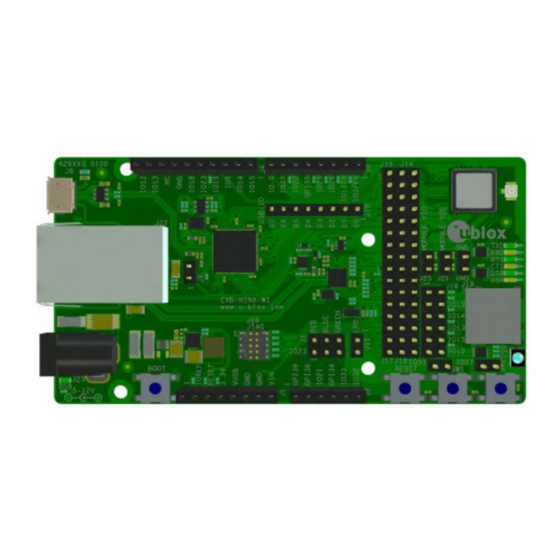
Product description 1.1 Overview The EVK-NINA-W1/EVK-NINA-B2 evaluation kit includes an evaluation board, which can be used as a reference design for the NINA-W1 or NINA-B2 series modules, a quick start guide, and a USB cable. For the NINA-B221 and the NINA-W1x1 module, the evaluation board is prepared with a U.FL coaxial connector for connecting the external antenna. - Page 5 EVK-NINA-W1/EVK-NINA-B2 - User guide Figure 1: EVK-NINA-W1x1/ EVK-NINA-B2x1 evaluation board with U.FL connector for external antenna Figure 2: EVK-NINA-W1x2/ EVK-NINA-B2x2 evaluation board with onboard PIFA antenna ⚠ Take care while handling the EVK-NINA-B222 and EVK-NINA-W1x2. Applying force to the NINA module might damage the internal PIFA antenna.
-
Page 6: Kit Includes
EVK-NINA-W1/EVK-NINA-B2 - User guide Figure 3: EVK-NINA-W1x6 evaluation board with internal PCB trace antenna 1.2 Kit includes 1.2.1 EVK-NINA-B221 and EVK-NINA-W1x1 The EVK-NINA-B221 and EVK-NINA-W1x1 evaluation kits include the following: • EVK-NINA-B221 or EVK-NINA-W1x1 evaluation board • 2.4 GHz foldable antenna (Ex-It 2400) with reverse polarity SMA connector •... -
Page 7: I/O Allocation
EVK-NINA-W1/EVK-NINA-B2 - User guide 1.3 I/O allocation The block diagram in Figure 4 provides a better understanding of how I/O signals from the module are made available at connectors and/or interfaces of the EVK. Sixteen (16) I/O signals (on EVK-NINA-W1x6 17 signals) are available at the middle row of the I/O allocator. -
Page 8: Jumper Description
Connects EVK internal 3.3 V to module pin-9 to supply module VCC_IO Enable VCC Connects EVK internal 3.3 V to modle pin-10 to supply module VCC Table 1: EVK-NINA-W1/EVK-NINA-B2 jumper descriptions J15 (pin-1) J14 (pin-1) J26 (pin-1) J16 (pin-1) - Page 9 EVK-NINA-W1/EVK-NINA-B2 - User guide Middle row jumper pin Connected to J16-1 Module pin-8 J16-3 Module pin-27 J16-5 Module pin-25 J16-7 Module pin-24 J16-9 Module pin-31 J16-11 Module pin-35 J16-13 Module pin-32 J16-15 Module pin-36 Table 2: Available module pins at the middle row of jumpers J14 and J16...
-
Page 10: Default Jumper Configuration
EVK-NINA-W1/EVK-NINA-B2 - User guide 1.4.1 Default jumper configuration Mod pin-21 to J18-3 Mod pin-20 to IO22 (RTS) Mod pin-16 to IO25 (DTR) Mod pin-28 to IO5 Mod pin-17 to IO26 (DSR) Mod pin-29 to IO18 3.3V to Mod pin-9 Mod pin-18 to IO27 3.3V to Mod pin-10... -
Page 11: Leds
EVK-NINA-W1/EVK-NINA-B2 - User guide 1.5 LEDs Figure 8: Position of LEDs on EVK-NINA-W1/EVK-NINA-B2. The SD card slot is move to the bottom side and the DS2-DS7 LEDs are moved closer to DS9 on EVB-NINA-W1x6 Function Description Name Color Power LED Supplied from the EVK 3.3 V DC/DC converter... -
Page 12: Connectors
The available connectors on the EVK-NINA-W1/EVK-NINA-B2 board are shown in Figure 10. * Available on EVK-NINA-W1x6 Figure 10: EVK-NINA-W1/EVK-NINA-B2 connectors. The SD card slot is on the bottom side and the DS2-DS7 LEDs are moved closer to DS9 on EVB-NINA-W1x6. J25-J26 have swapped positon with the module on the EVB-NINA-W1x6 board. -
Page 13: Configuration Options
USB connector, and all control must subsequently be done through the J3 and J4 connectors. 1.8.2 Power supply The supply voltage to the EVK-NINA-W1/EVK-NINA-B2 evaluation board can be sourced from the following connectors: • USB (J8) ☞... -
Page 14: Setting Up The Evaluation Board
EVK-NINA-W1/EVK-NINA-B2 - User guide Setting up the evaluation board The EVK-NINA-W10 is delivered without any software (open CPU) and the software must be developed by the user. The EVK-NINA-B2, EVK-NINA-W13, and EVK-NINA-W15 are delivered with the u-blox connectivity software pre-flashed on the module. -
Page 15: Starting Up
EVK-NINA-W1/EVK-NINA-B2 - User guide • EVK-NINA-B222 • EVK-NINA-W131 • EVK-NINA-W132 • EVK-NINA-W151 • EVK-NINA-W152 • EVK-NINA-W156 2.2.1 Starting up Perform the following steps to enable communication with the module: Start the u-blox s-center evaluation software. Use the default baud rate 115200, 8N1 with flow control. Now, it is possible to communicate with the module through AT commands. -
Page 16: Appendix
EVK-NINA-W1/EVK-NINA-B2 - User guide Appendix A Layout EVK-NINA-W1x1, -W1x2 and EVK-NINA-B221, -B222 R 2 0 J 1 5 J 1 4 J 2 1 R 1 7 R 1 8 C 1 0 R 1 9 J 1 0 R 1 3... -
Page 17: C Schematic Drawing Evk-Nina-W1X1, -W1X2 And Evk-Nina-B221, -B222
EVK-NINA-W1/EVK-NINA-B2 - User guide C Schematic drawing EVK-NINA-W1x1, -W1x2 and EVK-NINA-B221, -B222 UBX-17011007 - R08 Appendix Page 17 of 27 C1-Public... - Page 18 EVK-NINA-W1/EVK-NINA-B2 - User guide UBX-17011007 - R08 Appendix Page 18 of 27 C1-Public...
- Page 19 EVK-NINA-W1/EVK-NINA-B2 - User guide UBX-17011007 - R08 Appendix Page 19 of 27 C1-Public...
- Page 20 EVK-NINA-W1/EVK-NINA-B2 - User guide UBX-17011007 - R08 Appendix Page 20 of 27 C1-Public...
-
Page 21: D Schematic Drawing Evk-Nina-W1X6
EVK-NINA-W1/EVK-NINA-B2 - User guide D Schematic drawing EVK-NINA-W1x6 UBX-17011007 - R08 Appendix Page 21 of 27 C1-Public... - Page 22 EVK-NINA-W1/EVK-NINA-B2 - User guide UBX-17011007 - R08 Appendix Page 22 of 27 C1-Public...
- Page 23 EVK-NINA-W1/EVK-NINA-B2 - User guide UBX-17011007 - R08 Appendix Page 23 of 27 C1-Public...
- Page 24 EVK-NINA-W1/EVK-NINA-B2 - User guide UBX-17011007 - R08 Appendix Page 24 of 27 C1-Public...
-
Page 25: E Glossary
EVK-NINA-W1/EVK-NINA-B2 - User guide Figure 13: Schematic drawings of EVK-NINA-W1x6. E Glossary Name Definition Communication Clear to send Data set ready Data terminal ready Evaluation kit Ground General purpose input GPIO General Purpose Input/Output Input-output Light-Emitting Diode Physical layer U.FL... -
Page 26: Related Documents
EVK-NINA-W1/EVK-NINA-B2 - User guide Related documents NINA-W10 data sheet, doc. no. UBX-17065507 NINA-W13 data sheet, doc. no. UBX-17006694 NINA-W15 data sheet, doc. no. UBX-18006647 NINA-B2 data sheet, doc. no. UBX-18006649 u-connect AT commands manual, doc. no. UBX-14044127 FTDI FT4232H QUAD HIGH SPEED USB TO MULTIPURPOSE UART/MPSSE IC Datasheet - http://www.ftdichip.com/Support/Documents/DataSheets/ICs/DS_FT4232H.pdf... -
Page 27: Contact
EVK-NINA-W1/EVK-NINA-B2 - User guide Contact For complete contact information, visit us at www.u-blox.com. u-blox Offices North, Central and South America Headquarters Asia, Australia, Pacific Europe, Middle East, Africa u-blox America, Inc. u-blox Singapore Pte. Ltd. u-blox AG Phone: +1 703 483 3180...
Need help?
Do you have a question about the EVK-NINA-W1 and is the answer not in the manual?
Questions and answers