Tektronix TriMode P7700 Series Technical Reference
Probes
Hide thumbs
Also See for TriMode P7700 Series:
- User manual (56 pages) ,
- Installation and safety instructions (12 pages) ,
- Quick manual (4 pages)
Table of Contents
Advertisement
Quick Links
Advertisement
Table of Contents

Related Manuals for Tektronix TriMode P7700 Series


Summary of Contents for Tektronix TriMode P7700 Series
- Page 1 P7700 Series TriMode™ Probes Technical Reference *P077112401* 077-1124-01...
- Page 3 P7700 Series TriMode™ Probes Technical Reference www.tek.com 077-1124-01...
- Page 4 Copyright © Tektronix. All rights reserved. Licensed software products are owned by Tektronix or its subsidiaries or suppliers, and are protected by national copyright laws and international treaty provisions. Tektronix products are covered by U.S. and foreign patents, issued and pending. Information in this publication supersedes that in all previously published material.
- Page 5 Tektronix, with shipping charges prepaid. Tektronix shall pay for the return of the product to Customer if the shipment is to a location within the country in which the Tektronix service center is located. Customer shall be responsible for paying all shipping charges, duties, taxes, and any other charges for products returned to any other locations.
-
Page 7: Table Of Contents
Table of Contents Important safety information ..................General safety summary ..................Terms in this manual ..................Symbols and terms on the product ................Theory of operation ....................Introduction..................... TriMode operation .................... Operating voltages .................... Improving measurement accuracy ................Reference ......................Single-ended measurements ................. - Page 8 Table of Contents List of Figures Figure 1: P7700 Series TriMode probe components ............Figure 2: P7700 Series TriMode active probe tips.............. Figure 3: P7700 Series TriMode probe input architecture ............. Figure 4: TriMode input structure ................Figure 5: P7700 probe tip inputs................. Figure 6: Operating voltage window (TekFlex solder-in tips)..........
- Page 9 Table of Contents List of Tables Table 1: Probe tip attenuation factors ................Table 2: Rise time and overshoot degradation versus lead length ........... Table 3: Single-ended dynamic and offset ranges ............. Table 4: Electrical characteristics................Table 5: Environmental characteristics ................. Table 6: Typical electrical characteristics...............
-
Page 10: Important Safety Information
Important safety information Important safety information This manual contains information and warnings that must be followed by the user for safe operation and to keep the product in a safe condition. General safety summary Use the product only as specified. Review the following safety precautions to avoid injury and prevent damage to this product or any products connected to it. -
Page 11: Terms In This Manual
Important safety information Terms in this manual These terms may appear in this manual: WARNING. Warning statements identify conditions or practices that could result in injury or loss of life. CAUTION. Caution statements identify conditions or practices that could result in damage to this product or other property. - Page 12 Important safety information P7700 Series TriMode Probes Technical Reference...
-
Page 13: Theory Of Operation
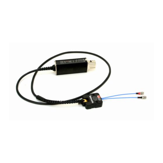
Theory of operation Introduction The P7700 Series TriMode Probes are designed for use with MSO/DPO70000C and newer oscilloscopes. Four P7700 Series TriMode Probe models are available with bandwidths from 8 GHz to 20 GHz. MSO/DPO70000C oscilloscope models are available at comparable bandwidths. These probe and oscilloscope models feature the high performance TekConnect intelligent probe interface. - Page 14 Theory of operation Probe components P7700 Series probes are comprised of a probe compensation box (comp box), a TekFlex connector for attaching probe tips, and an interconnect cable that transfers measured signals, power, and control signals between the probe comp box and the TekFlex connector probe head.
- Page 15 Theory of operation TekFlex™ connector. The new TekFlex connector technology combines a high speed signal path with low speed control signaling in a single, easy to connect accessory connector. The TekFlex connector has a pinch-to-open design that when open requires minimal force to attach an accessory tip. When the TekFlex connector is closed, it provides a secure connection to the accessory to avoid accidental disconnections.
-
Page 16: Figure 2: P7700 Series Trimode Active Probe Tips
The browser tip can be held in place or can be used to make hands-free connections to the DUT when using the Browser Tri-Pod accessory, or a probe positioner, such as the Tektronix PPM203B. The browser includes multiple sets of S-parameters based on the spacing of the tips. The spacing is monitored and the correct set of S-parameters are automatically used. -
Page 17: Figure 3: P7700 Series Trimode Probe Input Architecture
Theory of operation Probe input architecture P7700 Series probes feature a new probe architecture that addresses the need for high frequency response with decreased probe loading for high-speed, low power applications such as MIPI® and LPDDR. High performance probes with multi-GHz bandwidth have evolved in recent years, starting from traditional designs with metal pin tips attached to a probe head amplifier located at the end of a coaxial cable. -
Page 18: Table 1: Probe Tip Attenuation Factors
Theory of operation The P7700 Series active probe tip has two inputs, A_IN and B_IN, which can, depending on the tip design, support TriMode measurements. With a TriMode tip, such as a TekFlex solder-in tip, it is possible to make differential, single-ended A, single-ended B, and common-mode measurements, all from a single soldered differential signal connection to a DUT. - Page 19 Theory of operation The control features of the new TekFlex interface include two analog tip offset voltage signals, a pair of digital communication signals for accessing the probe tip S-parameter memory, and a probe tip temperature monitor signal. The probe tip S-parameter memory contains characterization data for use with DSP correction filters that are unique to the probe tip.
- Page 20 A input to the signal and the ground input of the probe to the ground input of the DUT. In this situation, Tektronix recommends using A-B mode with the B input connected to ground. Reasons for this recommendation...
- Page 21 Theory of operation The downloaded S-parameter data for a probe and attached probe tip is used by the oscilloscope to generate a DSP correction filter for optimum measurement fidelity. Because this S-parameter data is unique and serialized for each probe and probe tip, it only needs to be downloaded once to an oscilloscope.
-
Page 22: Trimode Operation
Theory of operation TriMode operation The TriMode feature of the P7700 Series probes is designed for improved convenience and enhanced capability in measuring differential signal quality. Because a differential signal is composed of two complementary single-ended signals, full characterization of a differential signal requires more than a simple differential measurement. -
Page 23: Figure 4: Trimode Input Structure
Theory of operation The four input amplifiers are multiplexed together and only the selected input mode function is sent to the connected oscilloscope. The following figure shows a conceptual view of the TriMode probe input structure, where the C input provides the probe ground reference and is connected to the probe tip ground interconnect using the probe’s cable coaxial shields. -
Page 24: Operating Voltages
Theory of operation Operating voltages The P7700 Series probes are designed to probe high-frequency, low-voltage circuits. Before probing a circuit, take into account the limits for the operating voltages discussed in this section. Input voltage Operating voltage window Input signal dynamic range Offset voltage Figure 5: P7700 probe tip inputs P7700 Series TriMode Probes Technical Reference... -
Page 25: Figure 6: Operating Voltage Window (Tekflex Solder-In Tips)
Theory of operation Input voltage The maximum input voltage is the maximum voltage to ground that the inputs can withstand without damaging the probe input circuitry. The P7700 Series active probe tips include some over-voltage protection circuitry at the probe tip signal inputs. - Page 26 Theory of operation The dynamic range square (labeled Small Signal AC in the previous figure) can be moved around within the limits of the operating voltage window by adjusting the A and B offset voltage settings. The A and B offset voltage values determine the location of the center of the dynamic range square in the operating voltage window plot.
-
Page 27: Figure 7: Dynamic Range Versus Linearity At The Probe Amplifier Step Gain Settings
Theory of operation Figure 7: Dynamic range versus linearity at the probe amplifier step gain settings The size of the operating voltage window and the size of the full dynamic range for a P7700 Series probe tip depend on the attenuation factor of the input attenuation network at the probe tip. -
Page 28: Figure 8: Operating Voltage Window (P77Brwsr)
Theory of operation Figure 8: Operating voltage window (P77BRWSR) Input signal dynamic range The input signal dynamic range is the maximum voltage difference between the A and B inputs of the probe tip and the probe tip ground reference that the probe can accept without distorting the signal. - Page 29 Theory of operation The dynamic range of P7700 Series probe tips is specified with a linearity error limit of ±1%. As shown in the Linearity Error plot, the linearity error increases as the input voltage increases above the dynamic range limit for both signal polarities.
-
Page 30: Figure 10: Simplified Diagram Of The P7700 Series Probe Tip Input Network
Theory of operation Offset voltage The offset voltage control sums an adjustable DC voltage with the probe signal input. It is commonly used to nullify an input DC bias voltage to center the input signal swing within the linear dynamic range of the probe input. The A and B probe inputs both have an independent offset voltage control. -
Page 31: Figure 11: Probe Setup Screen
Theory of operation There are four manual offset voltage value entry fields which also display the current offset voltage settings. Although all four offset voltage value entry fields are active, only two of the control pairs are independent. The manual controls interact with each other as follows: Adjusting the A or B settings affects the Differential and Common settings: Differential = (A –... -
Page 32: Figure 12: Simplified Auto Offset Circuitry
Theory of operation Figure 12: Simplified Auto Offset circuitry The A and B input signals are buffered by the active probe tip buffer amplifier and passed down the probe main cable assembly into the comp box probe amplifier input pins. The A and B input signals are picked off inside the probe amplifier with large value resistors and output to an averaging filter capacitor as Sense_A and Sense_B signals. -
Page 33: Improving Measurement Accuracy
Theory of operation Improving measurement accuracy DSP correction filtering P7700 Series probes and probe tips use DSP correction filtering to optimize probe measurement fidelity. High frequency time domain measurement performance characteristics such as rise time, aberrations, and pulse flatness are improved by DSP correction filtering. - Page 34 DC Gain and Output Zero performance. The DC probe calibration operation uses a standard accessory test fixture (Tektronix part number, 067-4889-00) that automates the process. The calibration process uses a programmable DC voltage source available on the oscilloscope front panel.
-
Page 35: Figure 13: P77Stflxa Solder Tip Attached With 10 Mils (0.250 Mm) Wires (Rise Time = 30.5 Ps)
Theory of operation The typical pulse waveforms in the following figures show the effect of input wire length variation on measured responses. Figure 13: P77STFLXA solder tip attached with 10 mils (0.250 mm) wires (rise time = 30.5 ps) Figure 14: P77STFLXA solder tip attached with 75 mils (1.90 mm) wires (rise time = 27.9 ps) P7700 Series TriMode Probes Technical Reference... -
Page 36: Figure 15: P77Stflxa Solder Tip Attached With 120 Mils (3.05 Mm) Wires (Rise Time = 30.1 Ps)
Theory of operation Figure 15: P77STFLXA solder tip attached with 120 mils (3.05 mm) wires (rise time = 30.1 ps) Figure 16: P77STFLXA solder tip attached with 200 mils (5.08 mm) wires (rise time = 34 ps) P7700 Series TriMode Probes Technical Reference... -
Page 37: Figure 17: P77Stflxa Solder Tip Attached With 300 Mils (7.62 Mm) Wires (Rise Time = 42.8 Ps)
Theory of operation Figure 17: P77STFLXA solder tip attached with 300 mils (7.62 mm) wires (rise time = 42.8 ps) The following table shows the rise time and overshoot degradation versus lead length. Table 2: Rise time and overshoot degradation versus lead length Signal wire lead Effective length... -
Page 38: Figure 18: Simplified Diagram Of The P7700 Series Probe Tip Input Network
Theory of operation Figure 18: Simplified diagram of the P7700 Series probe tip input network The offset voltage affects the probe tip buffer’s measured signal through a resistive summer configuration that forms the buffer’s input attenuator network. The high value resistors used in the buffer’s input attenuator result in an interaction between the input signal and the offset voltage DC level. - Page 39 Theory of operation Making single-ended Making single-ended measurements with a TriMode probe tip, such as a TekFlex solder-in tip, is quite straightforward, because a TriMode tip provides solder measurements using the connections for a DUT ground reference for both the A and B probe inputs. P77BRWSR differential Although the differential input mode of the P7700 Series probe is normally probe tip...
-
Page 40: Figure 19: Differential Input Mode Signal Voltage And Offset Voltage
Theory of operation Figure 19: Differential input mode signal voltage and offset voltage The configuration process described in this section maximizes the available dynamic range of the P77BRWSR tip when making single-ended measurements. Temperature The P7700 Series probes employ temperature compensation to optimize measurement accuracy. -
Page 41: Figure 20: Solder Tip Measurement Configuration
Theory of operation The input impedance for a solder tip, Z probe, varies with frequency. For a P77STxxxx tip the DC input resistance is about 50 kΩ and decreases with frequency above about 10 MHz to about 100 Ω above 10 GHz. Refer to the graphs later in this document for input impedance information. - Page 42 Theory of operation Although very accurate low skew measurements usually require TDR or VNA measurement equipment, it is possible to make relatively accurate skew measurements of a differential signal pair using a P7700 Series probe and a TriMode probe tip. A flex circuit based solder tip should first be soldered to the DUT differential signal, taking care to match the A and B input wire lengths, because the wiring length mismatch will contribute to the skew measurement error.
-
Page 43: Reference
Reference This section contains information about taking measurements with the probe and increasing measurement accuracy. Single-ended measurements A differential probe, such as a P7700 Series probe, can be used for single-ended measurements within the limits of its dynamic and offset voltage ranges. Single-ended measurements on differential signals are used to measure common mode voltage and check for differential signal symmetry. -
Page 44: Differential Measurements
Reference A single-ended measurement can also be made using a TriMode tip in its differential input mode. In this case, the single-ended signal to be measured would be wired to the probe tip A input signal via and the DUT ground reference would be wired to the probe tip B input signal via. -
Page 45: Figure 22: Simplified Model Of A Differential Amplifier
Reference A differential probe is basically a differential amplifier used to make differential measurements that reject any voltage common to the inputs and amplifies any difference between the inputs. Voltage that is common to both inputs is often referred to as the common-mode voltage (V ) and voltage that is different as the differential mode voltage (V Figure 22: Simplified model of a differential amplifier... -
Page 46: Figure 23: Typical Cmrr
Reference Common-mode rejection Differential amplifiers cannot reject all of the common-mode signal. The ability of a differential amplifier to reject the common-mode signal is expressed as the ratio common-mode rejection ratio (CMRR). The DC CMRR is the differential-mode gain (A ) divided by the common-mode gain (A ). - Page 47 Reference Input impedance effects on The lower the input impedance of the probe relative to the source impedance, the lower the CMRR for a given source impedance imbalance. Differences CMRR in the source impedance driving the two inputs lowers the CMRR. Note that single-ended measurements generally result in asymmetric source impedances which tend to reduce the differential mode CMRR.
-
Page 48: Figure 24: Typical Channel Isolation
Reference A typical isolation plot for the P7700 Series probes using a flex circuit-based solder tip is shown in the following figure. When the probe is used with P7700 Series solder tips, note that channel isolation performance is highly dependent on probe tip attachment lead length. -
Page 49: Specifications
Specifications Specifications These specifications apply to the P7700 Series probes when installed on an MSO/DPO70000DX oscilloscope with a bandwidth greater than or equal to 20 GHz. The probe performance may be degraded if a probe is operated using an oscilloscope with bandwidth less than the probe bandwidth. The probe and oscilloscope must have a warm-up period of at least 20 minutes and be in an environment that does not exceed the allowed environmental limits. - Page 50 Specifications Table 4: Electrical characteristics (cont.) Characteristic Description TekFlex solder-in tips P77BRWSR Input resistance (A and B inputs) Differential 104 kΩ, ±20% 144 kΩ, ±20% Per side (nominal) 52 kΩ, ±20% 72 kΩ, ±20% DC gain accuracy (probe and ±2%, all gain settings ±2%, all gain settings probe tips, all input modes) ±5.25 V...
-
Page 51: Table 5: Environmental Characteristics
Specifications Table 5: Environmental characteristics Characteristic Specification Temperature, compensation box Operating 0 °C to 45 °C (+32 °F to +113 °F) Nonoperating –20 °C to +60 °C (-4 °F to +140 °F) Temperature, probe cable and TkFlex solder-in tips Operating -40 °C to 45 °C (-40 °F to +113 °F) at 10,000 Hours MTBF (No airflow) -46 °C to 85 °C (-51 °F to +185 °F) at 1,000 Hours MTBF (Minimum airflow of 1000 CFM) Nonoperating... -
Page 52: Typical Characteristics
Specifications Typical characteristics Typical characteristics describe typical performance without guaranteed limits. Table 6: Typical electrical characteristics Characteristic Description TekFlex solder-in tips P77BRWSR Low frequency input capacitance (active tips, A and B inputs) Input C, 0.4 pF 0.23 pF @ 50 mil spacing differential 0.22 pF @ 200 mil spacing Input C,... - Page 53 Specifications Table 6: Typical electrical characteristics (cont.) Characteristic Description TekFlex solder-in tips P77BRWSR Channel isolation Unfiltered probe tip and typical probe response 50 MHz <40 dB N.A. 1 GHz <30 dB N.A. 10 GHz <15 dB N.A. 20 GHz <6 dB N.A.
-
Page 54: Table 7: Electromagnetic Compatibility (Emc)
Specifications Table 6: Typical electrical characteristics (cont.) Characteristic Description TekFlex solder-in tips P77BRWSR System noise DSP (all Input modes) P7720 <4.2 mV <11.0 mV P7716 <4.0 mV <11.0 mV P7713 <3.8 mV <10.2 mV P7708 <3.6 mV <8.9 mV Single-ended, unused side terminated to 50 ohms Measured as the -3 dB bandwidth for an ambient temperature range of 18 °C to 28 °C (64.4 °F to 82.4 °F) Table 7: Electromagnetic compatibility (EMC) Item... -
Page 55: Figure 25: P77Stcabl Differential Impedance
Specifications The following figures show the typical probe performance for the characteristics listed. Input impedance graphs. Figure 25: P77STCABL differential impedance Figure 26: P77STCABL SE impedance P7700 Series TriMode Probes Technical Reference... -
Page 56: Figure 27: P77Stflxa Differential Impedance
Specifications Figure 27: P77STFLXA differential impedance Figure 28: PST77FLXA SE impedance P7700 Series TriMode Probes Technical Reference... -
Page 57: Figure 29: P77Brwsr Differential Impedance
Specifications Figure 29: P77BRWSR differential impedance Figure 30: Differential mode P77STCABL and P77FLXA equivalent circuit diagram Figure 31: Single-ended P77FLXA equivalent circuit diagram P7700 Series TriMode Probes Technical Reference... -
Page 58: Figure 32: P77Brwsr Equivalent Circuit Diagram With 50 Mil Spacing
Specifications Figure 32: P77BRWSR equivalent circuit diagram with 50 mil spacing Figure 33: P77BRWSR equivalent circuit diagram with 200 mil spacing P7700 Series TriMode Probes Technical Reference... -
Page 59: Host Instrument Firmware
Host instrument firmware Host instrument firmware Some oscilloscopes might require a firmware upgrade to support full functionality of the P7700 Series probes. Instruments with lower versions of firmware might not display all probe controls and indicators on screen, and in some cases require you to power-cycle the instrument to restore normal instrument operation. - Page 60 Host instrument firmware P7700 Series TriMode Probes Technical Reference...
-
Page 61: Index
Index browser tip dynamic range, 27 firmware upgrade, 47 single-ended measurements, 31 using browser differential probe tip, 27 skew cable assembly, 2 host instrument firmware, 47 defined, 29 channel isolation, 35 skew measurements CMRR, 34 differential signals, 29 assessing CMRR error, 34 specifications input network, 26 common-mode rejection ratio, 34...
Need help?
Do you have a question about the TriMode P7700 Series and is the answer not in the manual?
Questions and answers