Advertisement
Quick Links
Build documentation for:
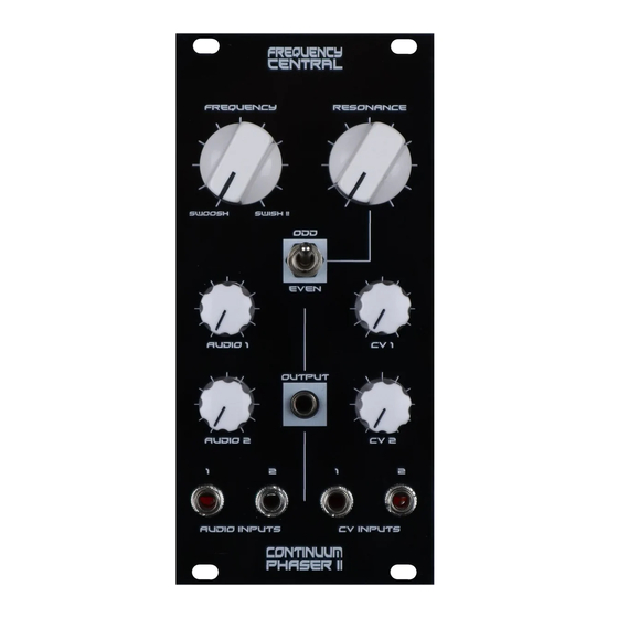
continuum phaser ii
An original design by
Frequency central
Rev 3 / May 2014
Main PCB:
Panel PCB:
Key to PCB screen print:
n: This signifies NPN BC547 transistors. Note the correct pinout as shown by the half circles.
p: This signifies PNP BC557 transistors. Note the correct pinout as shown by the half circles.
Please observe that the TL084 is 'the other way round' with respect to the LF351 and 2 x
LM13700.
Please observe the correct polarity of the 2 diodes and 8 electrolytic capacitors. The 6 x
22uF are configured in sets of 2 back to back (negative to negative).
Advertisement

Related Manuals for Frequency Central Continuum Phaser ii


Summary of Contents for Frequency Central Continuum Phaser ii
- Page 1 Build documentation for: continuum phaser ii An original design by Frequency central Rev 3 / May 2014 Main PCB: Panel PCB: Key to PCB screen print: n: This signifies NPN BC547 transistors. Note the correct pinout as shown by the half circles.
- Page 2 The PCB shows the correct orientation for BC547/BC557. Other transistor types can be used (eg 2N3904/2N3906), but please observe the correct pinout. Bill of materials 100R x 1 4n7 x 1 LF351 x 1 (or TL071) A100K x 3 1K5 x 1 10n x 4 LM13700 x 2 B100K x 3...
- Page 3 Now, place the 5 sockets onto the PCB with their ground lugs pointing towards the bottom of the PCB. Don’t solder them in place yet! Assemble the panel to the panel PCB, put on the pots/switch washers and tighten up the nuts. Now set the sockets to the panel using the nuts, making sure they all sit right.
Need help?
Do you have a question about the Continuum Phaser ii and is the answer not in the manual?
Questions and answers