
Related Manuals for Quectel MC60


Summary of Contents for Quectel MC60
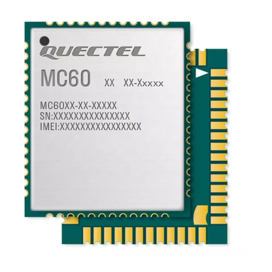
- Page 1 MC60 Reference Design GSM/GPRS/GNSS Module Series Rev. A Date: 2016-05-30 www.quectel.com...
-
Page 2: General Notes
QUECTEL OFFERS THE INFORMATION AS A SERVICE TO ITS CUSTOMERS. THE INFORMATION PROVIDED IS BASED UPON CUSTOMERS’ REQUIREMENTS. QUECTEL MAKES EVERY EFFORT TO ENSURE THE QUALITY OF THE INFORMATION IT MAKES AVAILABLE. QUECTEL DOES NOT MAKE ANY WARRANTY AS TO THE INFORMATION CONTAINED HEREIN, AND DOES NOT ACCEPT ANY LIABILITY FOR ANY INJURY, LOSS OR DAMAGE OF ANY KIND INCURRED BY USE OF OR RELIANCE UPON THE INFORMATION. -
Page 3: About The Document
GSM/GPRS/GNSS Module Series MC60 Reference Design About the Document History Revision Date Author Description 2016-05-30 Tiger CHENG Initial MC60_Reference_Design Confidential / Released 2 / 4... - Page 4 GSM/GPRS/GNSS Module Series MC60 Reference Design Contents About the Document ........................... 2 Contents ............................... 3 Introduction ............................4 1.1. Introduction ..........................4 1.2. Schematics ..........................4 MC60_Reference_Design Confidential / Released 3 / 4...
- Page 5 GNSS Module Series MC60 Reference Design Introduction 1.1. Introduction This document is a reference design for MC60 module. The schematics included in this document are preliminary and are subject to change without prior notice. 1.2. Schematics MC60_Reference_Design Confidential / Released...
-
Page 6: Module Design
RESERVED PCM_SYNC PCM_IN MC60 MC60 VCC_3V3 Reference Circuit of ADC NOTE VOLTAGE_INPUT R104 MC60 module does not support PCM / BT/SD card function R107 C115 R106 [1] GNSS_TXD RXD_AUX 100nF R108 TXD_AUX GNSS_RXD The voltage range of ADC input channel is from 0 to 2.8V. -
Page 7: Power Supply
4V & 3.3V typical voltage for the module. DC 4V OUT FOR DC 3.3V OUT FOR eg. DC12V IN DC 5V OUT DCDC GSM PART GNSS PART Quectel Wireless Solutions PROJECT TITLE DRAWN BY Tiger CHENG MC60 Reference Design SIZE... -
Page 8: Audio Design
C327 C328 C329 C330 10pF 33pF 33pF 10pF 10pF 33pF SPKN AGND Close to Socket Close to Socket Close to handset connector Quectel Wireless Solutions PROJECT TITLE DRAWN BY Tiger CHENG MC60 Reference Design SIZE CHECKED BY SHEET DATE 2016/5/30... - Page 9 2. U401 and U402 is used for protecting SIM card against ESD, and the junction capacitance should be less than 50pF. It should be placed nearby SIM card holder. 3. For MC60 module, ground of SIM card is recommended to be routed to the Pin 16("SIM_GND") of the module separately. Quectel Wireless Solutions...
- Page 10 Recommended circuit for turning on/off the module. LED Indication MCU GPIO VBAT D501 R501 GPIO PWRKEY_CONTROL POWER_ON/OFF GPIO GPIO Q503 NETLIGHT DTC143ZETL Pin "NETLIGHT" indicates the network status. Quectel Wireless Solutions PROJECT TITLE DRAWN BY Tiger CHENG MC60 Reference Design SIZE CHECKED BY SHEET DATE 2016/5/30...
-
Page 11: Serial Interface
4. DCD is mainly applied in modem communication (PPP). The active status represents the communication link has been set up. 5. Please pay attention to the level match of UART in product application. MC60 DBG_RXD T607 Quectel Wireless Solutions DBG_TXD T608 PROJECT TITLE DRAWN BY...
Need help?
Do you have a question about the MC60 and is the answer not in the manual?
Questions and answers