
Related Manuals for Quectel Mini PCIe-C EVB


Summary of Contents for Quectel Mini PCIe-C EVB
- Page 1 Mini PCIe-C EVB User Guide UMTS/HSPA+/LTE Standard Module Series Rev: Mini_PCIe-C_EVB_User_Guide_V1.0 Date: 2019-11-08 Status: Released www.quectel.com...
- Page 2 QUECTEL OFFERS THE INFORMATION AS A SERVICE TO ITS CUSTOMERS. THE INFORMATION PROVIDED IS BASED UPON CUSTOMERS’ REQUIREMENTS. QUECTEL MAKES EVERY EFFORT TO ENSURE THE QUALITY OF THE INFORMATION IT MAKES AVAILABLE. QUECTEL DOES NOT MAKE ANY WARRANTY AS TO THE INFORMATION CONTAINED HEREIN, AND DOES NOT ACCEPT ANY LIABILITY FOR ANY INJURY, LOSS OR DAMAGE OF ANY KIND INCURRED BY USE OF OR RELIANCE UPON THE INFORMATION.
-
Page 3: About The Document
UMTS/HSPA+/LTE Standard Module Series Mini PCIe-C EVB User Guide About the Document History Revision Date Author Description Jouni YANG/ 2019-11-08 Initial Woody WU Mini_PCIe-C_EVB_User_Guide 2 / 39... -
Page 4: Table Of Contents
Safety Information ........................7 General Overview ..........................8 2.1. Key Features ........................... 8 2.2. Component Placement of Mini PCIe-C EVB ................9 2.3. Top and Bottom Views of EVB ....................12 2.4. EVB Kit Accessories ......................13 EVB and Accessories Assembly ...................... 15 EVB Interface Application ......................... - Page 5 UMTS/HSPA+/LTE Standard Module Series Mini PCIe-C EVB User Guide Table Index TABLE 1: KEY FEATURES OF MINI PCIE-C EVB ..................... 8 TABLE 2: COMPONENT FUNCTIONS OF MINI PCIE-C EVB ................. 10 TABLE 3: ACCESSORIES LIST ........................13 TABLE 4: PIN DEFINITION OF J302 ........................ 18 TABLE 5: PIN DEFINITION OF J401 ........................
- Page 6 FIGURE 4: EVB BOTTOM VIEW ........................12 FIGURE 5: EVB KIT ACCESSORIES ....................... 13 FIGURE 6: MINI PCIE-C EVB AND ACCESSORIES ASSEMBLY..............15 FIGURE 7: EVB POWER SUPPLY BLOCK DIAGRAM ..................16 FIGURE 8: EVB POWER SUPPLY INTERFACE ....................17 FIGURE 9: POWER PLUG DESIGN .........................
-
Page 7: Introduction
This document describes how to use the evaluation board of Mini PCIe-C modules. It is an assistant tool to develop and test Quectel Mini PCIe-C/-D and EP200F modules. 1.1. Applicable Modules Mini PCIe-C EVB is applicable to the following modules. Please refer to document [1], [2] or [3] for more details about these modules. ... -
Page 8: Safety Information
If not so, Quectel assumes no liability for customers’ failure to comply with these precautions. -
Page 9: General Overview
UMTS/HSPA+/LTE Standard Module Series Mini PCIe-C EVB User Guide General Overview Quectel supplies the Mini PCIe-C EVB to facilitate application design based on Quectel Mini PCIe-C/-D and EP200F modules. It can test module basic functionalities. 2.1. Key Features The following table describes the detailed features of Mini PCIe-C EVB. -
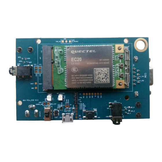
Page 10: Component Placement Of Mini Pcie-C Evb
UMTS/HSPA+/LTE Standard Module Series Mini PCIe-C EVB User Guide 2.2. Component Placement of Mini PCIe-C EVB (U)SIM card connector VDD_EVT J104 J103 J303 WAKEUP_IN W_DISABLE WAKEUP_OUT J402 J301 J403 J101 J102 Mini PCIe Card VDD_3V3 VBAT Status LEDs D103 D101... - Page 11 J303 J301 J503 J201 Power Audio interfaces supply Figure 2: Component Placement of EVB Bottom Side (Unit: mm) Table 2: Component Functions of Mini PCIe-C EVB Component Functions Description J201 The power jack on the EVB Power Supply ...
- Page 12 UMTS/HSPA+/LTE Standard Module Series Mini PCIe-C EVB User Guide Used to test the analog audio function of Mini PCIe-C and EP200F modules J303 (U)SIM USIM/SIM card connector (bottom side) J301 UART port (bottom side) D101 is used to indicate the network status of Mini PCIe-C/...
-
Page 13: Top And Bottom Views Of Evb
UMTS/HSPA+/LTE Standard Module Series Mini PCIe-C EVB User Guide 2.3. Top and Bottom Views of EVB The top and bottom views of the Mini PCIe-C EVB are shown as below. Figure 3: EVB Top View Figure 4: EVB Bottom View... -
Page 14: Evb Kit Accessories
UMTS/HSPA+/LTE Standard Module Series Mini PCIe-C EVB User Guide 2.4. EVB Kit Accessories All accessories of the EVB kit are listed below. Instruction Sheet RS-232 Converter Cable Main Antennas Disk USB Flash Disk RF Cables USB Cable Earphone GNSS Antennas... - Page 15 UMTS/HSPA+/LTE Standard Module Series Mini PCIe-C EVB User Guide GNSS antenna (passive) Audio Earphone Disk USB 2.0 to RS-232 driver Including Mini PCIe module’s related USB Flash Disk documents, tools, drivers, etc. Others Bolts and nuts for assembling EVB 4 for each type...
-
Page 16: Evb And Accessories Assembly
UMTS/HSPA+/LTE Standard Module Series Mini PCIe-C EVB User Guide EVB and Accessories Assembly The following figure shows the assembly of Mini PCIe EVB and its accessories. Figure 6: Mini PCIe-C EVB and Accessories Assembly Mini_PCIe-C_EVB_User_Guide 15 / 39... -
Page 17: Evb Interface Application
4.1. Power Supply (J201/J302) The Mini PCIe-C EVB can be powered by an external power adapter through connecting with the power jack (J201) or USB connector (J302) on the EVB. The power adapter is designed to be connected to a step-down converter (U201), which can convert the supplied voltage into proper voltage (VBAT) for the Mini PCIe-C/-D and EP200F modules. -
Page 18: Usb Interface (J302)
GNSS NMEA output. The Mini PCIe-C EVB provides a micro-USB interface J302 for connection with a host device. The USB data lines USB_DP and USB_DM are connected directly to the Mini PCIe-C/-D or EP200F module. The USB_VBUS line can be used for USB connection detection and EVB power supply. -
Page 19: Audio Interfaces
The Mini PCIe-C EVB provides four audio interfaces J401, J404, J402 and J403. J401 and J404 are used to test the PCM function of Mini PCIe-C or EP200F module by connecting to codec TLV320AIC1106, and J402 and J403 are used to test the analog audio function of Mini PCIe-C and EP200F modules. -
Page 20: Earphone Interface (J401)
UMTS/HSPA+/LTE Standard Module Series Mini PCIe-C EVB User Guide TLV320AIC1106 TXS0104E AVDD_3.0V PCM_CLK MCLK PCM_SYNC PCMSYNC MIC_P (J401/J404) PCM_IN PCMO MIC_N PCM_OUT PCMI VDDA VDDB VDD_1.8V VDD_3.0V SPK_P U402 Handset (J401/J404) SPK_N J101 U401 Figure 11: Reference Circuit Design for Codec ... - Page 21 UMTS/HSPA+/LTE Standard Module Series Mini PCIe-C EVB User Guide The figure and table below illustrate the pin assignment and pin definition of the earphone interface J401. Figure 13: Pin Assignments of Earphone Interface J401 Table 5: Pin Definition of J401 Pin No.
-
Page 22: Handset Interface (J404)
UMTS/HSPA+/LTE Standard Module Series Mini PCIe-C EVB User Guide 4.3.1.2. Handset Interface (J404) The analog audio interface J404 is designed for handset. Its reference circuit design is shown as below. CODEC 10pF 33pF 10pF 33pF 10pF 33pF MIC_P MIC_N SPK_P... -
Page 23: Analog Audio Interfaces (J402/J403)
UMTS/HSPA+/LTE Standard Module Series Mini PCIe-C EVB User Guide Table 6: Pin Definition of J404 Pin No. Pin Name Function MICN Negative microphone input SPKN Negative speaker output SPKP Positive speaker output MICP Positive microphone input NOTE Software functions of J401 and J404 are not supported. - Page 24 UMTS/HSPA+/LTE Standard Module Series Mini PCIe-C EVB User Guide The figure and table below illustrate the pin assignment and pin definition of the handset interface J402. Figure 17: Pin Assignments of Handset Interface J402 Table 7: Pin Definition of J402 Pin No.
-
Page 25: Earphone Interface (J403)
UMTS/HSPA+/LTE Standard Module Series Mini PCIe-C EVB User Guide 4.3.2.2. Earphone Interface (J403) The analog audio interface J403 is designed for CTIA earphone. Its reference circuit design is shown as below. GND GND Differential 4.7uF layout 33pF 10pF MICN Audio Jack... -
Page 26: U)Sim Interface (J303)
32Ω Figure 20: Sketch Design of CTIA Audio Plug 4.4. (U)SIM Interface (J303) The Mini PCIe-C EVB provides a 6-pin push-push type (U)SIM interface J303 which supports 1.8V/3.0V (U)SIM card. Its reference circuit design is shown as below. Mini_PCIe-C_EVB_User_Guide 25 / 39... - Page 27 UMTS/HSPA+/LTE Standard Module Series Mini PCIe-C EVB User Guide Push-Push SIM_VDD SIM_VDD SIM_DATA SIM_DATA SIM_CLK SIM_CLK SIM_RST SIM_RST SIM_GND (U)SIM card connector J303 J101 Figure 21: Reference Circuit Design for (U)SIM Interface J303 The figure and table below illustrate the pin assignment and pin definition of the (U)SIM interface J303.
-
Page 28: Uart Interface (J301)
Not connected 4.5. UART Interface (J301) The UART interface of the Mini PCIe-C EVB is intended for the communication between the module and the host application. It can be used for data transmission and AT command communication. The following figure shows the block diagram of the UART interface on Mini PCIe-C EVB. - Page 29 UMTS/HSPA+/LTE Standard Module Series Mini PCIe-C EVB User Guide The figure and table below illustrate the pin assignment and pin definition of UART interface J301. Figure 24: Pin Assignments of UART Interface J301 Table 10: Pin Definition of J301 Pin No.
-
Page 30: Switch And Button (S201/S101)
UMTS/HSPA+/LTE Standard Module Series Mini PCIe-C EVB User Guide 4.6. Switch and Button (S201/S101) Mini PCIe-C EVB provides a switch S201 and a button S101, which are shown as the following figure. S101 S201 Figure 25: Switch S201 and Button S101 Table 11: Description of S201 and S101 Reference No. -
Page 31: Status Indicators (D103/D101)
UMTS/HSPA+/LTE Standard Module Series Mini PCIe-C EVB User Guide 4.7. Status Indicators (D103/D101) The Mini PCIe-C EVB provides two status indicators D103 and D101. The following figure shows the location of the two LED indicators. D103 D101 Figure 26: Status Indicators Table 12: Description of D103 and D101 Reference No. -
Page 32: Test Points
Mini PCIe-C EVB User Guide 4.8. Test Points The Mini PCIe-C EVB provides a series of test points, which can facilitate to obtain the corresponding waveform of some signals. The following figure shows the test points. Figure 27: Test Points... - Page 33 UMTS/HSPA+/LTE Standard Module Series Mini PCIe-C EVB User Guide Connected directly to PCM’s PCM_OUT of Mini PCIe-C or EP200F module PCM_OUT Connected directly to PCM’s PCM_IN of Mini PCIe-C or EP200F module PCM_IN Connected directly to USB’s USB_DM of Mini PCIe-C/-D or EP200F module Connected directly to USB’s USB_DP of Mini PCIe-C/-D or EP200F module...
-
Page 34: Operation Procedures Illustration
UMTS/HSPA+/LTE Standard Module Series Mini PCIe-C EVB User Guide Operation Procedures Illustration This chapter introduces how to use the Mini PCIe-C EVB for testing and evaluation of Quectel Mini PCIe-C/-D modules. 5.1. Turn on the Mini PCIe-C/-D and EP200F Modules 1. -
Page 35: Communication Via Uart Interface
Figure 29: USB Ports for EC200T Mini PCIe-C/EC200T-CN Mini PCIe-D Install and then use the QCOM tool provided by Quectel to realize the communication between the EVB and the PC. The following figure shows the COM Port Setting field on QCOM: select correct “COM port”... -
Page 36: Firmware Upgrade
UMTS/HSPA+/LTE Standard Module Series Mini PCIe-C EVB User Guide 5.3. Firmware Upgrade Quectel Mini PCIe-C module upgrades firmware via USB port by default. Please follow the procedures below to upgrade firmware. 5.3.1. Firmware Upgrade (UC20/EC20 R2.0/EC20 R2.1 Mini PCIe-C/EP200F) Install and open the firmware upgrade tool QFlash on PC and then power on the module according to the procedures mentioned in Chapter 5.1. -
Page 37: Reset The Mini Pcie-C/-D And Ep200F Modules
UMTS/HSPA+/LTE Standard Module Series Mini PCIe-C EVB User Guide Figure 34: Firmware Upgrade (EC200T Mini PCIe-C/EC200T-CN Mini PCIe-D) 5.4. Reset the Mini PCIe-C/-D and EP200F Modules The reset option is only used in case of emergency. For example, the software does not respond for more than 5s due to some serious problems. -
Page 38: Turn Off The Mini Pcie-C/-D And Ep200F Modules
UMTS/HSPA+/LTE Standard Module Series Mini PCIe-C EVB User Guide 5.5. Turn off the Mini PCIe-C/-D and EP200F Modules There are two ways to turn off the Mini PCIe-C/-D and EP200F modules. Execute AT+QPOWD via PC. This is the best and the safest way. The module will log off from the network and save data before the shutdown, but it will be turned on again after shutdown. -
Page 39: Appendix A References
UMTS/HSPA+/LTE Standard Module Series Mini PCIe-C EVB User Guide Appendix A References Table 14: Related Documents Document Name Remark Hardware design for UC20, EC20 R2.0, Quectel_XX_Mini_PCIe-C_Hardware_Design EC20 R2.1, EC200T Mini PCIe-C modules Quectel_EC200T_Mini_PCIe-D_Hardware_Design EC200T Mini PCIe-D hardware design Quectel_EP200F_Hardware_Design EP200F hardware design... - Page 40 UMTS/HSPA+/LTE Standard Module Series Mini PCIe-C EVB User Guide Input/Output Light Emitting Diode Microphone Not Connected Pulse-code Modulation Power Output Radio Frequency UART Universal Asynchronous Receiver & Transmitter (U)SIM (Universal) Mobile Telecommunication System VBAT Voltage of Battery Mini_PCIe-C_EVB_User_Guide 39 / 39...
Need help?
Do you have a question about the Mini PCIe-C EVB and is the answer not in the manual?
Questions and answers