Table of Contents
Advertisement
Quick Links
Advertisement
Table of Contents

Related Manuals for Quectel M20


Summary of Contents for Quectel M20
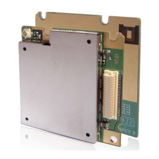
- Page 1 Quectel Cellular Engine Hardware Design M20_HD_V1.01...
- Page 2 Document Control ID General Notes Quectel offers this information as a service to its customers, to support application and engineering efforts that use the products designed by Quectel. The information provided is based upon requirements specifically provided to Quectel by the customers. Quectel has not undertaken any independent search for additional relevant information, including any information that may be in the customer’s possession.
-
Page 3: Table Of Contents
M20 Hardware Design Contents 0 Revision history ..........................8 1 Introduction............................9 1.1 Related documents .......................9 1.2 Terms and abbreviations.....................10 1.3 Safety caution........................12 2 Product concept..........................14 2.1 Key features ........................14 2.2 Functional diagram......................16 2.3 Evaluation board ........................17 3 Application interface........................18 3.1 Pin description........................18 3.2 Operating modes ........................22... - Page 4 7.3.3 Physical photo of the DF12 connector ..............75 7.4 RF connector ........................76 7.4.1 Physical photo of the UF.L-R-SMT connector............76 7.4.2 Matching connector on the application side of M20 ..........76 7.4.3 Space factor of mated connector ................77 7.5 Top view of the module .....................78 7.6 Bottom view of the module ....................78...
- Page 5 M20 Hardware Design Table Index TABLE 1: RELATED DOCUMENTS.....................9 TABLE 2: TERMS AND ABBREVIATIONS ..................10 TABLE 3: MODULE KEY FEATURES....................14 TABLE 4: CODING SCHEMES AND MAXIMUM NET DATA RATES OVER AIR INTERFACE..16 TABLE 5: PIN DESCRIPTION ......................18 TABLE 6: OVERVIEW OF OPERATING MODES................22 TABLE 7: RECOMMENDED BYPASS CAPACITORS FOR LIMITED CURRENT SUPPLY..25...
- Page 6 M20 Hardware Design TABLE 41: GPRS MULTI-SLOT CLASSES ..................80 M20_HD_V1.01 - 5 -...
- Page 7 M20 Hardware Design Figure Index FIGURE 1: MODULE FUNCTIONAL DIAGRAM ................17 FIGURE 2: REFERENCE BYPASS CAPACITORS FOR THE VBAT INPUT........24 FIGURE 3: REFERENCE CIRCUIT OF THE SOURCE POWER SUPPLY INPUT......24 FIGURE 4: RIPPLE IN SUPPLY VOLTAGE DURING TRANSMITTING BURST ......25 FIGURE 5: TURN ON THE MODULE BY USING DRIVING CIRCUIT ..........27...
- Page 8 FIGURE 42: ANTENNA PAD AND RF CONNECTOR...............62 FIGURE 43: M20 TOP AND SIDE DIMENSIONS(UNIT: MM)............72 FIGURE 44: M20 MODULE MATCHS WITH THE APPLICATION BOARD(UNIT: MM) ..72 FIGURE 45: FOOTPRINT OF RECOMMENDATION(UNIT: MM)..........73 FIGURE 46: DIMENSIONS OF THE DF12 HEADER(UNIT: MM)..........74 FIGURE 47: FOOTPRINT OF RECOMMENDATION(UNIT: MM)..........75...
-
Page 9: Revision History
M20 Hardware Design 0 Revision history Revision Date Author Description of change 1.00 2009-09-8 Yong AN Initial 1.01 2009-09-17 Yong AN Add SIM_GND Pin name descriptions Modify Figure 33 and Figure 34 about SIM card circuit Add current consumption of 2 Rx and 3 Tx in data mode Modify ordering information content in Chapter 6 M20_HD_V1.01... -
Page 10: Introduction
This document defines and specifies the M20 module series. For product ordering information, please refer to Chapter 6 Product Information.This document describes the hardware interface of Quectel’s M20 module series that connects to the specific application and the air interface. This document can help you quickly understand module interface specifications, electrical and mechanical details. -
Page 11: Terms And Abbreviations
M20 Hardware Design 1.2 Terms and abbreviations Table 2: Terms and abbreviations Abbreviation Description Analog-to-Digital Converter Adaptive Multi-Rate Antenna Reference Point ASIC Application Specific Integrated Circuit Bit Error Rate Board-to-Board Base Transceiver Station CHAP Challenge Handshake Authentication Protocol Coding Scheme... - Page 12 M20 Hardware Design Li-Ion Lithium-Ion Mobile Originated Mobile Station (GSM engine), also Referred to as TE Mobile Terminated Password Authentication Protocol PBCCH Packet Switched Broadcast Control Channel Printed Circuit Board Protocol Data Unit Point-to-Point Protocol Radio Frequency Root Mean Square (value)
-
Page 13: Safety Caution
The following safety precautions must be observed during all phases of the operation. Usage , service or repair of any cellular terminal or mobile incorporating M20 module. Manufactures of the cellular terminal should send words the following safety information to users and operating personnel and to incorporate these guidelines into all manuals supplied with the product. - Page 14 M20 Hardware Design GSM cellular terminals or mobiles operate over radio frequency signals and cellular networks and cannot be guaranteed to connect in all conditions, for example no mobile fee or a invalid SIM card. While you are in this condition and need emergent help, Please Remember using emergency calls.
-
Page 15: Product Concept
The M20 is a Quad-band GSM/GPRS engine that works at frequencies GSM850, EGSM 900 MHz, DCS 1800 MHz and PCS 1900 MHz. The M20 features GPRS multi-slot class 12(default)/ class 10/class8 and supports the GPRS coding schemes CS-1, CS-2, CS-3 and CS-4. For more detail about GPRS multi-slot classes and coding schemes, please refer to Appendix A and Appendix B. - Page 16 M20 Hardware Design Class 1 (1W) at DCS 1800 and PCS 1900 GPRS connectivity GPRS multi-slot class 12 (default) GPRS multi-slot class 10 (option) GPRS multi-slot class 8 (option) GPRS mobile station Class B Temperature range Normal operation: -35°C ~ +80°C Restricted operation: -45°C ~ -35°C and +80°C ~ +85°C ○...
-
Page 17: Functional Diagram
62.4kbps CS-4: 21.4kbps 42.8kbps 85.6kbps 2.2 Functional diagram The following figure shows a block diagram of the M20 module and illustrates the major functional part: The GSM baseband engine Flash and SRAM The GSM radio frequency part The antenna interface The B2B interface —SIM card interface... -
Page 18: Evaluation Board
Figure 1 : Module functional diagram 2.3 Evaluation board In order to help customer on the application of M20, Quectel can supply an Evaluation Board (EVB) that hosts the module directly with appropriate power supply, SIM card holder, RS-232 serial interface, handset RJ11 port, earphone port, antenna and other peripherals to control or test the module. -
Page 19: Application Interface
M20 Hardware Design 3 Application interface The module is equipped with a 50-pin 0.5mm pitch B2B connector that connects to the cellular application platform. Sub-interfaces included on this B2B connector are described in details in the following chapters: Power supply (refer to Chapter 3.3) Serial interface (refer to Chapter 3.9) - Page 20 M20 Hardware Design VDD_EXT Supply 2.8V voltage for Vmax=2.9V 1.If unused, external circuit. Vmin=2.7V keep this pin measuring this pin, customer Vnorm=2.8V open. judge whether Imax=20mA system is power on or off. Recommend When the voltage is low, the system power off.
- Page 21 M20 Hardware Design MIC2P Audio input channel Microphone MIC2N Positive and negative voice bias voltage input. supplied internally. unused, keep these pins open. SPK1P Audio output channel 1. unused SPK1N Positive and negative voice keep these output. pins open. SPK2P Audio output channel 2.
- Page 22 M20 Hardware Design VOLmax=0.34V connect RTS0 Ring indicator VOHmin=2.0V pin to GND DCD0 Data carrier detection VOHmax= VDD_EXT directly. If unused keep these pins open. Serial Port 1 RXD1 Receiving data If unused keep these pins TXD1 Transmitting data open.
-
Page 23: Operating Modes
M20 Hardware Design from low to high, module would execute a SIM card initialization process. unused keep this pin open. SIM_GND Digital Ground of SIM Card This internally connected dedicated for Card ground. AUXADC PIN NAME DESCRIPTION DC CHARACTERISTICS COMMENT... -
Page 24: Power Supply
A lower cost choice could be a 100 µF tantalum capacitor with low ESR. A small (0.1µF to 1µF) ceramic capacitor should be in parallel with the 100µF capacitor, which is illustrated in Figure 2. The capacitors should be placed as close as possible to the M20 VBAT pins. - Page 25 M20 Hardware Design VBAT C1=100µF, C2=0.1µF~1µF Figure 2 : Reference bypass capacitors for the VBAT input The circuit design of the power supply for the module largely depends on the power source. Figure 3 shows a reference design of +5V input power source. The designed output for the power supply is 4.16V, thus a linear regulator can be used.
-
Page 26: Power Supply Pins
M20 Hardware Design Table 7: Recommended bypass capacitors for limited current supply Maximum Capacitance ESR@ Part number Quantity of Vendor current +25°C application output of 100KHz power (Ω) supply 1.5A 1500µF <=0.045 VISHAY 592D158X06R3R2T20H 2200µF <=0.055 VISHAY 592D228X06R3X2T20H The single 3.6V Li-Ion cell battery type can be connected to the power supply of the module VBAT directly. -
Page 27: Monitoring Power Supply
M20 Hardware Design current consumption may rise up to 1.6A. If the power voltage drops below 3.4V, the module may be switched off. The PCB traces from the VBAT pads to the power source must be wide enough to ensure that there isn’t too much voltage drop occur in the transmitting burst mode. - Page 28 M20 Hardware Design PWRKEY 4.7K Turn on impulse Figure 5: Turn on the module by using driving circuit The other way to control the PWRKEY is using a button directly. A TVS component is indispensable to be placed nearby the button for ESD protection. When pressing the key, electrostatic strike may generate from finger.
- Page 29 M20 Hardware Design VBAT Pulldown > 2s PWRKEY > 0.6*VBAT (INPUT) <0.2*VBAT VDD_EXT (OUTPUT) Figure 7: Timing of turn on the module When the power-on procedure completes, the module will send out the following result code to indicate the module is ready to operate when the baud rate of the serial port is set to fixed.
-
Page 30: Turn Off
M20 Hardware Design will return 0 which indicates that the protocol stack is closed. After 90 seconds, the module will power down automatically. However, if the GSM protocol stack is started by “AT+CFUN=1” command during the alarm mode, the process of automatic power-off will not be executed. In alarm mode, driving the PWRKEY to a low level voltage for a period will cause the module to power down (Please refer to the power down chapter). - Page 31 M20 Hardware Design Logout net about 2s to 8s 1s > Pulldown > 0.6s PWRKEY (INPUT) >0.7*VBAT <0.3*VBAT VDD_EXT (OUTPUT) Figure 8: Timing of turn off the module 3.4.2.2 Turn off module using AT command Customer’s application can use an AT command “AT+QPOWD=1” to turn off the module. This command will let the module to log off from the network and allow the software to save important data before completely disconnecting the power supply, thus it is a safe way.
- Page 32 M20 Hardware Design If the voltage ≤ 3.4V, the following URC will be presented: UNDER-VOLTAGE POWER DOWN If the voltage ≥ 4.6V, the following URC will be presented: OVER-VOLTAGE POWER DOWN After this moment, no further AT command can be executed. The module logoff from network and enters POWER DOWN mode, and only RTC is still active.
-
Page 33: Restart Module Using The Pwrkey Pin
M20 Hardware Design shutdown the system. Although turning off the module by EMERG_OFF is fully tested and nothing wrong detected, this operation is still a big risk as it could cause destroying of the code or data area of the NOR flash memory in the module. Therefore, it is recommended that PWRKEY or AT command should always be the preferential way to turn off the system. -
Page 34: Charging Interface
Battery pack Figure 13: Charging circuit connection The charging function is not supported in standard M20 module. If customer needs this function, it would be necessary to contact Quectel. Furthermore, when battery charging is done by the charging function supported by the module, the VBAT would be mainly supplied by the battery and the external power source is used to charging the battery. -
Page 35: Battery Pack Characteristics
M20 Hardware Design DC5V/2A Module 4.3V~4.4V ACIN VOUT VBAT 100uF 220uF 100nF 100nF PMOS 100K Charge IC ACIN VBAT Batttery Pack 10uF Figure 14: Reference external battery charging circuit Figure 14 shows the reference battery charging circuit for M2M application. U1 is an LDO which can supply current more than 2A and can output a voltage of 4.3~4.4V through adjusting the... -
Page 36: Recommended Battery Pack
M20 Hardware Design characteristics listed below. To use the module’s charging algorithm properly, it is recommended that the battery pack is compliant with these specifications, as it is important for the AT command “AT+CBC” to monitor the voltage of battery properly, or the “AT+CBC” may return incorrect battery capacity value. -
Page 37: Implemented Charging Technique
M20 Hardware Design Charging Voltage 4.200~4.23V Max Charging Current 1.2C Max Discharge Current Charging Method CC / CV (Constant Current / Constant Voltage) Internal resistance ≤130mΩ Over-charge protect threshold.(V) 4.28 ± 0.025 Released Voltage from Over-charge(V) 4.08 ± 0.05 Over-discharge protect threshold(V) 2.3±... - Page 38 M20 Hardware Design DDLO charging terminates when the battery voltage reaches 2.4V. UVLO charging terminates when the battery voltage is up to 3.2V. Both DDLO and UVLO charging are controlled by the module hardware only. CC charging: When an external charger supply and battery have been inserted and the battery voltage is higher than 3.2V, the module enters CC charging stage.
-
Page 39: Operating Modes During Charging
M20 Hardware Design The charging process is shown in Figure 15. Figure 15: Normal charging process diagram 3.5.4 Operating modes during charging The battery can be charged in various working modes such as SLEEP, TALK and GPRS DATA. It is named as Charging mode. -
Page 40: Charger Requirements
M20 Hardware Design Table 11: Operating modes How to activate Features Connect charger to module’s VCHG pin, The module can normally operate. connect battery to VBAT pin of module while the module is in Normal operating mode, including: IDLE, TALK, GPRS STANDBY, GPRS READY and GPRS DATA mode, etc. -
Page 41: Power Saving
M20 Hardware Design A 1.6A peak current is allowed for maximum 1ms when charging current is switched on. 3.6 Power saving There are two methods to drive the module enter low current consumption status. “AT+CFUN” is used to set module into minimum functionality mode and DTR hardware interface signal can be used to lead system to enter SLEEP mode. -
Page 42: Wake Up Module From The Sleep Mode
M20 Hardware Design 3.6.3 Wake up module from the SLEEP mode When the module is in the SLEEP mode, the following methods can wake up the module. DTR pin If the DTR Pin is pulled down to a low level, it would wake up the module from SLEEP mode. - Page 43 M20 Hardware Design Module 3.9K VRTC Core Non-chargeable Backup Battery Figure 16: RTC supply from non-chargeable battery Module 3.9K VRTC Core Rechargeable Backup Battery Figure 17: RTC supply from rechargeable battery Module 3.9K VRTC Core Large-capacitance Capacitor Figure 18: RTC supply from capacitor Coin-type rechargeable capacitor such as XH414H-IV01E form Seiko can be used.
-
Page 44: Serial Interface
M20 Hardware Design Figure 19 : Seiko XH414H-IV01E charging characteristic 3.9 Serial interface The module provides two unbalanced asynchronous serial ports, serial port0 and serial port1. The module is designed as a DCE (Data Communication Equipment), following the traditional DCE-DTE (Data Terminal Equipment) connection. The module and DTE are connected through the following signal in Figure 20. - Page 45 M20 Hardware Design Module (DCE) CUSTOMER (DTE) Serial port0 Serial port1 TXD0 RXD0 RTS0 CTS0 DTR0 DCD0 RING Serial port1 Serial port2 TXD1 /TXD RXD1 /RXD Figure 20 : Connection of serial interfaces Serial Port 0 TXD0: Send data to the RXD signal line of DTE RXD0: Receive data from the TXD signal line of DTE When hardware flow control is required, RTS0 and CTS0 should also be connected.
-
Page 46: Function Of Serial Port 0 & Serial Port 1
M20 Hardware Design Table 14: Logic levels of serial port Parameter Unit 0.67 1.67 VDD_EXT +0.3 0.34 VDD_EXT Table 15: Pin definition of serial interface Interface Name Function Ring indicator RTS0 Request to send CTS0 Clear to send Serial port 0... -
Page 47: Software Upgrade And Software Debug
M20 Hardware Design Synchronization between DTE and DCE: When DCE (the module) powers on with the autobauding enabled, it is recommended to wait for 2 to 3 seconds before sending the first AT character. After receiving the “OK” response, DTE and DCE are correctly synchronized. - Page 48 M20 Hardware Design Module(DCE) CUSTOMER(DTE) Serial port1 TXD1 RXD1 Figure 22: Connection of software debugging The serial port 0 and the serial port 1 don’t support the RS-232 level, but only support the CMOS level. A level shifter IC or circuit may be inserted between DCE and DTE. Figure 23 shows a reference level shifter circuit when the module is connected to a PC.
-
Page 49: Audio Interfaces
M20 Hardware Design 3.10 Audio interfaces The module provides two audio input channels and two audio output channels and one serial digital audio interface (DAI) on the B2B connector. AIN1 and AIN2, which may be used for both microphone and line inputs.An electret microphone is usually used. -
Page 50: Microphone Interface Configuration
M20 Hardware Design 3.10.1 Microphone interface configuration AIN1 channel has no internal bias supply for external microphone, thus an external bias circuit must be added when connecting electret microphone to AIN1 channel. A reference circuit is shown in Figure 24. The LDO to supply VMIC should use AGND of the module as its ground instead of GND of the module to suppress TDD noise. - Page 51 M20 Hardware Design Close to Microphone Differential layout 10pF 33pF ANTI MIC2P 10pF 33pF Module MIC2N Electret Microphone 33pF 10pF ANTI AGND Figure 25: Electret microphone interface configuration of AIN2 If AIN1/AIN2 channels are connected to other type of audio signal source instead of electret microphone, for example, an op amp or a moving-coil type microphone, it is recommended to insert two 10μF capacitors for decoupling.
-
Page 52: Speaker Interface Configuration
M20 Hardware Design 3.10.2 Speaker interface configuration Close to speaker Differential layout 10pF 33pF ANTI SPK1P Moudule 10pF 33pF SPK1N 10pF 33pF ANTI Figure 27: Speaker interface configuration of AOUT1 Close to speaker Differential layout Amplifier 10pF 33pF circuit ANTI... - Page 53 M20 Hardware Design Close to speaker Differential layout 33pF 10pF ANTI SPK2P Module AGND Figure 29: Speaker interface configuration of AOUT2 Close to speaker Differential layout Amplifier 10pF 33pF circuit ANTI SPK2P Module AGND 10pF 33pF ANTI Figure 30: Speaker interface with amplifier in AOUT2 Note: The value of C1 and C2 depends on the input impedance of audio amplifier .
-
Page 54: Earphone Interface Configuration
Note: The module supports optionally earphone detection and hook off in hardware, In other words, it is not supported in default hardware configuration. If customer needs earphone detection or hook off detection, please contact Quectel. Table 17: Typical electret microphone input characteristic... -
Page 55: Dai Interface(Optional
M20 Hardware Design Table 18: Typical speaker output characteristic Parameter Unit Normal Single load Ω Output(SPK1) Ended Resistance Ref level Differential load Ω Resistance Ref level Auxiliary Single load Ω Output(SPK2) Ended Resistance Ref level Maxim driving current limit of... -
Page 56: Sim Card Interface
M20 Hardware Design Figure 32: Timing diagram of DAI interface Note: This function is not supported in the default firmware. If need, please contact Quectel. 3.11 SIM card interface 3.11.1 SIM card application Customer can get information in SIM card by AT Command. For more information, please refer to document [1]. - Page 57 M20 Hardware Design Figure 33 is the reference circuit for SIM interface, and here an 8-pin SIM card holder is used. In order to offer good ESD protection, it is recommended to add TVS such as ST (www.st.com ) ESDA6V1W5 or ON SEMI (www.onsemi.com ) SMF05C. The 22Ω resistors should be added in series between the module and the SIM card so as to suppress the EMI spurious transmission and enhance the ESD protection.
-
Page 58: Design Considerations For Sim Card Holder
M20 Hardware Design SIM CARD SIM_GND Module MOLEX-91228 SIM_VDD SIM_RST SIM_CLK SIM_PRESENCE SIM_DATA SMF05C Figure 34: Reference circuit of using 6-pin SIM card socket 3.11.2 Design considerations for SIM card holder For 6-pin SIM card holder, it is recommended to use Amphenol C707 10M006 512 2. Please visit http://www.amphenol.com for more information. - Page 59 M20 Hardware Design Table 21: Pin description (Amphenol SIM card holder) Name Function SIM_VDD SIM Card Power supply SIM_RST SIM Card Reset. SIM_CLK SIM Card Clock. Ground Not connect. SIM_DATA SIM Card data I/O. For 8-pin SIM card holder, it is recommended to use Molex 91228.Please visit http://www.molex.com for more information.
-
Page 60: Adc
M20 Hardware Design Not connect SIM_DATA SIM Card data I/O SIM_PRESENCE C8 SIM Card Presence detection 3.12 ADC The pin ADC1 can be used to measure analog voltage. Customer can get the measurement result through AT command “AT+QEADC”. Table 23: Pin definition of the ADC... - Page 61 M20 Hardware Design If the module is used as a caller, the RI0 would maintain high. On the other hand, when it is used as a receiver, the timing of the RI0 is shown below. HIGH Off-hook by “ATA”. On-hook by “ATH”.
-
Page 62: Network Status Indication
M20 Hardware Design HIGH 120ms URC or Idle or SMS Received talking Figure 40 : RI0 behaviour of URC or SMS received 3.14 Network status indication The NETLIGHT signal can be used to drive a network status indication LED. The working state of this pin is listed in Table 26. -
Page 63: Antenna Interface
M20 Hardware Design 4 Antenna interface The RF interface has an impedance of 50Ω. To suit the physical design of individual application M20 offers two alternatives: Recommended approach: antenna connector at the component side of the PCB (top view on M20). -
Page 64: Antenna Pad
M20 Hardware Design Table 27: Product specifications of U.FL-R-SMT Item Specification Condition Nominal 50Ω. Temperature: -40℃ to 90℃ impedance Frequency range DC to 6GHz. Contact Center: 20mΩ max. 10mA max. resistance Outer: 10mΩ max. Insulation 500 MΩ min. 100V DC... -
Page 65: Rf Output Power
M20 Hardware Design Note: The soldering time for antenna pad and GND pad are different, less than 5s for antenna pad and less than 10s for GND plan. 4.2 RF output power Table 28: The module conducted RF output power... -
Page 66: Electrical, Reliability And Radio Characteristics
M20 Hardware Design 5 Electrical, reliability and radio characteristics 5.1 PIN assignment of the module Table 31: PIN assignment PIN NO. PIN NAME PIN NO. PIN NAME SIM_CLK AGND SIM_VDD SPK2P SIM_DATA SPK1P SIM_RST SPK1N SIM_PRESENCE MIC2N SIM_GND MIC2P RXDDAI MIC1P TFSDAI MIC1N... -
Page 67: Absolute Maximum Ratings
M20 Hardware Design 5.2 Absolute maximum ratings The absolute maximum rating for power supply and voltage on digital and analog pins of module are listed in the following table: Table 32: Absolute maximum ratings Parameter Unit VBAT Peak current of power supply... -
Page 68: Current Consumption
M20 Hardware Design Voltage ripple Normal condition, power control level for Pout max @ f<200kHz @ f>200kHz Average supply POWER DOWN mode VBAT current SLEEP mode @ DRX=5 Minimum functionality mode AT+CFUN=0 IDLE mode SLEEP mode AT+CFUN=4 IDLE mode SLEEP mode... - Page 69 M20 Hardware Design Table 35: The module current consumption Condition Current Consumption Voice Call GSM850 @power level #5 <300mA,Typical 250mA @power level #12,Typical 130mA @power level #19,Typical 95mA EGSM 900 @power level #5 <300mA,Typical 240mA @power level #12,Typical 130mA @power level #19,Typical 95mA DCS 1800 @power level #0 <250mA,Typical 180mA...
- Page 70 M20 Hardware Design DATA mode, GPRS ( 2 Rx, 3 Tx ) CLASS 12 GSM850 @power level #5 <600mA,Typical 560mA @power level #12,Typical 240mA @power level #19,Typical 150mA EGSM 900 @power level #5 <600mA,Typical 530mA @power level #12,Typical 235mA @power level #19,Typical 150mA DCS 1800 @power level #0 <490mA,Typical 350mA...
-
Page 71: Electro-Static Discharge
M20 Hardware Design 5.6 Electro-static discharge Although the GSM engine is generally protected against Electrostatic Discharge (ESD), ESD protection precautions should still be emphasized. Proper ESD handing and packaging procedures must be applied throughout the processing, handing and operation of any application using the module. -
Page 72: Product Information
M20 Hardware Design 6 Product information Table 37: Ordering information Description Part Number Frequency Band RF Function Q1-M20TM GSM850 EGSM900 GSM/GPRS DCS1800 PCS1900 M20_HD_V1.01 - 71 -... -
Page 73: Mechanical Dimension
M20 Hardware Design 7 Mechanical dimension This chapter describes the mechanical dimensions of the module. 7.1 Mechanical dimensions of module Figure 43: M20 TOP and SIDE dimensions(Unit: mm) Figure 44: M20 module matchs with the application board(Unit: mm) M20_HD_V1.01 - 72 -... -
Page 74: Footprint Of Recommendation
Fasteners can be M20 screws plus suitable washers, circuit board spacers, or customized screws, clamps, or brackets. Screws must be inserted with the screw head on the bottom of the M20 module. In addition, the B2B connection can also be utilized to achieve better support. -
Page 75: Board-To-Board Connector
This section provides specifications for the 50-pin board-to-board connector which serves as physical interface to the host application. The receptacle assembled on the M20 module is type Hirose DF12C or DF12A. Mating headers from Hirose are available in different stacking heights. -
Page 76: Physical Photo Of The Df12 Connector
M20 Hardware Design Figure 47: Footprint of recommendation(Unit: mm) Table 39: Dimensions of DF12 connector Part number CL No. Remarks number DF12E (3.0)-50DP-0.5V(81) 537-0834-6- 81 14.7 12.0 13.2 Without metal DF12E (3.5)-50DP-0.5V (81) 537-0534-2- 81 14.7 12.0 13.2 fitting DF12E (4.0)-50DP-0.5V (81) 537-0559-3- 81 14.7... -
Page 77: Rf Connector
7.4.1 Physical photo of the UF.L-R-SMT connector Figure 49: Physical photos of the UF.L-R-SMT connector(Unit: mm) 7.4.2 Matching connector on the application side of M20 Five types of female connector can match UF.L-R-SMT. The mechanicals of them are listed in the following figure: M20_HD_V1.01... -
Page 78: Space Factor Of Mated Connector
M20 Hardware Design Figure 50: Mechanicals of UF.L-LP connectors 7.4.3 Space factor of mated connector Figure 51: Space factor of mated connector(Unit: mm) M20_HD_V1.01 - 77 -... -
Page 79: Top View Of The Module
M20 Hardware Design 7.5 Top view of the module Figure 52 : Top view of the module 7.6 Bottom view of the module Figure 53 : Bottom view of the module M20_HD_V1.01 - 78 -... -
Page 80: Appendix A: Gprs Coding Schemes
M20 Hardware Design Appendix A: GPRS Coding Schemes Four coding schemes are used in GPRS protocol. The differences between them are shown in Table 40. Table 40: Description of different coding scheme Scheme Code USF Pre-coded Radio Tail Coded Punctured... -
Page 81: Appendix B: Gprs Multi-Slot Classes
M20 Hardware Design Appendix B: GPRS Multi-slot Classes Twenty-nine classes of GPRS multi-slot modes are defined for MS in GPRS specification. Multi-slot classes are product dependant, and determine the maximum achievable data rates in both the uplink and downlink directions. Written as 3+1 or 2+2, the first number indicates the amount of downlink timeslots, while the second number indicates the amount of uplink timeslots. - Page 82 M20 Hardware Design Shanghai Quectel Wireless Solutions Co., Ltd. Room 801, Building E, No.1618, Yishan Road, Shanghai, China 201103 Tel: +86 21 5108 2965 info@quectel.com Mail: M20_HD_V1.01 - 81 -...
Need help?
Do you have a question about the M20 and is the answer not in the manual?
Questions and answers