Table of Contents
Advertisement
Quick Links
Advertisement
Table of Contents

Related Manuals for Microsemi UG0617


Summary of Contents for Microsemi UG0617
- Page 1 UG0617 User Guide RTG4 FPGA Development Kit...
- Page 2 Within the USA: +1 (800) 713-4113 with the Buyer. Microsemi does not grant, explicitly or implicitly, to any party any patent rights, licenses, or any other IP rights, whether with regard to such information itself or anything described by such information. Information provided in this...
-
Page 3: Table Of Contents
6 Board Components Placement ........39 UG0617 User Guide Revision 5.0... - Page 4 8 Software Installation ..........42 9 Appendix: Programming the Device Using FlashPro4 ..... . 43 UG0617 User Guide Revision 5.0...
- Page 5 Configuring the Device ............44 UG0617 User Guide Revision 5.0...
- Page 6 Jumper Settings for Programming Using FlashPro4 ........43 UG0617 User Guide Revision 5.0...
-
Page 7: Revision History
Kit Contents, page 2 (SAR 79281). • The RTG4 Development Kit Block Diagram was updated. For more information, see Figure 1, page 3 (SAR 80330). Revision 1.0 Revision 1.0 was the first publication of this document. UG0617 User Guide Revision 5.0... -
Page 8: Introduction
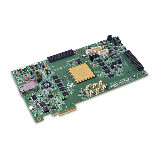
Introduction Introduction The Microsemi RTG4™ Field Programmable Gate Array (FPGA) Development Kit provides designers with an evaluation and development platform for applications such as data transmission, serial connectivity, bus interface, and high-speed designs using the RTG4 devices. The development board features an RT4G150 device offering 151,824 logic elements in a ceramic package with 1,657 pins. -
Page 9: Block Diagram
• Two FMC connectors with HPC pin-out for expansion. • RJ45 interface for 10/100/1000 Ethernet. • USB micro-AB connector. • Headers for SPI and GPIOs. • FTDI programmer interface to program the external SPI flash. UG0617 User Guide Revision 5.0... -
Page 10: Board Key Components
RTG4 Development Board Components Name Description RTG4 FPGA Microsemi RT4G150 device in a ceramic package with 1,657 pins. DDR3 synchronous 8 × 256 MB (256 MB Micron DDR3 memories MT41K256M8DA-125 IT:K) for storing data. dynamic random 2 × 256 MB (512 MB Micron DDR3 memory MT41K256M8DA-125 IT:K) for storing the ECC access memory bits. - Page 11 RVI Header RVI header for application programming and debug from Keil ULINK or IAR J-Link. Embedded FlashPro5 Embedded FlashPro5 for RTG4 programming and debugging with Microsemi tools. Future Technology FTDI programmer interface (J47) to program the external SPI flash. An FTDI chip is also used...
-
Page 12: Installation And Settings
FlashPro5 drivers. For instructions on how to install the Libero software and SoftConsole, see Libero Software Installation and Licensing Guide. For instructions on how to download and install Microsemi DirectCores, SGCores, and driver firmware cores, see Installing IP Cores and Drivers User Guide. In order to design with Microsemi FPGAs and SoC, these IP cores must be installed on the PC where Libero SoC is installed while designing with Microsemi FPGAs and SoCs. -
Page 13: Leds
For locations of various jumpers and test points on the RTG4 Development Board, see Figure 19, page 39. 3.2.2 LEDs The following table lists the power supply and Ethernet LEDs. Table 4 • LEDs Description DS12 VDD_REG supply DS13 1P5V_REG supply DS14 0P75V_REG_FDDR0 supply DS15 0P75V_REG_FDDR1 supply UG0617 User Guide Revision 5.0... -
Page 14: Test Points
TP1, TP2, TP76 TP14 VDD_REG TP12 3.3 V TP19 3P3V_LDO TP30 2P5V TP59 1.5 V TP57 0.75 V (FDDR0) TP69 0.75 V (FDDR1) TP18 VCCIO_HPC1_VAD VCCIO_HPC2_VAD TP43 1.8 V TP37 PHY 1.0 V TP48 1P2V_SERDES_IO UG0617 User Guide Revision 5.0... -
Page 15: Power Sources
2.5 V, 1.8 V, 1.5 V, or 1.2 V Bank9 1P5V_REG 2.5 V VDD_REG 1.2 V or 1.0 V 3.3 V VREF0 0P75V_VTT_REF_FDDR0 0.75 V VREF9 0P75V_VTT_REF_FDDR1 0.75 V SERDES_VDDI 2P5V 2.5 V VDDPLL 3P3V_LDO 3.3 V UG0617 User Guide Revision 5.0... -
Page 16: Figure 3 Voltage Rails In The Rtg4 Development Kit
2.5 V LDO – 5 A 2.5 V LDO for SERDES PLLs and FPGA Bank voltages MIC69502 WR – 5 A 1.2 V LDO – 1.5 A 1.2 V LDO for SERDES IOs MIC69153 YME – 1.5 A UG0617 User Guide Revision 5.0... -
Page 17: Key Components Description And Operation
For example, when the voltage measured across TP16 is 0.5 V, the core power consumed is 2.4 W. The following figure shows the on-board core power measurement circuity. Figure 5 • Core Power Measurement 12 V TP16 5.0 V Gain 1.2 V 1.2 V Regulator PTH08T230WAZ 0.05? _1% TP14 UG0617 User Guide Revision 5.0... -
Page 18: Memory Interface
CK, CK# Data DQ[31:0] DDR3 SDRAM 256 MB FDDR_W – Bank9 256MX8 DQS/DQS[3:0]# 4 memory chips 1 SECDED chip Address A[15:0] Control lines Note: DDR3 chip supports single bit error correction and dual bit error detection. UG0617 User Guide Revision 5.0... -
Page 19: Serdes Interface
The following figure shows the SERDES PCIe0 interface of the RTG4 Development Board. Figure 7 • SERDES_PCIe0 Interface Lane0/ RXD Lane1/ RXD Lane2/ RXD Lane3/ RXD RTG4 PCIe Edge SERDES_PCIe0 Connector Lane0/ TXD Lane1/ TXD Lane2/ TXD Lane3/ TXD REFCLK0 100 MHz Diff clock source UG0617 User Guide Revision 5.0... -
Page 20: Serdes1 And Serdes2 Interfaces
SERDES1 REFCLK0 SERDES2 REFCLK0 SERDES2 REFCLK0 According to the VITA-57 standard, series capacitors should be placed on the daughter board for TXD and RXD pins. For more information, see the Board Level Schematics document (provided separately). UG0617 User Guide Revision 5.0... -
Page 21: Table 7 Serdes1 And Serdes2 Interfaces-J12 Pinout
SERDES_2_RXD2_N HPC2_SERDES2_REFCLK0_P AR16 SERDES_2_REFCLK_P HPC2_SERDES2_REFCLK0_N AP16 SERDES_2_REFCLK_N HPC2_SERDES2_TXD3_P AU19 SERDES_2_TXD3_P HPC2_SERDES2_TXD3_N AT19 SERDES_2_TXD3_N HPC2_SERDES2_TXD2_P AW18 SERDES_2_TXD2_P HPC2_SERDES2_TXD2_N AV18 SERDES_2_TXD2_N HPC2_SERDES1_TXD0_P SERDES_1_TXD0_P HPC2_SERDES1_TXD0_N SERDES_1_TXD0_N HPC2_SERDES1_RXD0_P AV10 SERDES_1_RXD0_P HPC2_SERDES1_RXD0_N AW10 SERDES_1_RXD0_N HPC2_SERDES1_REFCLK0_P AR12 SERDES_1_REFCLK_P HPC2_SERDES1_REFCLK0_N AP12 SERDES_1_REFCLK_N UG0617 User Guide Revision 5.0... -
Page 22: Serdes3 And Serdes4 Interfaces
SERDES3 REFCLK0 SERDES4 REFCLK0 SERDES2 REFCLK0 According to the VITA-57 standard, series capacitors should be placed on the daughter board for TXD and RXD pins. For more information, see the Board Level Schematics document (provided separately). UG0617 User Guide Revision 5.0... -
Page 23: Table 8 Serdes3 And Serdes4 Interfaces-J34 Pinout
AP30 SERDES_4_REFCLK_P HPC1_SERDES4_REFCLK0_N AR30 SERDES_4_REFCLK_N HPC1_SERDES4_TXD3_P AT33 SERDES_4_TXD3_P HPC1_SERDES4_TXD3_N AU33 SERDES_4_TXD3_N HPC1_SERDES4_TXD2_P AT31 SERDES_4_TXD2_P HPC1_SERDES4_TXD2_N AU31 SERDES_4_TXD2_N HPC1_SERDES3_TXD0_P AT23 SERDES_3_TXD0_P HPC1_SERDES3_TXD0_N AU23 SERDES_3_TXD0_N HPC1_SERDES3_RXD0_P BA23 SERDES_3_RXD0_P HPC1_SERDES3_RXD0_N AY23 SERDES_3_RXD0_N HPC1_SERDES3_REFCLK0_P AP26 SERDES_3_REFCLK_P HPC1_SERDES3_REFCLK0_N AR26 SERDES_3_REFCLK_N UG0617 User Guide Revision 5.0... -
Page 24: Serdes Pcie5 Interface
LVDS differential inputs with a 100 Ω differential internal termination resistor. • RCLK—Gigabit recovered clock • SCLK—25 MHz synchronous input reference clock Expected reference clock (REF_CLK) specifications: • Voltage level: 3.3 (± 0.3) V • Differential LVDS UG0617 User Guide Revision 5.0... -
Page 25: Programming
RTG4 Programming Guide. The following figure shows the programming interface of the RTG4 Development Board. Figure 12 • Programming Interface Header Connector USB Mini-B RTG4 SC_SPI FT4232 Connector (J47) JTAG JTAG JTAG_SEL (Bank3) FP4/FP5 Header (J22) UG0617 User Guide Revision 5.0... -
Page 26: Ftdi Interface
The following figure shows the FTDI interface of the RTG4 Development Board. Figure 13 • FTDI Interface TXD—E28 MSIO RXD—E27 UART SCL—G30 MSIO SDA—G31 USB Mini-B RTG4 FT4232 Connector (J47) SC_SPI JTAG JTAG JTAG_SEL (Bank3) FP4/FP5 Header (J22) UG0617 User Guide Revision 5.0... -
Page 27: System Reset
An on-chip RTG4 PLL can be configured to generate a wide range of high-precision clock frequencies. Table 10 • 50 MHz Clock RTG4 Development Kit Pin RTG4 Package Pin Number RTG4 Device Pin Name 50MHZ_B1 AA39 MSIOD73PB1/GB12_23/CCC_NE0_CLKI2 UG0617 User Guide Revision 5.0... -
Page 28: User Interface
The board has eight-active high LEDs connected to the RTG4 device that can be used to debug applications. The following table lists the on-board user LEDs. Table 12 • LEDs RTG4 Development Kit Pin RTG4 Package Pin Number RTG4 Device Pin Name LED1 MSIOD62PB1 LED2 MSIOD46PB1 LED3 MSIOD47PB1 LED4 MSIOD46NB1 UG0617 User Guide Revision 5.0... -
Page 29: Push-Button Switches
The following figure shows the switches interface of the RTG4 Development Board. Figure 17 • Switches Interface 2.5 V SWITCH1 SWITCH2 RTG4 SWITCH3 SWITCH4 For more information, see the Board Level Schematics document (provided separately). UG0617 User Guide Revision 5.0... -
Page 30: Slide Switches - Dpdt
The following figure shows the SPST interface of the RTG4 Development Board. Figure 18 • SPST Interface 2.5 V DIP1 DIP2 DIP3 DIP4 RTG4 DIP5 DIP6 DIP7 DIP8 For more information, see the Board Level Schematics document (provided separately). UG0617 User Guide Revision 5.0... -
Page 31: Fmc Connectors
HPC1_SERDES4_TXD0_N AW28 SERDES_4_TXD0_N HPC1_SERDES4_TXD1_P AT29 SERDES_4_TXD1_P HPC1_SERDES4_TXD1_N AU29 SERDES_4_TXD1_N HPC1_CLK_DIR_B4 MSIO349PB4 HPC1_SERDES4_RXD3_P AW32 SERDES_4_RXD3_P HPC1_SERDES4_RXD3_N AV32 SERDES_4_RXD3_N HPC1_SERDES4_RXD2_P BA31 SERDES_4_RXD2_P HPC1_SERDES4_RXD2_N AY31 SERDES_4_RXD2_N HPC1_SERDES4_REFCLK0_P AP30 SERDES_4_REFCLK_P HPC1_SERDES4_REFCLK0_N AR30 SERDES_4_REFCLK_N HPC1_SERDES4_TXD3_P AT33 SERDES_4_TXD3_P HPC1_SERDES4_TXD3_N AU33 SERDES_4_TXD3_N UG0617 User Guide Revision 5.0... - Page 32 MSIO344PB4 HPC1_SDA MSIO344NB4 HPC1_GA0 MSIO319PB5 HPC1_PG_C2M HPC1_SERDES3_REFCLK0_P AP26 SERDES_3_REFCLK_P HPC1_SERDES3_REFCLK0_N AR26 SERDES_3_REFCLK_N HPC1_LA01_CC_P_B6 MSIO266PB6/GB7/CCC_SW1_ CLKI3/SPWR_SW1_1_RX_ DATA_P HPC1_LA01_CC_N_B6 MSIO266NB6/SPWR_SW1_1_ RX_DATA_N HPC1_LA05_P_B6 MSIO251PB6 HPC1_LA05_N_B6 MSIO251NB6 HPC1_LA09_P_B6 MSIO272PB6 HPC1_LA09_N_B6 MSIO272NB6 HPC1_LA13_P_B6 MSIO267PB6 HPC1_LA13_N_B6 MSIO267NB6 HPC1_LA17_CC_P_B6 MSIO253PB6/GB1/CCC_SW0_ CLKI2/SPWR_SW0_1_RX_ STROBE_P UG0617 User Guide Revision 5.0...
- Page 33 HPC1_HB03_N_B2 MSIOD9NB2 HPC1_HB05_P_B2 MSIOD19PB2 HPC1_HB05_N_B2 MSIOD19NB2 HPC1_HB09_P_B2 MSIOD7PB2 HPC1_HB09_N_B2 MSIOD7NB2 HPC1_HB13_P_B2 MSIOD10PB2 HPC1_HB13_N_B2 MSIOD10NB2 HPC1_HB19_P_B2 MSIOD8PB2 HPC1_HB19_N_B2 MSIOD8NB2 HPC1_HB21_P_B2 MSIOD17PB2 HPC1_HB21_N_B2 MSIOD17NB2 VCCIO_HPC1_VADJ HPC1_PG_M2C MSIO356PB4 HPC1_HA00_CC_P_B5 MSIO292PB5/GB9/GRESET HPC1_HA00_CC_N_B5 MSIO292NB5 HPC1_HA04_P_B5 MSIO296PB5 HPC1_HA04_N_B5 MSIO296NB5 HPC1_HA08_P_B5 MSIO299PB5 UG0617 User Guide Revision 5.0...
- Page 34 HPC1_HB16_N_B2 MSIOD16NB2 HPC1_HB20_P_B2 MSIOD2PB2 HPC1_HB20_N_B2 MSIOD2NB2 VCCIO_HPC1_VADJ HPC1_CLK1_M2C_P_B4 MSIO334PB4/GB17/CCC_SE0_ CLKI2/SPWR_SE0_1_RX_ STROBE_P HPC1_CLK1_M2C_N_B4 MSIO334NB4/SPWR_SE0_1_ RX_STROBE_N HPC1_LA00_CC_P_B6 MSIO254PB6/GB3/CCC_SW0_ CLKI3/SPWR_SW0_1_RX_ DATA_P HPC1_LA00_CC_N_B6 MSIO254NB6/SPWR_SW0_1_ RX_DATA_N HPC1_LA03_P_B6 MSIO242PB6 HPC1_LA03_N_B6 MSIO242NB6 HPC1_LA08_P_B6 MSIO260PB6 HPC1_LA08_N_B6 MSIO260NB6 HPC1_LA12_P_B6 MSIO269PB6 HPC1_LA12_N_B6 MSIO269NB6 HPC1_LA16_P_B6 MSIO268PB6 UG0617 User Guide Revision 5.0...
- Page 35 MSIO245NB6 HPC1_LA04_P_B6 MSIO258PB6 HPC1_LA04_N_B6 MSIO258NB6 HPC1_LA07_P_B6 MSIO257PB6 HPC1_LA07_N_B6 MSIO257NB6 HPC1_LA11_P_B6 MSIO273PB6 HPC1_LA11_N_B6 MSIO273NB6 HPC1_LA15_P_B6 MSIO259PB6 HPC1_LA15_N_B6 MSIO259NB6 HPC1_LA19_P_B6 MSIO256PB6 HPC1_LA19_N_B6 MSIO256NB6 HPC1_LA21_P_B6 MSIO247PB6 HPC1_LA21_N_B6 MSIO247NB6 HPC1_LA24_P_B6 MSIO250PB6 HPC1_LA24_N_B6 MSIO250NB6 HPC1_LA28_P_B6 MSIO241PB6 HPC1_LA28_N_B6 MSIO241NB6 HPC1_LA30_P_B6 MSIO249PB6 UG0617 User Guide Revision 5.0...
- Page 36 HPC1_HA22_N_B5 MSIO279NB5 HPC1_HB01_P_B2 MSIOD20PB2 HPC1_HB01_N_B2 MSIOD20NB2 HPC1_HB07_P_B2 MSIOD21PB2 HPC1_HB07_N_B2 MSIOD21NB2 HPC1_HB11_P_B2 MSIOD18PB2 HPC1_HB11_N_B2 MSIOD18NB2 HPC1_HB15_P_B2 MSIOD6PB2 HPC1_HB15_N_B2 MSIOD6NB2 HPC1_HB18_P_B2 MSIOD5PB2 HPC1_HB18_N_B2 MSIOD5NB2 VCCIO_HPC1_VIO_B_M2C_FMC VDDI2_1 VCCIO_HPC1_VIO_B_M2C_FMC VDDI2_1 HPC1_CLK2_BIDIR_P_B4 MSIO346PB4/GB21/CCC_SE1_ CLKI2/SPWR_SE1_1_RX_ STROBE_P HPC1_CLK2_BIDIR_N_B4 MSIO346NB4/SPWR_SE1_1_ RX_STROBE_N HPC1_HA02_P_B5 MSIO280PB5 UG0617 User Guide Revision 5.0...
-
Page 37: Table 16 J12 Fmc Connector Pinout
FMC connector for application development. The following table provides the J12 FMC pinout details. Table 16 • J12 FMC Connector Pinout FMC Pin Number—J12 FMC Net Name RTG4 Pin Number RTG4 Pin Name HPC2_SERDES1_RXD1_P AY11 SERDES_1_RXD1_P HPC2_SERDES1_RXD1_N BA11 SERDES_1_RXD1_N UG0617 User Guide Revision 5.0... - Page 38 HPC2_SERDES2_REFCLK0_N AP16 SERDES_2_REFCLK_N HPC2_SERDES2_TXD3_P AU19 SERDES_2_TXD3_P HPC2_SERDES2_TXD3_N AT19 SERDES_2_TXD3_N HPC2_SERDES2_TXD2_P AW18 SERDES_2_TXD2_P HPC2_SERDES2_TXD2_N AV18 SERDES_2_TXD2_N HPC2_SERDES1_TXD0_P SERDES_1_TXD0_P HPC2_SERDES1_TXD0_N SERDES_1_TXD0_N HPC2_SERDES1_RXD0_P AV10 SERDES_1_RXD0_P HPC2_SERDES1_RXD0_N AW10 SERDES_1_RXD0_N HPC2_LA06_P_B8 AB11 MSIOD176PB8 HPC2_LA06_N_B8 AB10 MSIOD176NB8 HPC2_LA10_P_B8 MSIOD179PB8 HPC2_LA10_N_B8 MSIOD179NB8 UG0617 User Guide Revision 5.0...
- Page 39 MSIOD189NB8 HPC2_LA09_P_B8 MSIOD172PB8 HPC2_LA09_N_B8 MSIOD172NB8 HPC2_LA13_P_B8 MSIOD195PB8 HPC2_LA13_N_B8 MSIOD195NB8 HPC2_LA17_CC_P_B8 MSIOD183PB8/GB0_11/CCC_ NW0_CLKI0/SPWR_NW0_0_ RX_STROBE_P HPC2_LA17_CC_N_B8 MSIOD183NB8/SPWR_NW0_0_ RX_STROBE_N HPC2_LA23_P_B8 MSIOD187PB8 HPC2_LA23_N_B8 MSIOD187NB8 HPC2_LA26_P_B8 MSIOD168PB8/GB0_11/CCC_ NW1_CLKI2/SPWR_NW1_1_ RX_STROBE_P HPC2_LA26_N_B8 MSIOD168NB8/SPWR_NW1_1_ RX_STROBE_N HPC2_GA1 MSIOD229NB7 HPC2_HB03_P_B7 MSIOD220PB7 HPC2_HB03_N_B7 MSIOD220NB7 HPC2_HB05_P_B7 MSIOD208PB7 UG0617 User Guide Revision 5.0...
- Page 40 RX_STROBE_N HPC2_HB04_P_B7 MSIOD212PB7 HPC2_HB04_N_B7 MSIOD212NB7 HPC2_HB08_P_B7 MSIOD222PB7 HPC2_HB08_N_B7 MSIOD222NB7 HPC2_HB12_P_B7 MSIOD205PB7 HPC2_HB12_N_B7 MSIOD205NB7 HPC2_HB16_P_B7 MSIOD207PB7 HPC2_HB16_N_B7 MSIOD207NB7 HPC2_HB20_P_B7 MSIOD216PB7 HPC2_HB20_N_B7 MSIOD216NB7 VCCIO_HPC2_VADJ AA13 VDDI8_1 HPC2_CLK1_M2C_P_B1 MSIOD43PB1/GB12_23/CCC_ NE0_CLKI0/SPWR_NE0_0_RX_ STROBE_P HPC2_CLK1_M2C_N_B1 MSIOD43NB1/SPWR_NE0_0_ RX_STROBE_N HPC2_LA00_CC_P_B8 MSIOD197PB8/GB0_11/CCC_ NW1_CLKI1/SPWR_NW1_0_ RX_DATA_P UG0617 User Guide Revision 5.0...
- Page 41 HPC2_LA33_N_B8 MSIOD180NB8 VCCIO_HPC2_VADJ AA13 VDDI8_1 HPC2_PRSNT_M2CL MSIO357NB4 HPC2_CLK0_M2C_P_B1 AA34 MSIOD59PB1/GB12_23/CCC_ NE1_CLKI1/SPWR_NE1_0_RX_ DATA_P HPC2_CLK0_M2C_N_B1 AB34 MSIOD59NB1/SPWR_NE1_0_ RX_DATA_N HPC2_LA02_P_B8 MSIOD178PB8 HPC2_LA02_N_B8 MSIOD178NB8 HPC2_LA04_P_B8 AA10 MSIOD184PB8 HPC2_LA04_N_B8 MSIOD184NB8 HPC2_LA07_P_B8 MSIOD194PB8 HPC2_LA07_N_B8 MSIOD194NB8 HPC2_LA11_P_B8 MSIOD170PB8 HPC2_LA11_N_B8 MSIOD170NB8 HPC2_LA15_P_B8 MSIOD169PB8 UG0617 User Guide Revision 5.0...
- Page 42 HPC2_HB01_P_B7 MSIOD215PB7 HPC2_HB01_N_B7 MSIOD215NB7 HPC2_HB07_P_B7 MSIOD224PB7 HPC2_HB07_N_B7 MSIOD224NB7 HPC2_HB11_P_B7 MSIOD217PB7 HPC2_HB11_N_B7 MSIOD217NB7 HPC2_HB15_P_B7 MSIOD206PB7 HPC2_HB15_N_B7 MSIOD206NB7 HPC2_HB18_P_B7 MSIOD209PB7 HPC2_HB18_N_B7 MSIOD209NB7 VCCIO_HPC2_VIO_B_M2C_FMC VDDI7_1 VCCIO_HPC2_VIO_B_M2C_FMC VDDI7_1 HPC2_CLK2_BIDIR_P_B1 MSIOD58PB1/GB12_23/CCC_ NE1_CLKI0/SPWR_NE1_0_RX_ STROBE_P HPC2_CLK2_BIDIR_N_B1 MSIOD58NB1/SPWR_NE1_0_ RX_STROBE_N HPC2_HB00_CC_P_B7 MSIOD218PB7/GB0_11/CCC_ SW1_CLKI1/SPWR_SW1_0_ RX_DATA_P UG0617 User Guide Revision 5.0...
- Page 43 Number—J12 FMC Net Name RTG4 Pin Number RTG4 Pin Name HPC2_HB00_CC_N_B7 MSIOD218NB7/SPWR_SW1_0_ RX_DATA_N HPC2_HB06_CC_P_B7 MSIOD228PB7/GB0_11/CCC_ SW0_CLKI0/SPWR_SW0_0_ RX_STROBE_P HPC2_HB06_CC_N_B7 MSIOD228NB7/SPWR_SW0_0_ RX_STROBE_N HPC2_HB10_P_B7 MSIOD210PB7 HPC2_HB10_N_B7 MSIOD210NB7 HPC2_HB14_P_B7 MSIOD211PB7 HPC2_HB14_N_B7 MSIOD211NB7 HPC2_HB17_CC_P_B7 MSIOD227PB7/GB0_11/CCC_ SW0_CLKI1/SPWR_SW0_0_ RX_DATA_P HPC2_HB17_CC_N_B7 MSIOD227NB7/SPWR_SW0_0_ RX_DATA_N VCCIO_HPC2_VIO_B_M2C_FMC VDDI7_1 UG0617 User Guide Revision 5.0...
-
Page 44: Pin List
Pin List Pin List For the RTG4 Development Board pin list, see the CG1657 Package Pin Assignment Table at http://www.microsemi.com/document-portal/doc_download/134616-cg1657-package-pin-assignment- table. UG0617 User Guide Revision 5.0... -
Page 45: Board Components Placement
0P75V_REG_FDDR1 C103 TP68 TP67 3P3V R101 5V0_FT R102 C101 SERDES5_RX0_P SERDES5_TX0_P R104 C110 C104 TP72 C105 TP76 C107 C106 TP77 TP78 C108 C109 R110 C111 TP79 R122 TP82 TP81 3P3V S0_PRSNT R123 REFCLK_N TP80 CON1 UG0617 User Guide Revision 5.0... -
Page 46: Figure 20 Rtg4 Development Kit Silkscreen Bottom View
C803 C779 C800 R348 C777 C809 C810 R331 C811 R351 C793 C794 C581 C582 R260 R357 Y5 R270 R268 100MHz C615 C616 C815 C641 R363 C653 R371 C668 C817 C818 R366 C816 R365 R369 R373 UG0617 User Guide Revision 5.0... - Page 47 DG0622: RTG4 FPGA PCIe Data Plane Demo using Two Channel Fabric DMA Demo Guide • LG0623: RTG4 FPGA Fabric Lab Guide • DG0630: RTG4 FPGA DSP FIR Filter Demo Guide • DG0625: Interfacing RTG4 FPGA with the External DDR3 Memory Through FDDR Demo Guide UG0617 User Guide Revision 5.0...
- Page 48 Once the USB cable is connected, the PC will detect the on-board embedded FP5 and install the drivers. Note: Installing drivers is a one-time process. UG0617 User Guide Revision 5.0...
-
Page 49: Figure 21 Flashpro Window
Figure 21 • FlashPro Window Click New Project to create a new project, as shown in Figure 22, page 44. • Enter the Project Name. • Select Single device as the Programming mode, then click OK. UG0617 User Guide Revision 5.0... -
Page 50: Figure 22 Creating A New Project
Click Browse, then select the uprom Boot mtd 40KB uPROM Final.stp file from the Load Programming File window. Figure 23 • Configuring the Device Click Program to program the device. When the device is programmed successfully, the status Run Program PASSED is displayed. UG0617 User Guide Revision 5.0...
Need help?
Do you have a question about the UG0617 and is the answer not in the manual?
Questions and answers