Table of Contents
Advertisement
Quick Links
Advertisement
Table of Contents

Subscribe to Our Youtube Channel
Related Manuals for Microsemi UG0557


Summary of Contents for Microsemi UG0557
- Page 1 UG0557 User Guide SmartFusion2 SoC FPGA Advanced Development Kit...
- Page 2 Within the USA: +1 (800) 713-4113 with the Buyer. Microsemi does not grant, explicitly or implicitly, to any party any patent rights, licenses, or any other IP rights, whether with regard to such information itself or anything described by such information. Information provided in this...
-
Page 3: Table Of Contents
5 Pin List ............41 UG0557 User Guide Revision 4.0... - Page 4 Running the Test ............51 UG0557 User Guide Revision 4.0...
- Page 5 SerDes Loopback Passed ............57 UG0557 User Guide Revision 4.0...
- Page 6 Jumper Settings for Manufacturing Test ..........50 UG0557 User Guide Revision 4.0...
-
Page 7: Revision History
Validating Power Supply, page 46 (SAR 61171). • Information about FMC connectors was updated. For more information, see FMC Connectors, page 25 (SAR 67950). Revision 1.0 Revision 1.0 was the first publication of this document. UG0557 User Guide Revision 4.0... -
Page 8: Introduction
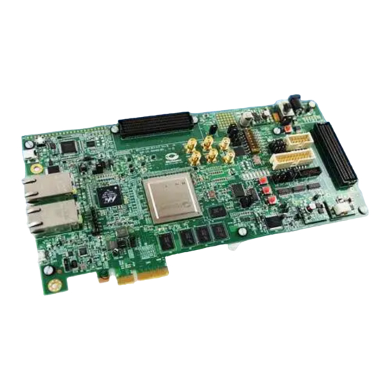
USB A to Mini B cable 12 V/5 A power adapter Block Diagram The following figure is the block diagram of the SmartFusion2 Advanced Development Kit. Figure 1 • SmartFusion2 Advanced Development Kit Block Diagram UG0557 User Guide Revision 4.0... -
Page 9: Web Resources
HPC (J30), and although the bread board connector (J350) space available for Bank 4 (MSIO) pins. The SmartFusion2 device can be programmed through embedded FlashPro5. The Advanced Development Kit has the current measurement feature (see Current Measurement, page 11). UG0557 User Guide Revision 4.0... -
Page 10: Board Key Components
FTDI programmer interface (J33) to program the external SPI flash. An FTDI International (FTDI) programmer chip is also used to change the JTAG_SEL signal (high or low) remotely for switching between the RVI header and JTAG mode. UG0557 User Guide Revision 4.0... - Page 11 (MR) pin drops to a logical low. I2C port header 16-pin header available for I2C0 and I2C1 interfaces of the SmartFusion2 device. UG0557 User Guide Revision 4.0...
-
Page 12: Installation And Settings
Libero Software Installation and Licensing Guide. For instructions on how to download and install Microsemi DirectCores, SGCores, and driver firmware cores, which must be installed on the PC where Libero SoC is installed, see Installing IP Cores and Drivers User Guide. - Page 13 Pin 2-3 for JTAG programming via FP4. Closed J125 Jumper to select FTDI SPI-0 or FTDI SPI-1 Pin 1-2 for FTDI SPI-1 slave Open slave programming programming. Pin 2-3 for FTDI SPI-0 slave Open programming. UG0557 User Guide Revision 4.0...
-
Page 14: Leds
Indicates that DS13 is connected to parallel LED output port 1 (P1_LED[1]) of Marvell PHY DS12 Indicates that DS12 is connected to parallel LED output port 1 (P1_LED[2]) of Marvell PHY DS11 Indicates that DS11 is connected to parallel LED output port 1 (P1_LED[3]) of Marvell PHY UG0557 User Guide Revision 4.0... -
Page 15: Test Points
2.5 V Bank11 VCCIO_HPC_VADJ 3.3 V, 2.5 V, 1.8 V, 1.5 V, or 1.2 V Bank12 2P5V_LDO 2.5 V Bank13 2P5V_LDO 2.5 V Bank14 VCCIO_HPC_VADJ 3.3 V, 2.5 V, 1.8 V, 1.5 V, or 1.2 V UG0557 User Guide Revision 4.0... -
Page 16: Figure 3 Voltage Rails In Smartfusion2 Advanced Development Kit
The following figure shows the voltage rails (12 V, 5 V, 3.3 V, 2.5 V, 1.8 V, 1.5 V, 1.2 V, 1.0 V, and 0.75 V) available in the SmartFusion2 Advanced Development Kit. Figure 3 • Voltage Rails in SmartFusion2 Advanced Development Kit UG0557 User Guide Revision 4.0... -
Page 17: Key Components Description And Operation
Measure the output voltage (V ) at TP17. I = (V /5). Core power consumed (P) = (1.2 V) × I. For example, when the voltage measured across TP17 is 0.5 V, the core power consumed is 0.12 W. UG0557 User Guide Revision 4.0... -
Page 18: Current Sensing For Flash*Freeze Mode
DDR3 SDRAM specifications for the SmartFusion2 device are as follows. • MT46H32M16LF: 32 Meg × 8 × 8 banks • Density: 256 MB • Clock rate: 800 MHz • Data rate: DDR3 - 1600 • Total capacity: 1 GB across four chips UG0557 User Guide Revision 4.0... -
Page 19: Figure 6 Smartfusion2 Memory Interface
Key Components Description and Operation The following figure shows the SmartFusion2 memory interface. Figure 6 • SmartFusion2 Memory Interface For more information, see the Board Level Schematics document (provided separately). UG0557 User Guide Revision 4.0... -
Page 20: Serdes Interface
The following figure shows the SERDES0 interface of the SmartFusion2 Advanced Development Board. Figure 7 • SERDES0 Interface Note: Mount R977 and R978 to source the clock from 100 MHz differential oscillator to the SERDES0 REFCLK1. UG0557 User Guide Revision 4.0... -
Page 21: Serdes1 Interface
SmartFusion2 Advanced Development Kit board pins AF18 and AG18. The following figure shows the SERDES1 interface of the SmartFusion2 Advanced Development Board. Figure 8 • SERDES1 Interface UG0557 User Guide Revision 4.0... -
Page 22: Serdes2 Interface
SmartFusion2 Advanced Development Kit board pins AE17 and AF17. The following figure shows the SERDES2 interface of the SmartFusion2 Advanced Development Board. Figure 9 • SERDES2 Interface UG0557 User Guide Revision 4.0... -
Page 23: Serdes3 Interface
SERDES3 reference clock 0 is connected from FMC connector or SMA connector through MUX. • SERDES3 reference clock 1 is connected from 125 MHz or 100 MHz through MUX. The following figure shows the SERDES3 interface of the SmartFusion2 Advanced Development Board. Figure 10 • SERDES3 Interface UG0557 User Guide Revision 4.0... -
Page 24: Usb Interface
•Rise/fall time: Maximum 1 ns @ 20% to 80% of supply (3.3 V) •Output voltage levels: 0 = 0.90 minimum, 1.10 typical; 1 = 1.43 typical, 1.60 maximum •Differential output voltage: 247 mV minimum, 454 mV maximum UG0557 User Guide Revision 4.0... -
Page 25: Programming
The dedicated programming SPI port can operate in SPI slave or SPI master modes. For more information, see SmartFusion2 and IGLOO2 Programming User Guide. The following figure shows the programming interface of the SmartFusion2 Advanced Development Board. Figure 13 • Programming Interface UG0557 User Guide Revision 4.0... -
Page 26: Ftdi Interface
DS1818 maintains reset till 150 milliseconds after the 3.3 V supply returns to intolerance. The TPS3808G09DBVR device monitors the voltage at the VDD_REG terminal. If the voltage at this terminal sense-drops below the threshold voltage of 0.9 V, the M2S_RSTB signal is asserted. UG0557 User Guide Revision 4.0... -
Page 27: Clock Sources
SmartFusion2 Device Pin Name 50MHZ_SECLK_B4_P1 MSIO39PB4/CCC_NE0_CLKI1 The following figure shows the 50 MHz clock oscillator interface. Figure 15 • 50 MHz Clock Oscillator Interface For more information, see the Board Level Schematics document (provided separately). UG0557 User Guide Revision 4.0... -
Page 28: 100 Mhz Clock Oscillator
The board has eight active-high LEDs connected to the SmartFusion2 device that can be used to debug applications. The following table lists the on-board user LEDs. Table 10 • LEDs SmartFusion2 Advanced SmartFusion2 SmartFusion2 Device Development Board Pin Package Pin Number Pin Name DDRIO149PB1/FDDR_DQS2 DDRIO150PB1/FDDR_DQ18 DDRIO148PB1/FDDR_DM_RD DDRIO149NB1/FDDR_DQS2_N DDRIO151PB1/FDDR_DQ16 DDRIO148NB1/FDDR_DQ20 DDRIO151NB1/FDDR_DQ17 DDRIO150NB1/FDDR_DQ19 UG0557 User Guide Revision 4.0... -
Page 29: Push-Button Switches
SWITCH3 DDRIO157PB1/FDDR_DQ8 SWITCH4 DDRIO157NB1/FDDR_DQ9 System Reset The following figure shows the switches interface of the SmartFusion2 Advanced Development Board. Figure 18 • Switches Interface For more information, see the Board Level Schematics document (provided separately). UG0557 User Guide Revision 4.0... -
Page 30: Slide Switches - Dpdt
DIP5 DDRIO154NB1/FDDR_DM_RDQS1 DIP6 DDRIO155PB1/FDDR_DQS1 DIP7 DDRIO155NB1/FDDR_DQS1_N The following figure shows the SPST interface of the SmartFusion2 Advanced Development Board. Figure 19 • SPST Interface For more information, see the Board Level Schematics document (provided separately). UG0557 User Guide Revision 4.0... -
Page 31: Fmc Connectors
AM15 SERDES_2_RXD1_P FMC_HPC_SERDES2_RXD1_N AL15 SERDES_2_RXD1_N FMC_HPC_SERDES2_RXD0_P AM17 SERDES_2_RXD0_P FMC_HPC_SERDES2_RXD0_N AL17 SERDES_2_RXD0_N FMC_HPC_SERDES1_RXD3_P AL19 SERDES_1_RXD3_P FMC_HPC_SERDES1_RXD3_N AM19 SERDES_1_RXD3_N FMC_HPC_SERDES1_RXD2_P AL21 SERDES_1_RXD2_P FMC_HPC_SERDES1_RXD2_N AM21 SERDES_1_RXD2_N FMC_HPC_SERDES2_TXD2_P AN12 SERDES_2_TXD2_P FMC_HPC_SERDES2_TXD2_N AP12 SERDES_2_TXD2_N FMC_HPC_SERDES2_TXD1_P AN14 SERDES_2_TXD1_P FMC_HPC_SERDES2_TXD1_N AP14 SERDES_2_TXD1_N UG0557 User Guide Revision 4.0... - Page 32 AN16 SERDES_2_TXD0_P FMC_HPC_SERDES2_TXD0_N AP16 SERDES_2_TXD0_N FMC_HPC_SERDES1_TXD3_P AP18 SERDES_1_TXD3_P FMC_HPC_SERDES1_TXD3_N AN18 SERDES_1_TXD3_N FMC_HPC_SERDES1_TXD2_P AP20 SERDES_1_TXD2_P FMC_HPC_SERDES1_TXD2_N AN20 SERDES_1_TXD2_N FMC_HPC_SERDES1_RXD0_P AL25 SERDES_1_RXD0_P FMC_HPC_SERDES1_RXD0_N AM25 SERDES_1_RXD0_N FMC_HPC_SERDES1_RXD1_P AL23 SERDES_1_RXD1_P FMC_HPC_SERDES1_RXD1_N AM23 SERDES_1_RXD1_N FMC_HPC_SERDES1_REFCLK0_P AJ22 MSIOD271PB12/SERDES_1_REFCLK0_P FMC_HPC_SERDES1_REFCLK0_N AK22 MSIOD271NB12/SERDES_1_REFCLK0_N UG0557 User Guide Revision 4.0...
- Page 33 SERDES_1_TXD0_N FMC_HPC_SERDES1_TXD1_P AP22 SERDES_1_TXD1_P FMC_HPC_SERDES1_TXD1_N AN22 SERDES_1_TXD1_N FMC_HPC_SERDES2_TXD3_P AN10 SERDES_2_TXD3_P FMC_HPC_SERDES2_TXD3_N AP10 SERDES_2_TXD3_N FMC_HPC_SERDES2_RXD3_P AM11 SERDES_2_RXD3_P FMC_HPC_SERDES2_RXD3_N AL11 SERDES_2_RXD3_N HPC_LA06_M32_191P_B18 MSIO191PB18 HPC_LA06_M31_191N_B18 MSIO191NB18 HPC_LA10_T23_206P_B17 MSIO206PB17 HPC_LA10_T24_206N_B17 MSIO206NB17 HPC_LA14_P29_198P_B17 MSIO198PB17 HPC_LA14_P28_198N_B17 MSIO198NB17 HPC_LA18_CC_U29_215P_B17 MSIO215PB17/CCC_NW1_CLKI0 HPC_LA18_CC_U30_215N_B17 MSIO215NB17 UG0557 User Guide Revision 4.0...
- Page 34 MSIO81PB3/I2C_0_SDA/GPIO_30_B/USB_ DATA0_C 12P0V 12P0V 3P3V HPC_PG_C2M_H6_77N_B3 MSIO77NB3/MMUART_0_DSR/GPIO_20_B FMC_HPC_SERDES2_REFCLK0_P AK14 MSIOD277PB10/SERDES_2_REFCLK0_P FMC_HPC_SERDES2_REFCLK0_N AJ14 MSIOD277NB10/SERDES_2_REFCLK0_N HPC_LA01_CC_U27_216P_B17 MSIO216PB17/CCC_NW0_CLKI0 HPC_LA01_CC_U26_216N_B17 MSIO216NB17 HPC_LA05_N23_186P_B18 MSIO186PB18 HPC_LA05_N24_186N_B18 MSIO186NB18 HPC_LA09_R23_200P_B17 MSIO200PB17 HPC_LA09_R24_200N_B17 MSIO200NB17 HPC_LA13_R26_202P_B17 MSIO202PB17 HPC_LA13_R25_202N_B17 MSIO202NB17 HPC_LA17_CC_U31_213P_B17 MSIO213PB17/GB6/CCC_NW1_CLKI1 HPC_LA17_CC_U32_213N_B17 MSIO213NB17 HPC_LA23_T33_212P_B17 MSIO212PB17 UG0557 User Guide Revision 4.0...
- Page 35 HPC_TMS HPC_TRST_L 3P3V 3P3V 3P3V HPC_HA01_CC_AF16_276P_B11 AF16 MSIO276PB11/GB11/VCCC_SE0_CLKI HPC_HA01_CC_AG16_276N_B11 AG16 MSIO276NB11 HPC_HA05_AA3_17P_B6 MSIO17PB6 HPC_HA05_AA2_17N_B6 MSIO17NB6 HPC_HA09_AJ2_285P_B8 MSIO285PB8 HPC_HA09_AH3_285N_B8 MSIO285NB8 HPC_HA13_AH6_283P_B8 MSIO283PB8 HPC_HA13_AH5_283N_B8 MSIO283NB8 HPC_HA16_AG7_284P_B8 MSIO284PB8 HPC_HA16_AF7_284N_B8 MSIO284NB8 HPC_HA20_AB8_8P_B6 MSIO8PB6 HPC_HA20_AB7_8N_B6 MSIO8NB6 HPC_HB03_W1_20P_B5 MSIO20PB5 HPC_HB03_W2_20N_B5 MSIO20NB5 UG0557 User Guide Revision 4.0...
- Page 36 HPC_HB19_G31_175N_B0 MSIO175NB0 HPC_HB21_L25_174P_B0 MSIO174PB0 HPC_HB21_L26_174N_B0 MSIO174NB0 VCCIO_HPC_VADJ HPC_PG_M2C_J6_78P_B3 MSIO78PB3/MMUART_0_RI/GPIO_21_B HPC_HA00_CC_AJ4_282P_B8 MSIO282PB8/VCCC_SE1_CLKI HPC_HA00_CC_AJ3_282N_B8 MSIO282NB8 HPC_HA04_AG3_287P_B8 MSIO287PB8 HPC_HA04_AG4_287N_B8 MSIO287NB8 HPC_HA08_AD1_9P_B6 MSIO9PB6 HPC_HA08_AC1_9N_B6 MSIO9NB6 HPC_HA12_AE4_4P_B6 MSIO4PB6 HPC_HA12_AD4_4N_B6 MSIO4NB6 HPC_HA15_AA7_15P_B6 MSIO15PB6 HPC_HA15_Y7_15N_B6 MSIO15NB6 HPC_HA19_AB10_11P_B6 AB10 MSIO11PB6 HPC_HA19_AA10_11N_B6 AA10 MSIO11NB6 UG0557 User Guide Revision 4.0...
- Page 37 HPC_HB16_Y12_21P_B5 MSIO21PB5 HPC_HB16_Y11_21N_B5 MSIO21NB5 HPC_HB20_W12_28P_B5 MSIO28PB5/USB_XCLK_B HPC_HB20_W11_28N_B5 MSIO28NB5/USB_DIR_B VCCIO_HPC_VADJ HPC_CLK1_M2C_AH28_267P_B14 AH28 MSIO267PB14/CCC_SW0_CLKI2 HPC_CLK1_M2C_AG27_267N_B14 AG27 MSIO267NB14 HPC_LA00_CC_U23_214P_B17 MSIO214PB17/GB2/CCC_NW0_CLKI1 HPC_LA00_CC_U24_214N_B17 MSIO214NB17 HPC_LA03_N32_201P_B17 MSIO201PB17 HPC_LA03_N31_201N_B17 MSIO201NB17 HPC_LA08_M25_181P_B18 MSIO181PB18 HPC_LA08_M24_181N_B18 MSIO181NB18 HPC_LA12_M27_183P_B18 MSIO183PB18 HPC_LA12_M26_183N_B18 MSIO183NB18 HPC_LA16_T28_209P_B17 MSIO209PB17 HPC_LA16_T27_209N_B17 MSIO209NB17 UG0557 User Guide Revision 4.0...
- Page 38 MSIO194NB18 HPC_LA31_H34_196P_B18 MSIO196PB18 HPC_LA31_G34_196N_B18 MSIO196NB18 HPC_LA33_E33_176P_B18 MSIO176PB18 HPC_LA33_D33_176N_B18 MSIO176NB18 VCCIO_HPC_VADJ N36608719 HPC_PRSNT_M2CL_J7_78N_B3 MSIO78NB3/MMUART_0_DCD/GPIO_22_B HPC_CLK0_M2C_AJ6_281P_B8 MSIO281PB8/GB15/VCCC_SE1_CLKI HPC_CLK0_M2C_AJ5_281N_B8 MSIO281NB8 HPC_LA02_K31_179P_B18 MSIO179PB18 HPC_LA02_K30_179N_B18 MSIO179NB18 HPC_LA04_L30_182P_B18 MSIO182PB18 HPC_LA04_L29_182N_B18 MSIO182NB18 HPC_LA07_P23_192P_B18 MSIO192PB18 HPC_LA07_P24_192N_B18 MSIO192NB18 HPC_LA11_T30_210P_B17 MSIO210PB17 HPC_LA11_T29_210N_B17 MSIO210NB17 HPC_LA15_M30_188P_B18 MSIO188PB18 UG0557 User Guide Revision 4.0...
- Page 39 HPC_LA30_F33_185N_B18 MSIO185NB18 HPC_LA32_D34_180P_B18 MSIO180PB18 HPC_LA32_C34_180N_B18 MSIO180NB18 VCCIO_HPC_VADJ HPC_CLK3_M2C_P AK12 MSIOD278PB10/SERDES_2_REFCLK1_P HPC_CLK3_M2C_P AE17 MSIO275PB11/VCCC_SE0_CLKI HPC_CLK3_M2C_N AJ12 MSIOD278NB10/SERDES_2_REFCLK1_N HPC_CLK3_M2C_N AF17 MSIO275NB11 HPC_HA03_AA4_12P_B6 MSIO12PB6 HPC_HA03_AA5_12N_B6 MSIO12NB6 HPC_HA07_AC3_10P_B6 MSIO10PB6 HPC_HA07_AB3_10N_B6 MSIO10NB6 HPC_HA11_AD3_5P_B6 MSIO5PB6 HPC_HA11_AD2_5N_B6 MSIO5NB6 HPC_HA14_AG6_286P_B8 MSIO286PB8 HPC_HA14_AG5_286N_B8 MSIO286NB8 UG0557 User Guide Revision 4.0...
- Page 40 MSIO23PB5 HPC_HB11_W7_23N_B5 MSIO23NB5 HPC_HB15_V9_34P_B5 MSIO34PB5 HPC_HB15_V10_34N_B5 MSIO34NB5 HPC_HB18_T2_31P_B5 MSIO31PB5/USB_DATA2_B HPC_HB18_T3_31N_B5 MSIO31NB5/USB_DATA3_B VCCIO_HPC_VIO_B_M2C_FMC N36626276 HPC_CLK2_M2C_P AJ20 MSIOD272PB12/SERDES_1_REFCLK1_P HPC_CLK2_M2C_P AF18 MSIO274PB11/CCC_SW1_CLKI2 HPC_CLK2_M2C_N AK20 MSIOD272NB12/SERDES_1_REFCLK1_N HPC_CLK2_M2C_N AG18 MSIO274NB11/CCC_SW1_CLKI3 HPC_HA02_AB2_16P_B6 MSIO16PB6 HPC_HA02_AB1_16N_B6 MSIO16NB6 HPC_HA06_AC5_6P_B6 MSIO6PB6 HPC_HA06_AC4_6N_B6 MSIO6NB6 HPC_HA10_AE6_288P_B8 MSIO288PB8 UG0557 User Guide Revision 4.0...
- Page 41 MSIO268PB14/GB3/CCC_SW0_CLKI3 HPC_HA17_CC_AJ28_268N_B14 AJ28 MSIO268NB14 HPC_HA21_AA12_14P_B6 AA12 MSIO14PB6 HPC_HA21_AA11_14N_B6 AA11 MSIO14NB6 HPC_HA23_AB5_7P_B6 MSIO7PB6 HPC_HA23_AB6_7N_B6 MSIO7NB6 HPC_HB00_CC_F32_172P_B0 MSIO172PB0/GB0/CCC_NW0_CLKI3 HPC_HB00_CC_E32_172N_B0 MSIO172NB0 HPC_HB06_CC_J29_170P_B0 MSIO170PB0/CCC_NW1_CLKI3 HPC_HB06_CC_J28_170N_B0 MSIO170NB0 HPC_HB10_Y10_22P_B5 MSIO22PB5 HPC_HB10_Y9_22N_B5 MSIO22NB5 HPC_HB14_V6_33P_B5 MSIO33PB5/USB_DATA6_B HPC_HB14_U6_33N_B5 MSIO33NB5 HPC_HB17_CC_U5_37P_B5 MSIO37PB5/GB9/VCCC_SE0_CLKI HPC_HB17_CC_T5_37N_B5 MSIO37NB5 VCCIO_HPC_VIO_B_M2C_FMC UG0557 User Guide Revision 4.0...
-
Page 42: Table 14 Fmc Lpc Connector (J60) Pinout
SERDES_3_RXD0_P FMC_LPC_SERDES3_RXD0_P SERDES_3_RXD0_N FMC_LPC_SERDES3_RXD0_N AF33 MSIOD248PB15 LPC_LA06_AF33_248P_B15 AE33 MSIOD248NB15 LPC_LA06_AE33_248N_B15 AE30 MSIOD250PB15 LPC_LA10_AE30_250P_B15 AD30 MSIOD250NB15 LPC_LA10_AD30_250N_B15 MSIOD227PB16 LPC_LA14_W23_227P_B16 MSIOD227NB16 LPC_LA14_W24_227N_B16 AA32 MSIOD228PB16 LPC_LA18_CC_AA32_228P_B16 MSIOD228NB16 LPC_LA18_CC_Y32_228N_B16 MSIOD223PB16 LPC_LA27_V29_223P_B16 MSIOD223NB16 LPC_LA27_V28_223N_B16 MSIO45NB4/I2C_1_SCL/GPIO_1_A/U I2C1_SCL SB_DATA4_A MSIO45PB4/I2C_1_SDA/GPIO_0_A/U I2C1_SDA SB_DATA3_A UG0557 User Guide Revision 4.0... - Page 43 AK10 MSIOD279NB9/SERDES_3_REFCLK0 FMC_LPC_SERDES3_REFCLK0_N MSIOD219PB16/CCC_SW1_CLKI0 LPC_LA01_CC_W34_219P_B16 MSIOD219NB16 LPC_LA01_CC_V34_219N_B16 MSIOD226PB16 LPC_LA05_W29_226P_B16 MSIOD226NB16 LPC_LA05_W30_226N_B16 MSIOD231PB16 LPC_LA09_Y28_231P_B16 MSIOD231NB16 LPC_LA09_W28_231N_B16 AC24 MSIOD258PB15 LPC_LA13_AC24_258P_B15 AC23 MSIOD258NB15 LPC_LA13_AC23_258N_B15 MSIOD220PB16/CCC_SW0_CLKI0 LPC_LA17_CC_V23_220P_B16 MSIOD220NB16 LPC_LA17_CC_V24_220N_B16 AG32 MSIOD252PB15 LPC_LA23_AG32_252P_B15 AF32 MSIOD252NB15 LPC_LA23_AF32_252N_B15 MSIOD222PB16 LPC_LA26_V27_222P_B16 MSIOD222NB16 LPC_LA26_V26_222N_B16 UG0557 User Guide Revision 4.0...
- Page 44 LPC_LA00_CC_Y33_224P_B16 MSIOD224NB16 LPC_LA00_CC_W33_224N_B16 AC34 MSIOD232PB16 LPC_LA03_AC34_232P_B16 AB34 MSIOD232NB16 LPC_LA03_AB34_232N_B16 AC32 MSIOD233PB16 LPC_LA08_AC32_233P_B16 AC33 MSIOD233NB16 LPC_LA08_AC33_233N_B16 MSIOD229PB16 LPC_LA12_W26_229P_B16 MSIOD229NB16 LPC_LA12_W25_229N_B16 MSIOD234PB16 LPC_LA16_Y23_234P_B16 MSIOD234NB16 LPC_LA16_Y24_234N_B16 AF27 MSIOD257PB15 LPC_LA20_AF27_257P_B15 AE27 MSIOD257NB15 LPC_LA20_AE27_257N_B15 AG34 MSIOD244PB15 LPC_LA22_AG34_244P_B15 AF34 MSIOD244NB15 LPC_LA22_AF34_244N_B15 UG0557 User Guide Revision 4.0...
- Page 45 MSIOD225PB16 LPC_LA02_AA33_225P_B16 AA34 MSIOD225NB16 LPC_LA02_AA34_225N_B16 AD33 MSIOD239PB16 LPC_LA04_AD33_239P_B16 AD34 MSIOD239NB16 LPC_LA04_AD34_239N_B16 AE31 MSIOD247PB15 LPC_LA07_AE31_247P_B15 AE32 MSIOD247NB15 LPC_LA07_AE32_247N_B15 AF30 MSIOD254PB15 LPC_LA11_AF30_254P_B15 AG31 MSIOD254NB15 LPC_LA11_AG31_254N_B15 AF28 MSIOD256PB15 LPC_LA15_AF28_256P_B15 AE28 MSIOD256NB15 LPC_LA15_AE28_256N_B15 AG30 MSIOD260PB15 LPC_LA19_AG30_260P_B15 AF29 MSIOD260NB15 LPC_LA19_AF29_260N_B15 UG0557 User Guide Revision 4.0...
- Page 46 FMC LPC Connector (J60) Pinout (continued) MSIOD221PB16 LPC_LA21_W31_221P_B16 MSIOD221NB16 LPC_LA21_V31_221N_B16 AD28 MSIOD249PB15 LPC_LA24_AD28_249P_B15 AD29 MSIOD249NB15 LPC_LA24_AD29_249N_B15 AB25 MSIOD246PB15 LPC_LA28_AB25_246P_B15 AB26 MSIOD246NB15 LPC_LA28_AB26_246N_B15 AC25 MSIOD253PB15 LPC_LA30_AC25_253P_B15 AC26 MSIOD253NB15 LPC_LA30_AC26_253N_B15 AE26 MSIOD259PB15 LPC_LA32_AE26_259P_B15 AD26 MSIOD259NB15 LPC_LA32_AD26_259N_B15 VCCIO_LPC_VADJ UG0557 User Guide Revision 4.0...
-
Page 47: Pin List
Pin List Pin List The SmartFusion2 Advanced Development Kit uses an M2S150TS-1FCG1152 device. For a list of all package pins in this device, see SmartFusion2 FC1152 Pinouts. UG0557 User Guide Revision 4.0... -
Page 48: Board Components Placement
Board Components Placement Board Components Placement The following figure shows the placement of various components on the SmartFusion2 Advanced Development Kit silkscreen. UG0557 User Guide Revision 4.0... -
Page 49: Figure 20 Silkscreen Top View
Board Components Placement Figure 20 • Silkscreen Top View UG0557 User Guide Revision 4.0... -
Page 50: Figure 21 Silkscreen Bottom View
Board Components Placement The following figure shows the bottom view of the SmartFusion2 Advanced Development Kit silkscreen. Figure 21 • Silkscreen Bottom View UG0557 User Guide Revision 4.0... -
Page 51: Demo Design
PCIe interface of the SmartFusion2 device. The following figure shows the PCIe demo design window. Figure 22 • PCIe Demo Design Window For more information about running the demo design, see SmartFusion2 SoC FPGA PCIe Control Plane Demo Guide for Advanced Development Kit. UG0557 User Guide Revision 4.0... -
Page 52: Manufacturing Test
Short the J32 jumper to position 1-2. Connect one end of the mini USB to Type A USB cable to the J33 jumper, and other end to the USB port of the host PC. Launch the FlashPro v11.4 software. UG0557 User Guide Revision 4.0... -
Page 53: Figure 23 Flashpro Window
Click New Project to create a new project. In the New Project window, do the following, and click OK. • Enter a project name. • Select Single device as the programming mode. Figure 24 • New Project Window Click Configure Device. UG0557 User Guide Revision 4.0... -
Page 54: Running The Manufacturing Test
Connect one end of the mini USB to Type A USB cable to J33, and other end to the USB port of the host PC. Launch Tera Term from the Start menu. Figure 26 • Tera Term New Connection Window Select the Serial radio button. Select a port from the Port drop-down list, and click OK. UG0557 User Guide Revision 4.0... -
Page 55: Figure 27 Tera Term New Connection Window
• Baud rate = 57600 • Data = 8 bit • Parity = none • Stop = 1 bit • Flow control = none Figure 28 • Tera Term Serial Port Setup Window Click OK. UG0557 User Guide Revision 4.0... -
Page 56: Setting Up Jumpers
Short J8 pin 1-2. Short J14 pin 1-2. Connect J4 to J5 and J6 to J7 using an SMA-to-SMA cable. Loopback cable (5 Gbps data rate). SerDes loopback test Short J11 pin 1-2. Short J8 pin 1-2. UG0557 User Guide Revision 4.0... -
Page 57: Running The Test
If the list of tests does not appear, press the SW6 reset switch again. If the list still does not appear, then check all the jumpers and Tera Term settings. Press 1 to run the RTC test. The following message appears. Figure 30 • Running RTC Test UG0557 User Guide Revision 4.0... -
Page 58: Figure 31 Rtc Test Passed
Figure 32 • I2C Test Passed Press 3 to run the DDR3 memory test. Wait for 30 seconds for the test to be run. When the test is passed, the following message appears. Figure 33 • DDR3 Memory Test Passed UG0557 User Guide Revision 4.0... -
Page 59: Figure 34 Spi0 Memory Test Passed
When the test is passed, the following message is appears. Figure 35 • SPI1 Memory Test Passed Press 6 to run the USB device test. When the test begins, the following message appears. Figure 36 • USB Device Test Passed UG0557 User Guide Revision 4.0... -
Page 60: Figure 37 Sgmii Test
When the test is passed, the IP address of the host PC is displayed, as shown in the following figure. Figure 38 • SGMII Test Passed Note: IP address may vary from one PC to the other PC. 13. Press the SW6 reset switch on the board to go back to the main menu. UG0557 User Guide Revision 4.0... -
Page 61: Figure 39 Sgmii Debug Test
Figure 39 • SGMII Debug Test ii. Press 1 to restart auto-negotiation, and press y to continue. Figure 40 • SGMII Debug Test iii. Press 2 to disable auto-negotiation, and press y to continue. Figure 41 • SGMII Debug Test UG0557 User Guide Revision 4.0... -
Page 62: Figure 42 Sgmii Debug Test Passed
Note: Ensure that the loopback cable is connected. (See Setting Up Jumpers, page 50.) Figure 43 • SerDes Loopback Test 17. Press 1 to enable PRBS pattern for Lane 1. Figure 44 • SerDes Loopback Test - Enabling PRBS Pattern for Lane 1 UG0557 User Guide Revision 4.0... -
Page 63: Figure 45 Serdes Loopback Passed
18. Press 2 to read the status register for Lane 1. When the test is passed, the following message appears. Figure 45 • SerDes Loopback Passed 19. Press the SW6 reset switch to go back to the main menu. UG0557 User Guide Revision 4.0...
Need help?
Do you have a question about the UG0557 and is the answer not in the manual?
Questions and answers