
Related Manuals for Atmel STK520


Summary of Contents for Atmel STK520
- Page 1 STK520 ....................User Guide...
-
Page 2: Table Of Contents
Table of Contents Section 1 Introduction....................1-2 Section 2 Using the STK520 Top Module .............2-4 Connecting the STK520 to the STK500 Starter Kit ........2-4 2.1.1 Placing an AT90PWM3 on the STK520..........2-4 2.1.2 Placing an AT90PWM2 on the STK520..........2-5 Programming the AVR................ -
Page 3: Introduction
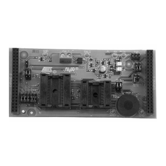
Introduction Section 1 Introduction The STK520 board is a top module designed to add AT90PWM family support to the STK500 development board from Atmel Corporation. The STK520 includes connectors and hardware allowing full utilization of the new fea- tures of the AT90PWM, while the Zero Insertion Force (ZIF) socket allows easy to use of SO24 &... - Page 4 Introduction Features STK520 is a New Member of the Successful STK500 Starter Kit Family. Supports the AT90PWM2 & AT90PWM3. DALI Hardware Interface. ® Supported by AVR Studio Zero Insertion Force Socket for SO24 & SO32 Packages. High Voltage Parallell Programming.
-
Page 5: Using The Stk520 Top Module
Using the STK520 Top Module Connecting the Connect the STK520 to the STK500 expansion header 0 and 1. It is important that the top module is connected in the correct orientation as shown in Figure 2-1. The STK520 to the... -
Page 6: Placing An At90Pwm2 On The Stk520
Figure 2-2. Pin1 on ZIF Socket PIN1 Caution: Do not mount an AT90PWM3 on the STK520 at the same time as an AVR is mounted on the STK500 board or at the same time as an AT90PWM2 is mounted on the STK520 board. - Page 7 Using the STK520 Top Module Caution: Do not mount an AT90PWM2 on the STK520 at the same time as an AVR is mounted on the STK500 board or at the same time as an AT90PWM3 is mounted on the STK520 board. None of the devices might work as intended.
-
Page 8: Programming The Avr
To program the AT90PWM3 using ISP Programming mode, connect the 6-wire cable between the ISP6PIN connector on the STK500 board and the ISP connector on the STK520 board as shown in Figure 2-4. The device can be programmed using the Serial Programming mode in the AVR Studio4 STK500 software. -
Page 9: High-Voltage Programming
Using the STK520 Top Module 2.2.2 High-voltage Figure 2-5. High-voltage (Parallel) Programming Programming To program the AVR using High-voltage (Parallel) Programming, connect the PROGC- TRL to PORTD and PROGDATA to PORTB on the STK500 as shown in Figure 2-5. Make sure that the TOSC-switch is placed in the XTAL position. -
Page 10: Jtagice Mkii Connector
This note explains which signals are required for ISP and which signals are required for debugWIRE. Figure 2-6 shows how to connect the JTAGICE mkII probe on the STK520 board. Figure 2-6. Connecting JTAG ICE to the STK520 The ISP connector is used for the AT90PWM3 built-in debugWire interface. The pin out of the connector is shown in Table 2-1 and is compliant with the pin out of the JTAG ICE available from Atmel. - Page 11 Using the STK520 Top Module Figure 2-7. JTAG Connector Table 2-1. STK520 ISP Connector Pinout Squid Squid Cable Target Target Cable Colours pins STK520 ISP pinout pins Colours grey MISO purple black MOSI green RESET brown STK520 User Guide 2-10...
-
Page 12: Stk520 Jumpers, Leds & Test Points
RX data detected by DALI Interface TX data sent to DALI Interface Table 2-4. STK520 Test Points Test Point Function Description Electrical ground of the STK520 board Electrical ground of the STK520 board AREF AREF pin of the AVR D2A output of the AVR DALI... -
Page 13: Dali Interface
Using the STK520 Top Module DALI Interface STK520 includes a non-isolated DALI Interface. The DALI Interface converts AVR RxD and TxD pin level to DALI compatible electrical level. It acts as a duplexer, so it inter- faces the two RxD and TxD lines to one DALI line. -
Page 14: Potentiometer
Using the STK520 Top Module Potentiometer The STK520 includes a potentiometer. To use the potentiometer, please mount JP13 and JP14 jumper. The potentiometer is supplied by AREF and it delivers a voltage to the AVR ADC0 input. Figure 2-10. Potentiometerr 2.6.0.1... -
Page 15: Troubleshooting Guide
RSTDISBL Fuse. Note: 1. See the application note “AVR065: LCD Driver for the STK520 LCD” on how to con- trol the LCD-display or the the application note “AVR064: STK520 – A Temperature Monitoring System with LCD Output”. -
Page 16: Technical Specifications
Maximum Input DALI Current ........500mA STK520 User Guide 4-16 7510A–AVR–08/05... -
Page 17: Technical Support
Technical Support Section 5 Technical Support For Technical support, please contact avr@atmel.com. When requesting technical sup- port, please include the following information: Which target AVR device is used (complete part number). Target voltage and speed. Clock source and fuse setting of the AVR. -
Page 18: Complete Schematics
Section 6 Complete Schematics On the following pages the complete schematics and assembly drawing of the STK520 revision A are shown. STK520 User Guide 6-18 Rev. 7510A–AVR–08/05... - Page 19 Complete Schematics Figure 6-1. Schematics, 1 of 4 6-19 STK520 User Guide 7510A–AVR–08/05...
- Page 20 Complete Schematics Figure 6-2. Schematics, 2 of 4 STK520 User Guide 6-20 7510A–AVR–08/05...
- Page 21 Complete Schematics Figure 6-3. Schematics, 3 of 4 6-21 STK520 User Guide 7510A–AVR–08/05...
- Page 22 Complete Schematics Figure 6-4. Schematics, 4 of 4 STK520 User Guide 6-22 7510A–AVR–08/05...
- Page 23 Complete Schematics Figure 6-5. Assembly Drawing, 1 of 1 JUMPER 6-23 STK520 User Guide 7510A–AVR–08/05...
- Page 24 Disclaimer: The information in this document is provided in connection with Atmel products. No license, express or implied, by estoppel or otherwise,to anyintellectu- alproperty right is granted by this document or in connection with the sale of Atmel products. EXCEPT AS SET FORTH IN ATMEL’S TERMS AND CONDI-TIONS OF SALE LOCATED ON ATMEL’S WEB SITE, ATMEL ASSUMES NO LIABILITY WHATSOEVER AND DISCLAIMS ANY EXPRESS, IMPLIED OR STATUTORYWAR-...
- Page 25 Mouser Electronics Authorized Distributor Click to View Pricing, Inventory, Delivery & Lifecycle Information: Microchip ATSTK520...
Need help?
Do you have a question about the STK520 and is the answer not in the manual?
Questions and answers