Table of Contents
Advertisement
User Manual
DA14531 Development Kit Pro
Hardware User Manual
UM-B-114
Abstract
Dialog Semiconductor's DA14531 development kit PRO consists of one DA145xx DEVKT-P PRO-
Motherboard, FCGQNFN daughterboard and a WLCSP daughterboard (the WLCSP daughterboard
must be purchased separately). This user manual describes the system functions of the hardware as
well as the guidelines of how to enable or disable features of the DA14531 development kit PRO.
Advertisement
Table of Contents

Related Manuals for Dialog Semiconductor DA14531 PRO


Summary of Contents for Dialog Semiconductor DA14531 PRO
-
Page 1: Abstract
Hardware User Manual UM-B-114 Abstract Dialog Semiconductor’s DA14531 development kit PRO consists of one DA145xx DEVKT-P PRO- Motherboard, FCGQNFN daughterboard and a WLCSP daughterboard (the WLCSP daughterboard must be purchased separately). This user manual describes the system functions of the hardware as... -
Page 2: Table Of Contents
How to Configure Power of DA14531 DK PRO ................. 36 Battery Operation ........................ 37 6.1.1 Enabling Coin Cell Battery on DA14531 PRO-DB ..........38 6.1.2 Enabling Coin Cell Battery on PRO-MB .............. 38 First Steps with DA14531 DK PRO .................... 40 Configuration of DA14531 DK PRO with a DA14531 FCGQFN24 PRO-DB ...... - Page 3 Appendix F Enabling UART, JTAG and 32.768 kHz Crystal ............75 UART (2-wire), JTAG, and 32.768 kHz Crystal ..............75 Full UART and JTAG ......................77 Revision History ..........................79 User Manual Revision 1.1 25-Oct-2019 CFR0012 3 of 80 © 2019 Dialog Semiconductor...
-
Page 4: Figures
Figure 31: BT1 Position (Left). Battery Holder, BC2032-F1, to Be Soldered (Right) ......38 Figure 32: DA14531 PRO-DB Schematic (Left). DA14531 PRO-MB, Header J4 Settings (Right) ..38 Figure 33: BT1 Position on PRO-MB (Left). Battery Holder, BU2032SM-BT-GTR, to Be Soldered (Right) .............................. -
Page 5: Tables
Figure 61: DA14531 PRO-MB, Current Measurement Circuit ............61 Figure 62: DA14531 PRO-MB, JTAG MCU ..................62 Figure 63: DA14531 PRO-MB, USB Hub, USB to UART IC, and Power Section ......63 Figure 64: Components on Top Side of DA14531 PRO-MB ............... 64 Figure 65: System Configuration for DA14531 DK PRO with a DA14531 WLCSP17 PRO-DB (Default) ............................... - Page 6 DA14531 Development Kit Pro Hardware User Manual Table 28: Pin Assignment for DA14531 FCGQFN24 PRO-DB ............77 Table 29: The Components for the Two Packages to Support Full UART and JTAG ......77 User Manual Revision 1.1 25-Oct-2019 CFR0012 6 of 80 © 2019 Dialog Semiconductor...
-
Page 7: Terms And Definitions
PRO daughterboard with DA14531 - FCGQFN24 WLCSP17 PRO-DB PRO daughterboard with DA14531 - WLCSP17 One-Time Programmable Memory References DA14531, Datasheet, Dialog Semiconductor. UM-B-083, SmartSnippets Toolbox User Manual, User Manual, Dialog Semiconductor. User Manual Revision 1.1 25-Oct-2019 CFR0012 7 of 80... -
Page 8: Introduction
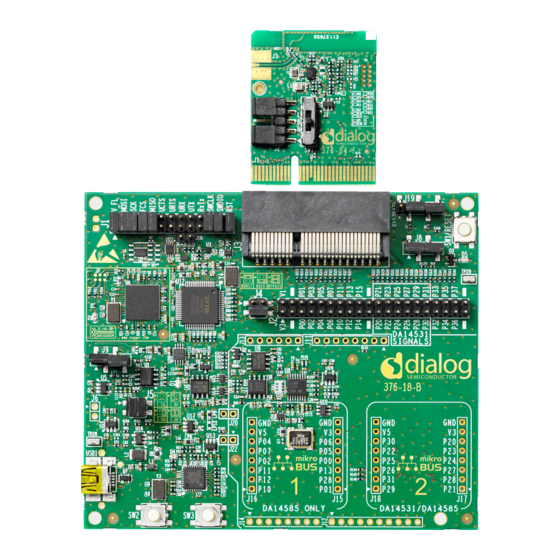
Table 1 present the part numbers (also ordering code) for the DK PRO DA14531-00FXDEVKT-P DK PRO PRO-MB 376-18-B Figure 1:DK PRO, DA14531-00FXDEVKT-P DK with PRO-MB and the PRO-DBs User Manual Revision 1.1 25-Oct-2019 CFR0012 8 of 80 © 2019 Dialog Semiconductor... -
Page 9: Table 1: Dk Pro Part Numbers And Description
The following sections guide users to understand the system setup, the different available configuration options, as well as the tools provided to debug, develop, and evaluate the system performance. User Manual Revision 1.1 25-Oct-2019 CFR0012 9 of 80 © 2019 Dialog Semiconductor... -
Page 10: System Overview
A slot to connect a DA14531 PRO-DB which hosts either the DA14531-FCGQFN24 or the DA14531-WLCSP17 SoC ● All the power wiring configurations to allow DA14531 PRO-MB to operate in either Buck, Boost, or Bypass mode ● Dedicated hardware for current measurement that enables Dialog’s SmartSnippets Toolbox... -
Page 11: Getting To Know Da14531 Dk Pro
DA14531 Development Kit Pro Hardware User Manual Getting to Know DA14531 DK PRO DA14531 PRO-DB The system on DA14531 PRO-DB consists of the DA14531 SoC, crystals, power section, and radio section. The system block diagram and the actual components location are presented in Figure 3,... -
Page 12: Figure 5: Da14531-00Ogdb-P, Wlcsp17 Pro-Db_[376-05-E]
R-Multiplexer: A group of 16 resistors of 0 Ω can be placed/removed as needed in order to hardwire various peripherals to the DA14531 pins as desired (Appendix To complete a configuration, it is necessary to set/remove jumpers on the DA14531 PRO-MB accordingly. The default settings are presented in section 5. User Manual Revision 1.1... -
Page 13: Power Section
DA14531 Development Kit Pro Hardware User Manual 4.1.1 Power Section The power circuit of DA14531 PRO-DB is designed to support two generations of PRO-MBs: ● PRO-MB: there is no need for the additional circuit. The DCDC power configuration and the voltage applied to DA14531 SoC are arranged on the PRO-MB (see section 6). -
Page 14: Figure 7: Power Section Of Da14531 Pro-Db
UM-B-114 DA14531 Development Kit Pro Hardware User Manual VBAT Figure 7: Power Section of DA14531 PRO-DB User Manual Revision 1.1 25-Oct-2019 CFR0012 14 of 80 © 2019 Dialog Semiconductor... -
Page 15: Rf Section
DA14531 Development Kit Pro Hardware User Manual 4.1.2 RF Section A printed F-antenna (ANT1) is used as the radiating element for the DA14531 PRO-DB. The DA14531 RFIO pin is connected to the printed antenna through a RF stripline and a matching circuit. -
Page 16: Pro-Mb (376-18-B)
Sense Circuit VLDO Selection ARDUINO J11, J12, J13, Connector USB1 KEYS MIKROBUS 1 USB HUB MIKROBUS 2 SW2 & SW3 J15, J16 J17, J18 Figure 11: PRO-MB (376-18-x) User Manual Revision 1.1 25-Oct-2019 CFR0012 16 of 80 © 2019 Dialog Semiconductor... - Page 17 J6: manual enable of USB hub voltage regulator. Not in use by default. ● J20: monitoring current sense circuit. Not mounted. No functional use. ● J22: it can provide 6.0 V to PRO-DB. Not mounted. No functional use. User Manual Revision 1.1 25-Oct-2019 CFR0012 17 of 80 © 2019 Dialog Semiconductor...
-
Page 18: Usb Hub (U11)
(LDOs and DCDC converter) for UART, JTAG, and the current sensing circuit. The system will power up only after the USB HUB has enumerated properly. Its operation is indicated via the green LED D4 on DA14531 PRO-MB. A 24 MHz crystal (Y3) is required for the chip operation. -
Page 19: Usb To Jtag (U4)
The USB to JTAG function is implemented by U4, SAM3U2CA. On the ROM of U4, software from SEGGER is loaded. Its operation is indicated via the green LED D2 on the DA14531 PRO-MB. This chip is supplied with 3.3 V from U14. U14 is enabled by the PWR_ENABLE signal. -
Page 20: Voltage Translator
U1A, where V3 (V ) is used as a reference. Consequently, there is DDIO BAT_HIGH no additional power consumption on the power circuitry of DA14531 PRO-MB due to voltage translation. Figure 15: Voltage Translator Circuitry of DA14531 PRO-MB User Manual Revision 1.1... -
Page 21: Power Section
U5, LDO. ● can be set to four different voltage levels. This is arranged by J5 settings. ● Generated power flows through the current sensing circuit to the DA14531 PRO-DB power supply pins: ○ V1 is connected to V BAT_LOW ○... -
Page 22: Gpios And Pin Assignment And Functions Of Da14531 Dk Pro
GPIOs and Pin Assignment and Functions of DA14531 DK PRO All signals of the DA14531 PRO-DBs are provided to DA14531 PRO-MB. The signal names are specific for the PRO-MB and do not have the same names as the signals of the PRO-DBs. The reason is that the PRO-MB can be used for both DA14531 SoC and DA1458x family of SoCs, whereas DA14531 SoC has fewer pins than DA1458x SoCs. -
Page 23: Figure 19: J1, Configuration Header On Da14531 Pro-Mb
DA14531 Development Kit Pro Hardware User Manual Figure 19: J1, Configuration Header on DA14531 PRO-MB The DA14531 PRO-DB GPIO pin assignment as well the configuration settings for the GPIOs of the PRO-MB are presented below. The DA14531 DK PRO signals connectivity is depicted in the... -
Page 24: Da14531 Wlcsp17 Pro-Db, Default Setup
● Please note that signals of DA14531 WLCSP17 PRO-DB are renamed on PRO-MB. The reason is that PRO-MB can be used for the PRO-DBs of DA1458x family User Manual Revision 1.1 25-Oct-2019 CFR0012 24 of 80 © 2019 Dialog Semiconductor... -
Page 25: Da14531 Fcgqfn24 Pro-Db, Default Setup
JTAG ○ SPI data flash ○ and single wire UART To enable these functions, apply the appropriate jumpers to the DA14531 PRO-MB ● Dual UART or full UART are not enabled. To enable UART, see section 5.3.4 ● Crystal 32.768 kHz is not enabled. For enabling crystal 32.768 kHz, refer to section ●... -
Page 26: Table 4: Da14531 Fcgqfn24 Pro-Db And Pro-Mb Signals Assignment (Default)
PWM_2 MBus2 J18:1 P0_9 J8:1-2 P1_0 J2_13 (Default) J1:23-24 P0_10 SW_DIO J1:24 SWDIO (Default) J19:2-3 P3_1 J2:31 INT_2 Arduino J14:2 (Default) P0_11 J8:3-4 P1_3 J2:16 C_TRIG (Default) User Manual Revision 1.1 25-Oct-2019 CFR0012 26 of 80 © 2019 Dialog Semiconductor... -
Page 27: Pro-Mb Setup
At power-on and before booting in the chip, reset is active high, and it is assigned to on P0_0. After booting, reset assignment and operation is handled by software. ● On a DA14531 PRO-DB, the reset signal provided by the PRO-MB is connected to P0_0 for WLCSP17 and FCGQFN24 through a 1 kΩ resistor ●... -
Page 28: Jtag
P0_2 SW_DIO J1:23-24 (Default) SWDIO P0_10 P0_5 JTAG signals are also available on DA14531 PRO-DBs on headerJ4 (Figure 22). Figure 22: Optional Debug Port 5.3.3 SPI Data Flash (U2) SPI data flash is enabled by default. The SPI data flash is the MX25R2035 from Macronix (2 Mbit) and located on DA14531 PRO-MB. -
Page 29: Uart
Any GPIO pin can be set as UART. In the DA14531 DK PRO, specific pins are used for UART signals (Table 7). Use short cables on DA14531 PRO-MB to bridge J2 pins (P2_0 to P3_1) and pins of J1 (odd pin-numbers). Table 7: UART Signals Assignment in DA14531 DK PRO... -
Page 30: Single-Wire Uart
● UTX and URX signals are multiplexed with FCS (chip select) and MISO of SPI data bus ● Two wires are required to connect UTX and URX to DA14531 PRO-DBs ● Disable SPI data flash by removing jumpers on J1 ●... -
Page 31: Full Uart (4-Wire) Configuration
UTX and URX as well as UCTS and URTS signals are multiplexed with FCS, MISO, MOSI, and SCK of the SPI data bus, respectively ● Four wires are required to connect UART signals to DA14531 PRO-DBs ● Disable SPI data flash by removing jumpers on J1 ●... -
Page 32: Push Buttons
Figure 26: Full UART (4-wire) Connectivity 5.3.5 Push Buttons ● There are two available push buttons, SW2 and SW3, on DA14531 PRO-MB ● Push buttons are available mainly for DA14531 FCGQFN24 PRO-DB ● SW3 is connected to SWDIO signal (P0_10 for DA14531 FCGQFN24). Users must enable SW3 on software ●... -
Page 33: User Led (D5) And C-Trig (Software Cursor)
WLCSP17 J8:1-2 (Default) P1_0 P0_9 Also assigned to SW2. In order not to disturb C- C_TRIG J8:3-4 (Default) P1_3 P0_11 TRIG operation, remove the jumper from J18:2-3. User Manual Revision 1.1 25-Oct-2019 CFR0012 33 of 80 © 2019 Dialog Semiconductor... -
Page 34: Mikrobus 2 Interface
DA14531 Development Kit Pro Hardware User Manual 5.3.7 mikroBUS 2 Interface ● mikroBUS 2 is used for DA14531 PRO-DB ● Two female headers (8 position 0.100", through hole, socket type) must be mounted on J17 and ● DA14531 FCGQFN24 PRO-DB is suitable for mikroBUS operation due to its available pins ●... -
Page 35: Arduino Interface
It is not enabled. INT_2 J14-2 P3_1 P0_11 The same voltage rail applied to J11:4 BAT_HIGH pin of DA14531 SoC. BAT_HIGH VBUS_HUB voltage provided from J11:5 USB port. User Manual Revision 1.1 25-Oct-2019 CFR0012 35 of 80 © 2019 Dialog Semiconductor... -
Page 36: How To Configure Power Of Da14531 Dk Pro
Table 16. Jumpers are applied by default. On DA14531 PRO DBs (WLCSP17 and FCGQFN24), users must set SW1 to buck position permanently. The power circuit consisting of U2 and SW1 on PRO-DBs is not needed. Figure 30: DA14531 PRO-DB Configuration and DA14531 PRO-MB Jumpers User Manual Revision 1.1... -
Page 37: Battery Operation
Example: to provide 3.0 V in buck mode, proceed with the following actions: 1. On DA14531 PRO-MB, apply jumpers to J5:2-4 and J4:3-4. 2. On DA14531 PRO-DB, set SW1 to the H position (buck mode) and apply jumpers to J1:1-2 and J1:4-5... -
Page 38: Enabling Coin Cell Battery On Da14531 Pro-Db
Figure 32: DA14531 PRO-DB Schematic (Left). DA14531 PRO-MB, Header J4 Settings (Right) 6.1.1 Enabling Coin Cell Battery on DA14531 PRO-DB To enable a coin cell battery on DA14531 PRO-DB, before powering on the DA14531 DK PRO, make the following changes: ●... -
Page 39: Figure 33: Bt1 Position On Pro-Mb (Left). Battery Holder, Bu2032Sm-Bt-Gtr, To Be Soldered (Right)
Solder the battery socket on the solder side (BT1) by using BU2032SM-BT-GTR (see Figure ○ Insert a CR2032 coin cell battery Figure 33: BT1 Position on PRO-MB (Left). Battery Holder, BU2032SM-BT-GTR, to Be Soldered (Right) User Manual Revision 1.1 25-Oct-2019 CFR0012 39 of 80 © 2019 Dialog Semiconductor... -
Page 40: First Steps With Da14531 Dk Pro
In the following sections, the supported features are detailed for each daughterboard. Configuration of DA14531 DK PRO with a DA14531 FCGQFN24 PRO-DB Figure 34: Default Setup of the DA14531 DK PRO with DA14531 FCGQFN24 PRO-DB User Manual Revision 1.1 25-Oct-2019 CFR0012 40 of 80 © 2019 Dialog Semiconductor... - Page 41 In the DA14531 FCGQFN24 PRO-DB, the push button SW1 must be placed in the H position for BUCK mode (Figure 34). The DA14531 PRO-MB is delivered in a default configuration (Figure 34) which: ● Enables the on-board SPI data flash ●...
-
Page 42: Configuration Of Da14531 Dk Pro With A Da14531 Wlcsp17 Pro-Db
In the DA14531 WLCSP17 PRO-DB, the push button SW1 must be placed in the H position for BUCK mode (Figure 35). The DA14531 PRO-MB is delivered in a default configuration (Figure 35) which: ● Enables the on-board SPI data flash ●... -
Page 43: Current Measurements
DA14531 Development Kit Pro Hardware User Manual Current Measurements Current drawn from the DA14531 PRO-DB can be measured with a good accuracy by using the current sensing circuit and the power profiler of Dialog’s SmartSnippets Toolbox. In this section, the current measurement circuit as well as the setup and the measurements of the power profiler are described, and the measurement accuracy is presented. -
Page 44: Power Profiler Of Smartsnippet Toolbox
JTAG is used for downloading code from the IDE and debugging. The “Hybrid” option can also be used. But power measurements are not feasible in the “UART-only” or “JTAG” option. User Manual Revision 1.1 25-Oct-2019 CFR0012 44 of 80 © 2019 Dialog Semiconductor... -
Page 45: Power Profiler Setup
Power Profiler application in SmartSnippets Toolbox will pop up (Figure 40). Press “Config” button in the bottom right and check if everything is configured correctly (Figure 41). User Manual Revision 1.1 25-Oct-2019 CFR0012 45 of 80 © 2019 Dialog Semiconductor... -
Page 46: Figure 40: Power Profiler Of Smartsnippets Toolbox Main Window
42) and set the max scale of “Current1” to 10 mA. Note that this does not affect in any way the accuracy of measurement. It only zooms-in the waveform that is presented on the viewer window. User Manual Revision 1.1 25-Oct-2019 CFR0012 46 of 80 © 2019 Dialog Semiconductor... -
Page 47: Measurements
A/D converter) and then press “Start”. Figure 43: Free Running Capture A triggered capture can be used for acquiring a single waveform (Figure 44). User Manual Revision 1.1 25-Oct-2019 CFR0012 47 of 80 © 2019 Dialog Semiconductor... -
Page 48: Figure 44: Triggered Capture
Note that the “Auto Trigger” and “Auto Stop” checkboxes under “Control” on the lower right-hand side must remain unchecked. Figure 45: Oscilloscope Option User Manual Revision 1.1 25-Oct-2019 CFR0012 48 of 80 © 2019 Dialog Semiconductor... -
Page 49: Power Profiler Software Cursors
2. In the main window of the Power Profiler, press “Config” and temporarily set the calibration offset to zero (Figure 47). Figure 47: Setting Offset to Zero User Manual Revision 1.1 25-Oct-2019 CFR0012 49 of 80 © 2019 Dialog Semiconductor... -
Page 50: Figure 48: Measuring Offset
NOTE Please notice that the value in the Voltage box is 3 V. This is a typical value used across the industry for comparing BLE power measurements. Therefore, the power configuration on DA14531 PRO-MB must be updated accordingly (J5: 2-4). -
Page 51: Accuracy Of Current Measurement Circuit
DA14531 Development Kit Pro Hardware User Manual Accuracy of Current Measurement Circuit The measuring range of the current measurement circuit in DA14531 PRO-MB is 1 μΑ to 240 mA. The circuit accuracy is measured by applying a constant current, monitoring the output with the SmartSnippets Toolbox, and compare the outcome. -
Page 52: Figure 51: Current Measurement Circuit Inaccuracy, Indicative Graph
DA14531 Development Kit Pro Hardware User Manual 1.1V boost 1.8V buck 3.3V buck 1.E-06 1.E-05 1.E-04 1.E-03 1.E-02 1.E-01 input current (A) Figure 51: Current Measurement Circuit Inaccuracy, Indicative Graph User Manual Revision 1.1 25-Oct-2019 CFR0012 52 of 80 © 2019 Dialog Semiconductor... -
Page 53: Known Issues
SW3 is enabled on DA145xx DEVKT-P PRO-MB by P1_1. By default, this signal is not driven from DA14531. Consequently, jumper J19:4-5 is not required in DA14531 DK PRO. Figure 53: Disable SW3. Remove Jumper from J19:4-5 User Manual Revision 1.1 25-Oct-2019 CFR0012 53 of 80 © 2019 Dialog Semiconductor... -
Page 54: Mikrobus Wrong Label
Figure 54: mikroBUS Wrong Label 4-Wire UART Special Considerations When the 4-wire UART functionality is used with DA14531 Pro-DB and the reset function is enabled on P0_0, the chip will not boot and still remain in the reset state. Figure 55: Full UART Configuration - CTS Issue User Manual Revision 1.1... - Page 55 As shown in Figure 55, the UCTS signal is shorted to P0_0 when a DA14531 PRO-DB is used. This has been done to maintain compatibility with DA14585 daughterboards. The UCTS signal is an input to the DA14531 and is driven high from the motherboard side (MB_RTS). If P0_0 is configured as reset (active high), the motherboard will keep the DA14531 in reset indefinitely and prevent it from booting (the Booter defaults this pin to the reset function between boot steps).
-
Page 56: Appendix A Fcgqfn24 Pro-Db: Da14531-00Fxdb-P_(376-04-F2)
UM-B-114 DA14531 Development Kit Pro Hardware User Manual Appendix A FCGQFN24 PRO-DB: DA14531-00FXDB-P_(376-04-F2) Schematic Figure 56: Schematic, FCGQFN24, DA14531-00FXDB-P_(376-04-F2) User Manual Revision 1.1 25-Oct-2019 CFR0012 56 of 80 © 2019 Dialog Semiconductor... -
Page 57: Components Placement
UM-B-114 DA14531 Development Kit Pro Hardware User Manual Components Placement Figure 57: Components on Top and Bottom Sides for FCGQFN24, DA14531-00FXDB-P_(376- 04-F2) User Manual Revision 1.1 25-Oct-2019 CFR0012 57 of 80 © 2019 Dialog Semiconductor... -
Page 58: Appendix B Wlcsp17 Pro-Db: Da14531-00Ogdb-P_(376-05-E)
UM-B-114 DA14531 Development Kit Pro Hardware User Manual Appendix B WLCSP17 PRO-DB: DA14531-00OGDB-P_(376-05-E) Schematic Figure 58: Schematic, WLCSP17, DA14531-00OGDB-P_(376-05-E) User Manual Revision 1.1 25-Oct-2019 CFR0012 58 of 80 © 2019 Dialog Semiconductor... -
Page 59: Components Placement
UM-B-114 DA14531 Development Kit Pro Hardware User Manual Components Placement Figure 59: Components on Top and Bottom Sides for WLCSP17, DA14531-00OGDB-P_(376-05- User Manual Revision 1.1 25-Oct-2019 CFR0012 59 of 80 © 2019 Dialog Semiconductor... -
Page 60: Appendix C Pro-Mb
UM-B-114 DA14531 Development Kit Pro Hardware User Manual Appendix C PRO-MB Schematic Figure 60: DA14531 PRO-MB, headers and connectors User Manual Revision 1.1 25-Oct-2019 CFR0012 60 of 80 © 2019 Dialog Semiconductor... -
Page 61: Figure 61: Da14531 Pro-Mb, Current Measurement Circuit
UM-B-114 DA14531 Development Kit Pro Hardware User Manual Figure 61: DA14531 PRO-MB, Current Measurement Circuit User Manual Revision 1.1 25-Oct-2019 CFR0012 61 of 80 © 2019 Dialog Semiconductor... -
Page 62: Figure 62: Da14531 Pro-Mb, Jtag Mcu
UM-B-114 DA14531 Development Kit Pro Hardware User Manual Figure 62: DA14531 PRO-MB, JTAG MCU User Manual Revision 1.1 25-Oct-2019 CFR0012 62 of 80 © 2019 Dialog Semiconductor... -
Page 63: Figure 63: Da14531 Pro-Mb, Usb Hub, Usb To Uart Ic, And Power Section
UM-B-114 DA14531 Development Kit Pro Hardware User Manual Figure 63: DA14531 PRO-MB, USB Hub, USB to UART IC, and Power Section User Manual Revision 1.1 25-Oct-2019 CFR0012 63 of 80 © 2019 Dialog Semiconductor... -
Page 64: Components Placement
UM-B-114 DA14531 Development Kit Pro Hardware User Manual Components Placement Figure 64: Components on Top Side of DA14531 PRO-MB User Manual Revision 1.1 25-Oct-2019 CFR0012 64 of 80 © 2019 Dialog Semiconductor... -
Page 65: Appendix D Detailed Description Of Hardware Setup
R15 = 36 Signals Naming MB0_4 R28 = NP On PRO-Motherboard MB0_5 R29 = NP Figure 65: System Configuration for DA14531 DK PRO with a DA14531 WLCSP17 PRO-DB (Default) User Manual Revision 1.1 25-Oct-2019 CFR0012 65 of 80 © 2019 Dialog Semiconductor... -
Page 66: Da14531 Fcgqfn24 Pro-Db, Gpios Configuration, And R-Matrix
The default setup for the D14531 FCGQFN24 PRO-DB is: Reset, JTAG, and SPI data bus (assigned to SPI data flash), single-wire UART, LED and a Key. Extension ports use multiplexed signals. Figure 66 Table 19 show the resistor matrix for FCGQFN24. User Manual Revision 1.1 25-Oct-2019 CFR0012 66 of 80 © 2019 Dialog Semiconductor... -
Page 67: Figure 66: System Configuration For Da14531 Dk Pro With A Da14531 Fcgqfn24 Pro-Db (Default)
R11 = NP P3_0 P0_10 P1_3 R18 = 1K MB3_1 R12 = 36 P0_11 P3_1 Figure 66: System Configuration for DA14531 DK PRO with a DA14531 FCGQFN24 PRO-DB (Default) User Manual Revision 1.1 25-Oct-2019 CFR0012 67 of 80 © 2019 Dialog Semiconductor... -
Page 68: Table 19: Da4531 Fcgqfn24 Pro-Db Default Setup
P2_5 PRO-MB signals P2_6 P2_7 P2_8 P2_9 P3_0 P3_1 UART URTS UCTS MOSI MISO SPI Data Flash SWCLK JTAG SWDIO XT32Kp XTAL32K XT32K RESET BUTTO Other SW_TRI User Manual Revision 1.1 25-Oct-2019 CFR0012 68 of 80 © 2019 Dialog Semiconductor... -
Page 69: Appendix E Spi Data Flash, Jtag, And Single-Wire Uart (Default)
R6 = Not pop MB2_5 P2_5 P0_5 SWDIO SWDIO R15 = 36 Signals Naming On PRO-Motherboard Figure 67: System Configuration for DA14531 DK PRO with a DA14531 WLCSP17 PRO-DB (Default) User Manual Revision 1.0 25-Oct-2019 CFR0012 69 of 80 © 2019 Dialog Semiconductor... -
Page 70: Figure 68: Jumper Settings For Pro-Mb (Marked In Red)
R6, R23, R24, R25, R26, R27, R28, R29, R33, R34, R35, Y2 R14, R15, R19, R20, R21, R22, R30 Figure 68: Jumper Settings for PRO-MB (Marked in Red) User Manual Revision 1.0 25-Oct-2019 CFR0012 70 of 80 © 2019 Dialog Semiconductor... -
Page 71: Da14531 Fcgqfn24 Pro-Db And Pro-Mb Settings
DA14531 DK PRO, three additional jumpers need to be added (marked in blue in Figure 71): J1:19-20, J10:1 to J1:15, and J10:2 to J1:17. The resistors that are not mounted to FCGQFN24 PRO-DB do not appear in Figure 70 User Manual Revision 1.0 25-Oct-2019 CFR0012 71 of 80 © 2019 Dialog Semiconductor... -
Page 72: Figure 70: System Configuration For Da14531 Dk Pro With A Da14531 Fcgqfn24 Pro-Db (Default)
R18 = 1K MB3_1 R12 = 36 Signals Naming P0_11 P3_1 On PRO-MB Figure 70: System Configuration for DA14531 DK PRO with a DA14531 FCGQFN24 PRO-DB (Default) User Manual Revision 1.0 25-Oct-2019 CFR0012 72 of 80 © 2019 Dialog Semiconductor... -
Page 73: Figure 71: Jumper Settings For Pro-Mb
R8, R9, R10, R12, R14, R16, R17, R26, R27, R28, R29, R33, R34, R18, R35, Y2 R19, R20, R21, R22, R30, R31 Figure 71: Jumper Settings for PRO-MB User Manual Revision 1.0 25-Oct-2019 CFR0012 73 of 80 © 2019 Dialog Semiconductor... -
Page 74: Figure 72: Resistor And Jumper Settings For Da14531 Fcgqfn24 Pro-Db
UM-B-114 DA14531 Development Kit Pro Hardware User Manual Figure 72: Resistor and Jumper Settings for DA14531 FCGQFN24 PRO-DB User Manual Revision 1.0 25-Oct-2019 CFR0012 74 of 80 © 2019 Dialog Semiconductor... -
Page 75: Appendix F Enabling Uart, Jtag And 32.768 Khz Crystal
R1, R2, R3, R6, R7, R8, R9, R10, R4, R5, R11, R13, R15, R19, R20, DA14531-FCGQFN24 R12, R14, R16, R17, R18, R23, R21, R22, R25, R26, R27, R28, R29 R24, R30, R31, Y2 User Manual Revision 1.0 25-Oct-2019 CFR0012 75 of 80 © 2019 Dialog Semiconductor... -
Page 76: Figure 73: Resistor And Jumper Setting For Pro-Mb (Top) And Da14531 Pro-Dbs (Bottom) To
DA14531 Development Kit Pro Hardware User Manual PRO-MB Jumpers (in Red) WLCSP17 FCGQFN24 Figure 73: Resistor and Jumper Setting for PRO-MB (Top) and DA14531 PRO-DBs (Bottom) to Support 2-Wire UART, JTAG, and 32.768 kHz Crystal User Manual Revision 1.0 25-Oct-2019... -
Page 77: Full Uart And Jtag
R11, R13, R15, R19, R20, R21, DA14531 FCGQFN24 PRO-DB R8, R9, R10, R12, R14, R16, R17, R22, R27, R28, R29, R33, R34, R18, R23, R24, R25, R26, R30, R35, Y2 User Manual Revision 1.0 25-Oct-2019 CFR0012 77 of 80 © 2019 Dialog Semiconductor... -
Page 78: Support Full Uart And Jtag
UM-B-114 DA14531 Development Kit Pro Hardware User Manual PRO MB jumpers (in red) WLCSP17 FCGQFN24 Figure 74: Resistor and Jumper Setting for PRO-MB (Top) and DA14531 PRO-DBs (Bottom) to Support Full UART AND JTAG User Manual Revision 1.0 25-Oct-2019 CFR0012 78 of 80 ©... -
Page 79: Revision History
UM-B-114 DA14531 Development Kit Pro Hardware User Manual Revision History Revision Date Description 24-Oct-2019 Editorial review. 15-Oct-2019 Initial version. User Manual Revision 1.0 25-Oct-2019 CFR0012 79 of 80 © 2019 Dialog Semiconductor... -
Page 80: Um-B
Dialog Semiconductor product (or associated software) can reasonably be expected to result in personal injury, death or severe property or environmental damage.
Need help?
Do you have a question about the DA14531 PRO and is the answer not in the manual?
Questions and answers