
Subscribe to Our Youtube Channel
Related Manuals for Dialog Semiconductor DA1469 PRO series


Summary of Contents for Dialog Semiconductor DA1469 PRO series
-
Page 1: Abstract
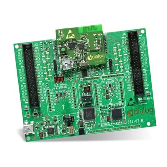
User Manual DA1469x PRO Development Kit UM-B-093 Abstract DA1469x Development Kit Pro hardware provides a tested reference platform, access to all signals for connecting peripherals, and advanced debugging features. -
Page 2: Table Of Contents
Figure 18: Negative Supply for Op-Amps .................... 14 Figure 19: Voltage Level Translation Circuit ..................15 Figure 20: Mainboard/Daughterboard Alignment ................16 Figure 21: QSPI-RAM .......................... 18 User Manual Revision 1.1 19-Feb-2019 CFR0012 2 of 22 © 2019 Dialog Semiconductor... -
Page 3: Tables
Table 4: Default Jumper Settings ......................18 Table 5: Mainboard Test Points (Placed on the Bottom Of DA1469x PRO DK) ......... 18 Table 6: Daughterboard Test Points ....................20 User Manual Revision 1.1 19-Feb-2019 CFR0012 3 of 22 © 2019 Dialog Semiconductor... -
Page 4: Terms And Definitions
DA1469x, Datasheet, Dialog Semiconductor. AN-B-052, DA1458x/68x Development Kit J-Link Interface, Application Note, Dialog Semiconductor. AN-B-037, DA1468x Power Measurements, Application Note, Dialog Semiconductor. DA1469x Pro Development Kit Mainboard Schematics, Reference Design, Dialog Semiconductor. DA1469x Pro Development Kit VFBGA-100 Schematics, Reference Design, Dialog Semiconductor. -
Page 5: Da1469X Dk Pro Hardware Architecture And Implementation
Look and feel similar to DA14680 PRO DK ■ DA1469x silicon easily replaceable on a daughterboard core module 3.3 DA1469x PRO DK Hardware Block Diagram Figure 1: System Block Diagram User Manual Revision 1.1 19-Feb-2019 CFR0012 5 of 22 © 2019 Dialog Semiconductor... -
Page 6: Main Features Of Mainboard In Da1469X Pro Dk
12.0k 10nF 1.0uF 1.0uF SHDN TP11 R121 AP2127K-ADJTRG1 9.53k 3.9k 87898-0455 8.06k PWR_ENABLE R127 100.0k 3.0V PLACE 2-3 PLACE 1-2 1.8V OPEN Figure 3: VBAT Adjustable LDO User Manual Revision 1.1 19-Feb-2019 CFR0012 6 of 22 © 2019 Dialog Semiconductor... -
Page 7: Figure 4: Dip Switch
Optional Arduino sockets (supporting 3.3 V compatible Arduino shields) Figure 5: Arduino Sockets ■ Optional 2× MikroBUS sockets (supporting 3.3 V compatible click boards from MikroElektronika or other sources) Figure 6: MikroBUS sockets User Manual Revision 1.1 19-Feb-2019 CFR0012 7 of 22 © 2019 Dialog Semiconductor... -
Page 8: User Accessible Elements In Da1469X Pro Dk
12. Trimmer to define the adjustable LDO voltage (R127) 13. User button (K1) 14. RF coaxial switch (J7 on daughterboard) 15. Signal/Power breakout headers (J3 and J4) 16. LRA/ERM interface header (J10) User Manual Revision 1.1 19-Feb-2019 CFR0012 8 of 22 © 2019 Dialog Semiconductor... -
Page 9: Da1469X Pro Dk Daughterboard (Db-Vfbga-100 And Db-Lfbga-86)
OVP circuit on the VBUS power input (Figure VBUS VBUS_IN DMP3099L-7 100nF 2.2k BC807-25_215 R23 4.7k BZX84C5V6-7-F 10.0k DIODES Inc. Figure 9: USB Overvoltage Protection ● Battery/Power connectors (Figure 10): User Manual Revision 1.1 19-Feb-2019 CFR0012 9 of 22 © 2019 Dialog Semiconductor... -
Page 10: Figure 10: Power Options
○ SWD pins connected to Cortex M33 core ○ Reset from JLink-OB or button on the CIB board ○ 2-pin UART signals connected to bootable UART pins User Manual Revision 1.1 19-Feb-2019 CFR0012 10 of 22 © 2019 Dialog Semiconductor... -
Page 11: Figure 12: Cib Debugging Header
ESD protection diodes at the most susceptible points (USB connector J3, CIB interface J4, and power selector switch SW1) ● Possibility to operate stand-alone (without the mainboard), powered from one of these options: User Manual Revision 1.1 19-Feb-2019 CFR0012 11 of 22 © 2019 Dialog Semiconductor... -
Page 12: Current Measurement Section In Da1469X Dk Pro
The debugging section consists of JTAG, UART, and current sense circuitry. This section is supplied from the mainboard USB connector. The USB Hub has its own dedicated 3.3 V LDO (U13, always on, Figure 15). User Manual Revision 1.1 19-Feb-2019 CFR0012 12 of 22 © 2019 Dialog Semiconductor... -
Page 13: Figure 15: 3.3V Ldo For Usb Hub
LP13 TP39 5.0V 500mA_470 OHM 1.0uF 1.0uF 4.7uF 1.0nF MIC5205-5.0Y M5 AP3012KTR-G1 R83 38.3k PWR_ENABLE SHDN 10.0k 1.0uF C105 100nF Figure 17: Op-Amps/ADC 5.0 V Power Supply User Manual Revision 1.1 19-Feb-2019 CFR0012 13 of 22 © 2019 Dialog Semiconductor... -
Page 14: Figure 18: Negative Supply For Op-Amps
JTAG/UART) is fixed at 3.3 V, there is a leakage through the pins if the DA1469x voltage I/Os are at 3.0 V or less. Table 1: Signals with Level Translation Pin Name Signal Name P0_10 SWDIO P0_11 SWCLK P0_9 P0_8 P1_0 URTS P0_7 UCTS User Manual Revision 1.1 19-Feb-2019 CFR0012 14 of 22 © 2019 Dialog Semiconductor... -
Page 15: Figure 19: Voltage Level Translation Circuit
180°. Small arrows on the top silk screens of both boards are added to indicate a properly aligned placement (Figure 20). The arrows on the mainboard must point to the arrows on the daughterboard. User Manual Revision 1.1 19-Feb-2019 CFR0012 15 of 22 © 2019 Dialog Semiconductor... -
Page 16: Gpio Assignments
P0_12 P0_13 P0_14 USB_DP Daughterboard USB P0_15 USB_DM P0_16 C_TRIG software trigger P0_17 P0_18 P0_19 P0_20 P0_21 P0_22 XTAL32km Daughterboard xtal 32.768kHz P0_23 XTAL32kp P0_24 P0_25 P0_26 User Manual Revision 1.1 19-Feb-2019 CFR0012 16 of 22 © 2019 Dialog Semiconductor... - Page 17 LCD (various types), micro-motor drive, ADC inputs, NTC (charger), and sleep mode PWM outputs are available on specific pins only. Check the DA1469x datasheet for more details. User Manual Revision 1.1 19-Feb-2019 CFR0012 17 of 22 © 2019 Dialog Semiconductor...
-
Page 18: Jumper/Dip Switch Settings
Table 5: Mainboard Test Points (Placed on the Bottom Of DA1469x PRO DK) TP Name on Reference Signal Name Comments Design VDD_CR 3.3V (SEGGER) T_RESET JTAG Reset sERASE SEGGER chip programming sVCC sRST sDIO sCLK sTDI DBLED SEGGER LED User Manual Revision 1.1 19-Feb-2019 CFR0012 18 of 22 © 2019 Dialog Semiconductor... -
Page 19: Um-B
TP48 UART Tx (FTDI side) TP49 SWDIO SEGGER data I/O TP50 UART Rx (FTDI side) TP51 URTS UART RTS (FTDI side) TP52 UCTS UART CTS (FTDI side) User Manual Revision 1.1 19-Feb-2019 CFR0012 19 of 22 © 2019 Dialog Semiconductor... -
Page 20: Table 6: Daughterboard Test Points
5.0 V ± 5% (to DA1469x pin) bottom TP18 VLED LED power (VBUS or VBAT - 0.2 V) bottom TP20 TP21 VFLASH 1.8 V ± 5% bottom User Manual Revision 1.1 19-Feb-2019 CFR0012 20 of 22 © 2019 Dialog Semiconductor... -
Page 21: Revision History
● Update document title to “DA1469x PRO Development Kit” ● Removed reference to Basic Kit ● Minor text editing ● Improved template compliance 15-Feb-2018 Initial version (specification) User Manual Revision 1.1 19-Feb-2019 CFR0012 21 of 22 © 2019 Dialog Semiconductor... - Page 22 Terms and Conditions of Sale, available on the company website (www.dialog-semiconductor.com) unless otherwise stated. Dialog and the Dialog logo are trademarks of Dialog Semiconductor plc or its subsidiaries. All other product or service names are the property of their respective owners.
Need help?
Do you have a question about the DA1469 PRO series and is the answer not in the manual?
Questions and answers