Table of Contents
Advertisement
Quick Links
Advertisement
Table of Contents

Related Manuals for Acces I/O products PCIe-DIO-24S


Summary of Contents for Acces I/O products PCIe-DIO-24S
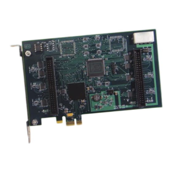
- Page 1 10623 Roselle Street, San Diego, CA 92121 (858) 550-9559 Fax (858) 550-7322 contactus@accesio.com www.accesio.com MODELS PCIe-DIO-48S PCIe-DIO-48 PCIe-DIO-24S PCI Express 48 Channel Digital I/O Card with Change of State Detection USER MANUAL File: MPCIe-DIO-48S.B1b...
- Page 2 ACCES, nor the rights of others. IBM PC, PC/XT, and PC/AT are registered trademarks of the International Business Machines Corporation. Printed in USA. Copyright 2009 by ACCES I/O Products, Inc. 10623 Roselle Street, San Diego, CA 92121. All rights reserved.
- Page 3 Warranty Prior to shipment, ACCES equipment is thoroughly inspected and tested to applicable specifications. However, should equipment failure occur, ACCES assures its customers that prompt service and support will be available. All equipment originally manufactured by ACCES which is found to be defective will be repaired or replaced subject to the following considerations.
-
Page 4: Table Of Contents
TABLE OF CONTENTS Chapter 1: Introduction............................5 Features ................................5 Applications............................... 5 Functional Description ............................. 5 Ordering Guide..............................7 Factory Options..............................7 Optional Accessories ............................7 Chapter 2: Installation............................8 Software CD Installation........................... 8 Hardware Installation............................8 Chapter 3: Hardware Details..........................9 Option Selection.............................. -
Page 5: Chapter 1: Introduction
Chapter 1: Introduction The PCIe-DIO-48(S) is a x1 lane PCI Express (PCIe) board designed for use in a variety of Digital I/O (DIO) applications. It uses the high speed PCIe bus to transfer digital data to and from the board. The DIO emulates 8255 compatible chips making it easy program. -
Page 6: Figure 1-1: Block Diagram
When a port has COS enabled, any changes of the port's bits (low-to-high or high-to-low) will cause an interrupt. Refer to Chapter 5: Programming for enabling, disabling, and clearing the interrupts. Each DIO line is buffered and capable of sourcing 32mA or sinking 64mA. The VCCIO level is 5V or can be factory configured as 3.3V. -
Page 7: Ordering Guide
PCIe-DIO-48S 48-bit Digital I/O card with change of state detection • PCIe-DIO-48 48-bit Digital I/O card • PCIe-DIO-24S 24-bit Digital I/O card with change of state detection Factory Options • Extended temperature operation (-40° to +85°C) • Molex PC-style connector for maximum 5V VCCIO current sourcing capability •... -
Page 8: Chapter 2: Installation
Chapter 2: Installation Software CD Installation The software provided with this board is contained on one CD and must be installed onto your hard disk prior to use. To do this, perform the following steps as appropriate for your operating system. Substitute the appropriate drive letter for your drive where you see D: in the examples below. -
Page 9: Chapter 3: Hardware Details
Chapter 3: Hardware Details Option Selection Refer to the setup program on the CD provided with the board. Also, refer to the Block Diagram and the Option Selection Map when reading this section of the manual. C3 IRQ Enable To enable the C3 IRQ, install the IEN jumper in the "EN" position followed by a read/write access to Base Address + B (Refer to Chapter 5: Programming for details). -
Page 10: Vccio Resettable Fused Outputs
VCCIO Resettable Fused Outputs There are two 0.5A resettable fuses. Each fuse feeds one I/O connector at pin 49 used to power external module racks, relay boards, or for general purposes. If an over-current persists on a circuit protected by the resettable fuse, it will open interrupting power to the circuit. The amount of time it takes the fuse to act depends on the amount of over-current and other conditions such as ambient temperature, humidity, etc. -
Page 11: Chapter 4: Address Selection
The Device ID for the PCIe-DIO-48S is 0x0E61. The Device ID for the PCIe-DIO-48 is 0x0C61. The Device ID for the PCIe-DIO-24S is 0x0E53. This card uses I/O addresses offset from the base address assigned by the PCIe bus. The address spaces are defined in the programming section of this manual. -
Page 12: Chapter 5: Programming
Chapter 5: Programming This card is an I/O-mapped device that is easily configured from any language. The base address is assigned by the computer system during installation. The card's read/write functions are as follows. Address Function Operation Base Address +0 PA Group 0 Read/Write Base Address +1... -
Page 13: Table 5-3: Base +1 Group 0, Port B Dio; Base +5 Group 1, Port B Dio
Base Address +1 (read/write) Group 0, Port B DIO; +5 (read/write) Group 1, Port B DIO Bit 7 Bit 6 Bit 5 Bit 4 Bit 3 Bit 2 Bit 1 Bit 0 Table 5-3: Base +1 Group 0, Port B DIO; Base +5 Group 1, Port B DIO Reading from this address will return the digital data on Port B. -
Page 14: Table 5-6: Base +B, Cos/C3 Irq Enable
Base Address +B (read/write) COS/C3 IRQ Enable Bit 7 Bit 6 Bit 5 Bit 4 Bit 3 Bit 2 Bit 1 Bit 0 Group 1 Group 1 Group 1 Group 0 Group 0 Group 0 ‘0’ ‘0’ Port C Port B Port A Port C Port B... -
Page 15: Chapter 6: Connector Pin Assignments
Chapter 6: Connector Pin Assignments Two 50-pin male headers are provided for I/O connections designated as P2 and P3, corresponding to Group 0 and Group 1 respectively. The mating connector is an AMP type 1-746285-0 or equivalent Figure 6-1: 50-Pin Male Header Pin Signal Name Pin Signal Name PC3* VCCIO... -
Page 16: Table 6-2: I/O Header Connector Signal Names, Directions And Descriptions
Signal Name I/O Signal Description Name I/O Port C bit 7 I/O Port C bit 6 I/O Port C bit 5 I/O Port C bit 4 I/O Port C bit 3 / when C3 IRQ is enabled will generate an IRQ on a rising edge I/O Port C bit 2 I/O Port C bit 1 I/O Port C bit 0... -
Page 17: Chapter 7: Specifications
Chapter 7: Specifications VCCIO 5V or optionally 3.3V Digital Inputs Logic High 2.0V to VCCIO Logic Low 0V to 0.8V Current ±20uA (max) Digital Outputs Logic High 2.0V (min); 32mA source Logic Low 0.55V (max); 64mA sink Power Output VCCIO (P2 & P3; pin 49) Environmental Operating Temperature 0°... -
Page 18: Customer Comments
Customer Comments If you experience any problems with this manual or just want to give us some feedback, please email us at: manuals@accesio.com. Please detail any errors you find and include your mailing address so that we can send you any manual updates. 10623 Roselle Street, San Diego CA 92121 Tel. - Page 19 Partner in Electronic Components & Supply Chain Solutions The Netherlands Denmark Elektrostraat 17 Fuglegaardsvaenget 25 NL-7483 PG Haaksbergen DK-2820 Gentofte Tel: +31 (0)53 573 33 33 Tel: +45 88 20 26 30 Fax: +31 (0)53 573 33 30 Fax: +45 88 20 26 39 info@texim-europe.com info@texim-europe.com Belgium...
Need help?
Do you have a question about the PCIe-DIO-24S and is the answer not in the manual?
Questions and answers