Table of Contents
Advertisement
Quick Links
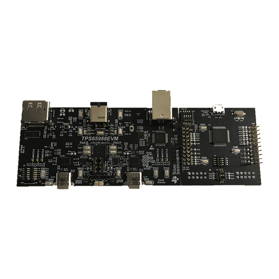
This document is the user guide for the TPS65988 Evaluation Module (TPS65988EVM). The
TPS65988EVM allows for evaluation of the TPS65988 IC as part of a stand-alone testing kit and for
development and testing of USB Type-C and Power Delivery (PD) end products. Out of the box, the
TPS65988EVM is configured to emulate a dual-port laptop computer. Both ports can be used to source or
sink power, and both are dual-role ports (DRP) but only support data as a downstream-facing port (DFP)
host. When different configurations are required to test your system, use the TPS65988 Application
Configuration software tool to create a configuration or load a different configuration template (see
Figure
1). The TPS65988EVM uses a control MUX (HD3SS3412) to route DisplayPort™ (DP) and a USB
HUB (TUSB8020) to route USB signals to the appropriate port A or port A (port A/B). The control MUX
and USB HUB are connected to a SuperSpeed (SS) MUX (TUSB546) which routes the appropriate DP
lanes and USB 3.0 signals according to cable orientation and Alternate Mode selection.
these features.
SLVUB62A – June 2017 – Revised June 2018
Submit Documentation Feedback
TPS65988 Evaluation Module
Figure 1. TPS65988EVM
Copyright © 2017–2018, Texas Instruments Incorporated
User's Guide
SLVUB62A – June 2017 – Revised June 2018
Figure 2
TPS65988 Evaluation Module
highlights
1
Advertisement
Table of Contents

Related Manuals for Texas Instruments TPS65988EVM


Summary of Contents for Texas Instruments TPS65988EVM
-
Page 1: Tps65988Evm
This document is the user guide for the TPS65988 Evaluation Module (TPS65988EVM). The TPS65988EVM allows for evaluation of the TPS65988 IC as part of a stand-alone testing kit and for development and testing of USB Type-C and Power Delivery (PD) end products. Out of the box, the TPS65988EVM is configured to emulate a dual-port laptop computer. -
Page 2: Tps65988Evm Block Diagram
MUX_CTR source L0-2 DP0-3 TUSB546 USB2 C_SSTX source USB3 Copyright © 2017, Texas Instruments Incorporated Figure 2. TPS65988EVM Block Diagram TPS65988 Evaluation Module SLVUB62A – June 2017 – Revised June 2018 Submit Documentation Feedback Copyright © 2017–2018, Texas Instruments Incorporated... -
Page 3: Table Of Contents
................TP13 (5 V), TP8 (3.3 V), and TP12 (1.2 V) ................. Aardvark™ Connector (J10) Schematic ....................Aardvark™ Connector (J10) SLVUB62A – June 2017 – Revised June 2018 TPS65988 Evaluation Module Submit Documentation Feedback Copyright © 2017–2018, Texas Instruments Incorporated... - Page 4 TPS65988EVM Processor Block ..................TPS65988EVM Power Path Block ..................TPS65988EVM Power Supply Block ..................TPS65988EVM DisplayPort Mux .................. TPS65988EVM SS MUX Block Port A .................. TPS65988EVM SS MUX Block Port B ....................TPS65988EVM USB HUB ................TPS65988EVM USB Type-C™ Port-A Block ................
- Page 5 DisplayPort™ and USB Test Setup ..................TPS65988EVM Bill of Materials Trademarks BoosterPack is a trademark of Texas Instruments. Dell is a registered trademark of Dell Incorporated. FTDI, Future Technology Devices International are registered trademarks of Future Technology Devices International Limited.
-
Page 6: About This Manual
This user guide describes how the TPS65988EVM can be used to test DisplayPort alternate mode as well as USB Data. This guide also contains testing procedures of DP alternate mode as well as various PD power configurations. -
Page 7: Setup
Related components are listed simultaneously. 5.1.1 Power Path Jumper Configuration The TPS65988EVM allows for analysis of TPS65987D and TPS65987S platforms through the adjustment of jumpers on J11 and J12. SLVUB62A – June 2017 – Revised June 2018 TPS65988 Evaluation Module Submit Documentation Feedback Copyright ©... -
Page 8: Tps65988 Jumper Configuration
5.1.1.1 TPS65988 Jumper Configuration Out of the box, the TPS65988EVM has jumper configuration for a TPS65988 device. With this configuration, the two internal power paths are configured as Source paths for their respective Type-C ports. The two external power paths are configured as Sink paths for their respective Type-C ports. When using the TPS65988EVM, use a TPS65988 template in the TPS6598x Application Customization Tool. -
Page 9: Tps65987D Jumper Configuration
TPS65987D Jumper Configuration To use the TPS65988EVM to perform as a TPS65987D, the jumpers on J11 and J12 needs to be adjusted. Place a jumper on J12 to short the two VBUS nodes together. In this use case, one of the internal power paths is used as a source path and the other internal power path is used as a sink path. -
Page 10: Tps65987S Jumper Configuration
5.1.1.3 TPS65987S Jumper Configuration To emulate a TPS65987S with the TPS65988EVM, the jumpers on J11 need to be adjusted. The TPS65987S supports one Type-C port and contains one internal power path. When using the TPS65988EVM to emulate a TPS65987S, the internal power path (PPHV1) is used as the Source Path and one of the external power paths is used as the sink path. -
Page 11: Displayport™ Source Schematic Block
Port B BDP0 BDP1 TUSB546 BDP2 BDP3 Copyright © 2017, Texas Instruments Incorporated Figure 10. DisplayPort™ Source Block Diagram Figure 11. DisplayPort™ Source Receptacle SLVUB62A – June 2017 – Revised June 2018 TPS65988 Evaluation Module Submit Documentation Feedback Copyright © 2017–2018, Texas Instruments Incorporated... -
Page 12: Hreset Push-Button (S1) Schematic
HRESET ADCIN1 ADCIN2 HRESET P3V3 0.01µF 100k Figure 12. HRESET Push-Button (S1) Schematic Figure 13. HRESET Push-Button (S1) TPS65988 Evaluation Module SLVUB62A – June 2017 – Revised June 2018 Submit Documentation Feedback Copyright © 2017–2018, Texas Instruments Incorporated... -
Page 13: Spi-Miso Pull Down Switch
F_SPI_CLK R212 F_I2C_IRQ1 R215 I2C1_SCL R218 R219 F_SWD_DATA I2C1_SDA R222 R223 F_SWD_CLK Figure 15. FTDI Dip Switch (S3) Schematic ® SLVUB62A – June 2017 – Revised June 2018 TPS65988 Evaluation Module Submit Documentation Feedback Copyright © 2017–2018, Texas Instruments Incorporated... -
Page 14: Ftdi ® Dip Switch (S3)
S2: SPI , I C, and BusPowerZ Configurations The TPS65988EVM has a dip switch (S2) that can be used to configure the I C addresses and BusPower settings of the device. Switch1 through Switch3 are used to set the I2C address of the TPS65988 by adjusting the voltage divider seen at ADCIN2. -
Page 15: C And Buspower Dip Switch (S2)
Setup www.ti.com Figure 17. I C and BusPower DIP Switch (S2) Figure 18. I C DIP Switch (S2) Schematic SLVUB62A – June 2017 – Revised June 2018 TPS65988 Evaluation Module Submit Documentation Feedback Copyright © 2017–2018, Texas Instruments Incorporated... -
Page 16: Barrel Jack (J1) Schematic
SHIELD POWER SHIELD SHIELD SENSE POWER JPD1135-509-7F 100k 11.0k Figure 19. Barrel Jack (J1) Schematic Figure 20. Barrel Jack (J1) TPS65988 Evaluation Module SLVUB62A – June 2017 – Revised June 2018 Submit Documentation Feedback Copyright © 2017–2018, Texas Instruments Incorporated... -
Page 17: Barrel Jack Detect Schematic
5.1.8 Barrel Jack Detect The TPS65988EVM is capable of requesting a power role swap when the barrel jack is connected on an EVM that is currently bus-powered. The barrel jack voltage is sensed by a comparator, which drives GPIO1 (BJ_DETECT) on the TPS65988. By default, the Barrel Jack Detect is not enabled. To enable Barrel Jack Detect place R109 and refer to the TPS65988 Utilities Tool User Guide and TPS65988 Firmware User Guide. -
Page 18: Usb Type-B Receptacle (J11)
Setup www.ti.com Figure 24. USB Type-B Receptacle (J11) TPS65988 Evaluation Module SLVUB62A – June 2017 – Revised June 2018 Submit Documentation Feedback Copyright © 2017–2018, Texas Instruments Incorporated... -
Page 19: Usb Type-C™ Receptacles (J2) Schematic
5.1.10 USB Type-C™Connector (J2) The TPS65988EVM has two full feature USB Type-C receptacles (port A/B) and routes VBUS, SSTX and SSRX pairs, SBU1 and SBU2 pairs, and D+ and D– signals. The TPS65988 device can be used in self- powered and bus-powered configurations for added flexibility. When self-powered, the EVM can provide up to 60 W (20 V, at 3 A) of power per port via the internal high voltage power path. -
Page 20: Usb Micro-B Receptacle (J9) Schematic
F_USB_D_N 26 ohm F_5V_VBUS VBUS C143 0.01µF Figure 27. USB Micro-B Receptacle (J9) Schematic Figure 28. USB Micro-B Receptacle (J9) TPS65988 Evaluation Module SLVUB62A – June 2017 – Revised June 2018 Submit Documentation Feedback Copyright © 2017–2018, Texas Instruments Incorporated... -
Page 21: Tp13 (5 V), Tp8 (3.3 V), And Tp12 (1.2 V)
These test points allow the user to verify the system supplies on the TPS65988EVM. LDO_1V8 is internally generated for internal circuitry. Use P3V3 to supply VIN_3V3 which then supplies LDO_3V3. Also, use LDO_3V3 as a low- power output for external flash memory. -
Page 22: Aardvark™ Connector (J10) Schematic
GND planes through multiple vias.Figure 32 highlights these features. Figure 32. TP10, TP11, TP15, TP16, TP17, TP18, TP9: GND Test Points TPS65988 Evaluation Module SLVUB62A – June 2017 – Revised June 2018 Submit Documentation Feedback Copyright © 2017–2018, Texas Instruments Incorporated... -
Page 23: Tp1, Tp2, Tp3 And Tp4 - Cc1 And Cc2 Test Points
Figure 33. TP1, TP2, TP3 and TP4 – CC1 and CC2 Test Points Figure 34. TPS65988 BMC Data SLVUB62A – June 2017 – Revised June 2018 TPS65988 Evaluation Module Submit Documentation Feedback Copyright © 2017–2018, Texas Instruments Incorporated... -
Page 24: Vbus Test Points: Tp14
20 V, use caution when connecting and disconnecting probes on the TPS65988EVM. The VBUS test point is capable of drawing up to 3 A for an external load. Note that a PD power contract with the necessary capability must be negotiated in order to draw current from the VBUS test point. -
Page 25: Var, B-Var And System Power Test Points: Tp7, Tp6, And Tp5
20 V decreases the sourcing power capabilities. Figure 37 highlights these features. Figure 37. A-Var, B-Var and System Power Test Points: TP7, TP6, and TP5 SLVUB62A – June 2017 – Revised June 2018 TPS65988 Evaluation Module Submit Documentation Feedback Copyright © 2017–2018, Texas Instruments Incorporated... -
Page 26: Led Indicators Description
5.1.18 J3 and J4 (Bottom of EVM): Signal Headers These headers allow the user to probe many different signals on the TPS65988EVM. Note that some of the header pins are not connected unless a 0-Ω option resistor is placed. Figure 38 highlights these features. -
Page 27: Mux Control Leds
USB 3.0 event D18 - MXCTL1 GPIO5 DP mode event D19 - MXCTL2 GPIO7 Cable orientation event D24 - PA_HPD GPIO3 SLVUB62A – June 2017 – Revised June 2018 TPS65988 Evaluation Module Submit Documentation Feedback Copyright © 2017–2018, Texas Instruments Incorporated... -
Page 28: Pdo Port A/B Leds
D22 - PB_PDO0 GPIO_15 PDO TT bit 0 D5 - PA_VAR_DCDC GPIO_16 VAR-A enable D3 - PB_VAR_DCDC GPIO_17 VAR-B enable TPS65988 Evaluation Module SLVUB62A – June 2017 – Revised June 2018 Submit Documentation Feedback Copyright © 2017–2018, Texas Instruments Incorporated... -
Page 29: Pdo Led 0 And Pdo Led 1 Truth Table
011b 0.90 Table 6. ADCIN1 Setting Switch On, Off Bits Divider Ratio 000b 0.00 001b 0.34 010b 0.50 011b 0.90 SLVUB62A – June 2017 – Revised June 2018 TPS65988 Evaluation Module Submit Documentation Feedback Copyright © 2017–2018, Texas Instruments Incorporated... -
Page 30: Using The Tps65988Evm
Firmware Configurations Out of the box, the TPS65988EVM is configured to emulate a dual-port laptop computer. Both ports are used to source or sink power, and both ports are data DFP. If different configurations are required to test your system, use the TPS65988 Application Configuration GUI tool to create a configuration or load a different configuration template. -
Page 31: Connecting Evm To Usb Type-C™ Device
7.1.2 Connecting to USB Type-C™ Devices Using a USB Type-C cable allows for connection to USB and DP devices. When a TPS65988EVM is used with a TPS6598x-EVM as DP source and sink boards respectively, a complete USB Type-C system can be verified. - Page 32 Dell laptop power supply (model # 492-BBGP) Use the TPS65988EVM to test DP alternate mode as well as USB data using the default firmware. To do so, connect a DP source from a laptop to the TPS65988EVM through the DP receptacle on the EVM.
-
Page 33: Displayport™ And Usb Test Setup
DP can optionally be connected from port A/B with a USB Type-C to DP cable. SLVUB62A – June 2017 – Revised June 2018 TPS65988 Evaluation Module Submit Documentation Feedback Copyright © 2017–2018, Texas Instruments Incorporated... - Page 34 ‘sink preferred’ dip switch configuration (for ex. configuration ID1: 1000) (refer to TPS6598x EVM user guide for more info) TPS65988 Evaluation Module SLVUB62A – June 2017 – Revised June 2018 Submit Documentation Feedback Copyright © 2017–2018, Texas Instruments Incorporated...
- Page 35 Table 7. DisplayPort™ and USB Test Setup (continued) Test Setup Pass Criteria USB can optionally be connected to Port A/B directly with a Type-C Flash Drive SLVUB62A – June 2017 – Revised June 2018 TPS65988 Evaluation Module Submit Documentation Feedback Copyright © 2017–2018, Texas Instruments Incorporated...
- Page 36 Connect a type C cable from DP and USB can optionally be tested with the TPS65988EVM setup to the right. TPS65988 Evaluation Module SLVUB62A – June 2017 – Revised June 2018 Submit Documentation Feedback Copyright © 2017–2018, Texas Instruments Incorporated...
-
Page 37: Dp And Usb Test Setup
USB 3.0 data can be confirmed by observing LED MUX_CTRL0 in the high state. Figure 45 highlights this test setup. Figure 45. DP and USB Test Setup SLVUB62A – June 2017 – Revised June 2018 TPS65988 Evaluation Module Submit Documentation Feedback Copyright © 2017–2018, Texas Instruments Incorporated... -
Page 38: Debugging The Evm
Verify that VBUS is reaching 5 V when connected, (see Figure Figure 46. DRP CC1 and CC2 Toggling Figure 47. USB Type-C™ Connection and VBUS TPS65988 Evaluation Module SLVUB62A – June 2017 – Revised June 2018 Submit Documentation Feedback Copyright © 2017–2018, Texas Instruments Incorporated... -
Page 39: Usb Type-C™ Connection And Pd Negotiation
Check for a small spike on VBUS during a plug event to verify that the PP_HV or PP_EXT switch is closed and is then opened, once an overcurrent condition is detected. Figure 48. USB Type-C™ Connection and PD Negotiation SLVUB62A – June 2017 – Revised June 2018 TPS65988 Evaluation Module Submit Documentation Feedback Copyright © 2017–2018, Texas Instruments Incorporated... -
Page 40: Tps65988Evm Schematic
TPS65988EVM Schematic Figure 49 shows the block diagram of the main components of the TPS65988EVM. The main schematic blocks port A/B control MUX and SS MUX, USB HUB, power paths, power supplies, USB Type-C receptacles, processor, BoosterPack headers, and hardware. -
Page 41: Tps65988Evm Processor Block
USB Type-C PD controller and contains connections for GPIOs, D+ and D-, CC1 and CC2, HRESET, I C lines, SPI for flash memory, and ADC1 and ADC2. Figure 50. TPS65988EVM Processor Block SLVUB62A – June 2017 – Revised June 2018 TPS65988 Evaluation Module Submit Documentation Feedback Copyright ©... -
Page 42: Tps65988Evm Power Path Block
PMOS with RCP circuit. The internal power path is used for sourcing power and the external power path is used for sinking power. The TPS65988 power path can provide power to VBUS or consume power from VBUS. Figure 51. TPS65988EVM Power Path Block TPS65988 Evaluation Module SLVUB62A –... -
Page 43: Tps65988Evm Power Supply Block
SYS_PWR is 5 V; however, this also decreases VBUS maximum power capabilities. When using a lower voltage, the comparator circuit may have to be adjusted to trip at a lower voltage for proper barrel jack detection. Figure 52. TPS65988EVM Power Supply Block SLVUB62A – June 2017 – Revised June 2018... -
Page 44: Tps65988Evm Displayport Mux
TPS65988EVM Schematic www.ti.com Figure 53 shows the DisplayPort Mux used to switch the DisplayPort signals to either Type-C Port. Figure 53. TPS65988EVM DisplayPort Mux TPS65988 Evaluation Module SLVUB62A – June 2017 – Revised June 2018 Submit Documentation Feedback Copyright © 2017–2018, Texas Instruments Incorporated... -
Page 45: Tps65988Evm Ss Mux Block Port A
SS MUX is capable of USB 3.1 data rates up to 5 Gbps and DP 1.4 up to 8.1 Gbps with 2 or 4 DP lanes. Figure 54. TPS65988EVM SS MUX Block Port A SLVUB62A – June 2017 – Revised June 2018... -
Page 46: Tps65988Evm Ss Mux Block Port B
C. As the host, the SS MUX is capable of USB 3.1 data rates up to 5 Gbps and DP 1.4 up to 8.1 Gbps with 2 or 4 DP lanes. Figure 55. TPS65988EVM SS MUX Block Port B TPS65988 Evaluation Module SLVUB62A –... -
Page 47: Tps65988Evm Usb Hub
TPS65988EVM Schematic www.ti.com Figure 56 shows the U.SB HUB, which contains the connections from the USB source receptacle. Figure 56. TPS65988EVM USB HUB SLVUB62A – June 2017 – Revised June 2018 TPS65988 Evaluation Module Submit Documentation Feedback Copyright © 2017–2018, Texas Instruments Incorporated... -
Page 48: Tps65988Evm Usb Type-C™ Port-A Block
TPS65988EVM Schematic www.ti.com Figure 57 shows the USB Type-C block, which includes the USB Type-C port A and ESD protection. Figure 57. TPS65988EVM USB Type-C™ Port-A Block TPS65988 Evaluation Module SLVUB62A – June 2017 – Revised June 2018 Submit Documentation Feedback... -
Page 49: Tps65988Evm Usb Type-C™ Port B Block
Figure 58 shows the USB Type-C block, which includes the USB Type-C port B and ESD protection. Figure 58. TPS65988EVM USB Type-C™ Port B Block SLVUB62A – June 2017 – Revised June 2018 TPS65988 Evaluation Module Submit Documentation Feedback... -
Page 50: Tps65988Evm Ftdi Connector Block
Figure 59 shows the FTDI block, which contain the connections from the FTDI board. Figure 59. TPS65988EVM FTDI Connector Block ® TPS65988 Evaluation Module SLVUB62A – June 2017 – Revised June 2018 Submit Documentation Feedback Copyright © 2017–2018, Texas Instruments Incorporated... -
Page 51: Tps65988Evm Current Sense Block Port A
Figure 61 show the current sense block, which contain the sense connections to VBUS and VIN_3V3 for port A and port B. Figure 60. TPS65988EVM Current Sense Block Port A Figure 61. TPS65988EVM Current Sense Block Port B SLVUB62A – June 2017 – Revised June 2018... -
Page 52: Tps65988Evm Boosterpack Header Block
TPS65988EVM Schematic www.ti.com Figure 62 shows the BoosterPack headers block, which contain the connections to the BoosterPack headers. Figure 62. TPS65988EVM BoosterPack Header Block TPS65988 Evaluation Module SLVUB62A – June 2017 – Revised June 2018 Submit Documentation Feedback Copyright © 2017–2018, Texas Instruments Incorporated... -
Page 53: Tps65988Evm Board Layout
TPS65988EVM Board Layout Figure 49 through Figure 74 contain the PCB layouts of the TPS65988EVM. Figure 63. TPS65988EVM Top Overlay Figure 64. TPS65988EVM Top Layer Component View Figure 65. TPS65988EVM SSTXRX1 SLVUB62A – June 2017 – Revised June 2018... -
Page 54: Tps65988Evm Gnd Plane 1
TPS65988EVM Board Layout www.ti.com Figure 66. TPS65988EVM GND Plane 1 Figure 67. TPS65988EVM High Speed Figure 68. TPS65988EVM GND Plane 2 TPS65988 Evaluation Module SLVUB62A – June 2017 – Revised June 2018 Submit Documentation Feedback Copyright © 2017–2018, Texas Instruments Incorporated... -
Page 55: Tps65988Evm Power 1
TPS65988EVM Board Layout www.ti.com Figure 69. TPS65988EVM Power 1 Figure 70. TPS65988EVM Power 2 Figure 71. TPS65988EVM GND Plane 3 SLVUB62A – June 2017 – Revised June 2018 TPS65988 Evaluation Module Submit Documentation Feedback Copyright © 2017–2018, Texas Instruments Incorporated... -
Page 56: Tps65988Evm Sstxrx2
TPS65988EVM Board Layout www.ti.com Figure 72. TPS65988EVM SSTXRX2 Figure 73. TPS65988EVM Bottom Overlay Figure 74. TPS65988EVM Bottom Layer Component View TPS65988 Evaluation Module SLVUB62A – June 2017 – Revised June 2018 Submit Documentation Feedback Copyright © 2017–2018, Texas Instruments Incorporated... -
Page 57: Tps65988Evm Bill Of Materials
TPS65988EVM Bill of Materials www.ti.com TPS65988EVM Bill of Materials Table 8 lists the TPS65988EVM BOM. Table 8. TPS65988EVM Bill of Materials Designator Value Description Package Reference Part Number Manufacturer Alternate Part Alternate Number Manufacturer !PCB1 Printed Circuit Board ACS009 C1, C24_PA_SS, 0.1uF... - Page 58 TPS65988EVM Bill of Materials www.ti.com Table 8. TPS65988EVM Bill of Materials (continued) Designator Value Description Package Reference Part Number Manufacturer Alternate Part Alternate Number Manufacturer C15, C16 22uF CAP, CERM, 22 µF, 10 V, +/- 20%, X5R, 0603 0603 C1608X5R1A226M080AC...
- Page 59 TPS65988EVM Bill of Materials www.ti.com Table 8. TPS65988EVM Bill of Materials (continued) Designator Value Description Package Reference Part Number Manufacturer Alternate Part Alternate Number Manufacturer Diode, TVS, Bi, 24 V, 200 W, SOD323, 2-Leads, Body SOD323, 2-Leads, Body PESD24VL1BA,115 NXP Semiconductor 1.9x1.45mm, No Polarity Mark...
- Page 60 TPS65988EVM Bill of Materials www.ti.com Table 8. TPS65988EVM Bill of Materials (continued) Designator Value Description Package Reference Part Number Manufacturer Alternate Part Alternate Number Manufacturer Q3, Q6, Q11, Q17, MOSFET, N-CH, 20 V, 0.5 A, YJM0003A (PICOSTAR-3) YJM0003A CSD15380F3 Texas Instruments...
- Page 61 TPS65988EVM Bill of Materials www.ti.com Table 8. TPS65988EVM Bill of Materials (continued) Designator Value Description Package Reference Part Number Manufacturer Alternate Part Alternate Number Manufacturer R28, R39, R53_PA_SS, 1.00k RES, 1.00 k, 1%, 0.05 W, 0201 0201 CRCW02011K00FKED Vishay-Dale R53_PB_SS,...
- Page 62 TPS65988EVM Bill of Materials www.ti.com Table 8. TPS65988EVM Bill of Materials (continued) Designator Value Description Package Reference Part Number Manufacturer Alternate Part Alternate Number Manufacturer R195 1.00k RES, 1.00 k, 1%, 0.1 W, 0603 0603 CRCW06031K00FKEA Vishay-Dale R208, R211, R212, RES, 0, 5%, 0.1 W, 0603...
- Page 63 TPS65988EVM Bill of Materials www.ti.com Table 8. TPS65988EVM Bill of Materials (continued) Designator Value Description Package Reference Part Number Manufacturer Alternate Part Alternate Number Manufacturer Nanopower, 1.8V, Comparator with Voltage Reference, DCK0006A TLV3012AIDCKR Texas Instruments TLV3012AIDCKT Texas Instruments DCK0006A U12_PA, U12_PB...
- Page 64 TPS65988EVM Bill of Materials www.ti.com Table 8. TPS65988EVM Bill of Materials (continued) Designator Value Description Package Reference Part Number Manufacturer Alternate Part Alternate Number Manufacturer R58_PB_SS, 1.00k RES, 1.00 k, 1%, 0.05 W, 0201 0201 CRCW02011K00FKED Vishay-Dale R59_PA_SS, R59_PB_SS, R60_PA_SS,...
- Page 65 Changes from Original (June 2017) to A Revision ......................Page ........... • Overall rework of this user's guide for revision A from Section 4 Section SLVUB62A – June 2017 – Revised June 2018 Revision History Submit Documentation Feedback Copyright © 2017–2018, Texas Instruments Incorporated...
- Page 66 STANDARD TERMS FOR EVALUATION MODULES Delivery: TI delivers TI evaluation boards, kits, or modules, including any accompanying demonstration software, components, and/or documentation which may be provided together or separately (collectively, an “EVM” or “EVMs”) to the User (“User”) in accordance with the terms set forth herein.
- Page 67 FCC Interference Statement for Class B EVM devices NOTE: This equipment has been tested and found to comply with the limits for a Class B digital device, pursuant to part 15 of the FCC Rules. These limits are designed to provide reasonable protection against harmful interference in a residential installation.
- Page 68 【無線電波を送信する製品の開発キットをお使いになる際の注意事項】 開発キットの中には技術基準適合証明を受けて いないものがあります。 技術適合証明を受けていないもののご使用に際しては、電波法遵守のため、以下のいずれかの 措置を取っていただく必要がありますのでご注意ください。 1. 電波法施行規則第6条第1項第1号に基づく平成18年3月28日総務省告示第173号で定められた電波暗室等の試験設備でご使用 いただく。 2. 実験局の免許を取得後ご使用いただく。 3. 技術基準適合証明を取得後ご使用いただく。 なお、本製品は、上記の「ご使用にあたっての注意」を譲渡先、移転先に通知しない限り、譲渡、移転できないものとします。 上記を遵守頂けない場合は、電波法の罰則が適用される可能性があることをご留意ください。 日本テキサス・イ ンスツルメンツ株式会社 東京都新宿区西新宿6丁目24番1号 西新宿三井ビル 3.3.3 Notice for EVMs for Power Line Communication: Please see http://www.tij.co.jp/lsds/ti_ja/general/eStore/notice_02.page 電力線搬送波通信についての開発キットをお使いになる際の注意事項については、次のところをご覧ください。http:/ /www.tij.co.jp/lsds/ti_ja/general/eStore/notice_02.page 3.4 European Union 3.4.1 For EVMs subject to EU Directive 2014/30/EU (Electromagnetic Compatibility Directive): This is a class A product intended for use in environments other than domestic environments that are connected to a low-voltage power-supply network that supplies buildings used for domestic purposes.
- Page 69 Notwithstanding the foregoing, any judgment may be enforced in any United States or foreign court, and TI may seek injunctive relief in any United States or foreign court. Mailing Address: Texas Instruments, Post Office Box 655303, Dallas, Texas 75265 Copyright © 2018, Texas Instruments Incorporated...
- Page 70 IMPORTANT NOTICE FOR TI DESIGN INFORMATION AND RESOURCES Texas Instruments Incorporated (‘TI”) technical, application or other design advice, services or information, including, but not limited to, reference designs and materials relating to evaluation modules, (collectively, “TI Resources”) are intended to assist designers who are developing applications that incorporate TI products;...
Need help?
Do you have a question about the TPS65988EVM and is the answer not in the manual?
Questions and answers