Ublox TOBY-L2 Series System Integration Manual
Lte/dc-hspa+/egprs modules
Hide thumbs
Also See for TOBY-L2 Series:
- System integration manual (141 pages) ,
- User manual (31 pages) ,
- System integration manual (158 pages)
Table of Contents
Advertisement
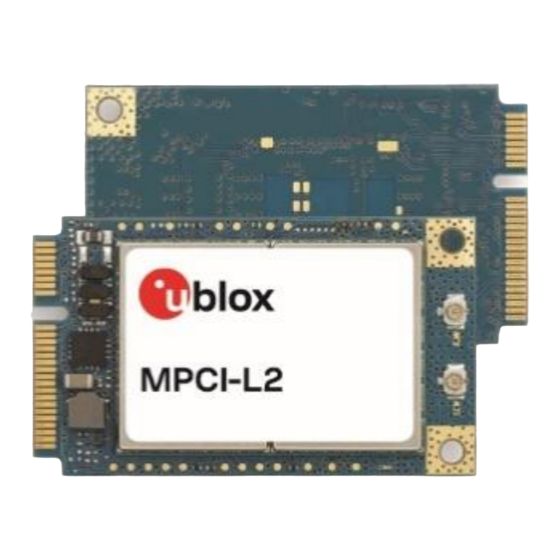
TOBY-L2 and MPCI-L2 series
LTE/DC-HSPA+/EGPRS modules
System Integration Manual
Abstract
This document describes the features and the system integration of TOBY-L2 and MPCI-L2 series
multi-mode cellular modules. These modules are a complete and cost efficient LTE/3G/2G solution
offering up to 150 Mb/s download and 50 Mb/s upload data rates, covering up to six LTE bands, up
to five WCDMA/DC-HSPA+ bands and up to four GSM/EGPRS bands in the compact TOBY LGA form
factor of TOBY-L2 modules or in the industry standard PCI Express Mini Card form factor of MPCI-L2
modules.
www.u-blox.com
UBX-13004618 - R28
Advertisement
Table of Contents

Related Manuals for Ublox TOBY-L2 Series


Summary of Contents for Ublox TOBY-L2 Series
- Page 1 TOBY-L2 and MPCI-L2 series LTE/DC-HSPA+/EGPRS modules System Integration Manual Abstract This document describes the features and the system integration of TOBY-L2 and MPCI-L2 series multi-mode cellular modules. These modules are a complete and cost efficient LTE/3G/2G solution offering up to 150 Mb/s download and 50 Mb/s upload data rates, covering up to six LTE bands, up to five WCDMA/DC-HSPA+ bands and up to four GSM/EGPRS bands in the compact TOBY LGA form factor of TOBY-L2 modules or in the industry standard PCI Express Mini Card form factor of MPCI-L2 modules.
-
Page 2: Document Information
TOBY-L2 and MPCI-L2 series - System Integration Manual Document Information Title TOBY-L2 and MPCI-L2 series Subtitle LTE/DC-HSPA+/EGPRS modules Document type System Integration Manual Document number UBX-13004618 Revision and date 12-Apr-2019 Disclosure Restriction Product status Corresponding content status Functional Sample Draft For functional testing. -
Page 3: Table Of Contents
TOBY-L2 and MPCI-L2 series - System Integration Manual This document applies to the following products: Product status Product name Type number Modem version Application version PCN reference TOBY-L200 TOBY-L200-00S-00 09.71 A01.15 UBX-14044437 Obsolete TOBY-L200-00S-01 09.71 A01.30 UBX-16026448 Obsolete TOBY-L200-02S-00 15.90 A01.00 UBX-15029946 Obsolete... -
Page 4: Contents
Overview ................................ 8 1.2 Architecture ..............................11 1.2.1 Internal blocks ............................ 12 1.3 Pin-out ................................. 13 1.3.1 TOBY-L2 series pin assignment ....................13 1.3.2 MPCI-L2 series pin assignment ...................... 17 1.4 Operating modes ............................19 1.5 Supply interfaces ............................21 1.5.1 Module supply input (VCC or 3.3Vaux) .................. - Page 5 2.9 Mini PCIe specific signals (W_DISABLE#, LED_WWAN#) ............... 117 2.10 Reserved pins (RSVD) ..........................118 2.11 Module placement ........................... 119 2.12 TOBY-L2 series module footprint and paste mask ................. 120 2.13 MPCI-L2 series module installation ..................... 121 2.14 Thermal guidelines ..........................122 2.15 ESD guidelines ............................
- Page 6 TOBY-L2 and MPCI-L2 series - System Integration Manual 2.15.2 ESD immunity test of TOBY-L2 and MPCI-L2 reference design .......... 125 2.15.3 ESD application circuits ........................ 125 2.16 Schematic for TOBY-L2 and MPCI-L2 module integration ............128 2.16.1 Schematic for TOBY-L2 module “00” product version ............128 2.16.2 Schematic for TOBY-L2 module “01”...
- Page 7 TOBY-L2 and MPCI-L2 series - System Integration Manual 5.1 u-blox in-series production test ......................149 5.2 Test parameters for OEM manufacturer ................... 150 5.2.1 “Go/No go” tests for integrated devices ..................150 5.2.2 RF functional tests ......................... 150 Appendix ..............................152 Migration between TOBY-L1 and TOBY-L2 ................
-
Page 8: System Description
TOBY-L2 and MPCI-L2 series - System Integration Manual System description Overview TOBY-L2 and MPCI-L2 series comprises LTE/3G/2G multi-mode modules supporting up to six LTE bands, up to five UMTS/DC-HSPA+ bands and up to four GSM/(E)GPRS bands for voice and/or data transmission as following: ... -
Page 9: Ubx-13004618 - R28
TOBY-L2 and MPCI-L2 series - System Integration Manual Table 1 summarizes the TOBY-L2 and MPCI-L2 series main features and interfaces. Module UMTS Interfaces Audio Features Grade 2,4,5 1,2,4 TOBY-L200 Quad ♦ ● ♦ ♦ ♦ ♦ ● ♦ ● ♦ ♦... -
Page 10: Ubx-13004618 - R28
TOBY-L2 and MPCI-L2 series - System Integration Manual 4G LTE 3G UMTS/HSDPA/HSUPA 2G GSM/GPRS/EDGE 3GPP Release 9 3GPP Release 8 3GPP Release 8 Long Term Evolution (LTE) Dual-Cell HS Packet Access (DC-HSPA+) Enhanced Data rate GSM Evolution (EDGE) Evolved UTRA (E-UTRA) UMTS Terrestrial Radio Access (UTRA) GSM EGPRS Radio Access (GERA) Frequency Division Duplex (FDD) -
Page 11: Architecture
External Reset V_INT (I/O) Figure 1: TOBY-L2 series block diagram As described in the Figure 2, each MPCI-L2 series module integrates one TOBY-L2 series module: The MPCI-L200 integrates a TOBY-L200 module The MPCI-L201 integrates a TOBY-L201 module ... -
Page 12: Internal Blocks
Internal blocks As described in Figure 2, each MPCI-L2 series module integrates one TOBY-L2 series module, which consists of the following internal sections: RF, baseband and power management. RF section The RF section is composed of RF transceiver, PAs, LNAs, crystal oscillator, filters, duplexers and RF switches. -
Page 13: Pin-Out
TOBY-L2 and MPCI-L2 series - System Integration Manual 1.3 Pin-out 1.3.1 TOBY-L2 series pin assignment Table 3 lists the pin-out of the TOBY-L2 series modules, with pins grouped by function. Function Pin name Pin No Description Remarks Power 70,71,72 Module supply input VCC pins are internally connected each other. -
Page 14: Ubx-13004618 - R28
TOBY-L2 and MPCI-L2 series - System Integration Manual Function Pin name Pin No Description Remarks VSIM SIM supply output VSIM = 1.8 V / 3 V output as per connected SIM type. See section for functional description. See section for external circuit design-in. SIM_IO SIM data Data input/output for 1.8 V / 3 V SIM... -
Page 15: Ubx-13004618 - R28
TOBY-L2 and MPCI-L2 series - System Integration Manual Function Pin name Pin No Description Remarks UART UART data output Not supported by “00” product versions. 1.8 V output, Circuit 104 (RXD) in ITU-T V.24, for AT and data communication, FOAT, diagnostic. Test-Point and series 0 ... -
Page 16: Ubx-13004618 - R28
TOBY-L2 and MPCI-L2 series - System Integration Manual Function Pin name Pin No Description Remarks C bus clock line Not supported by versions ‘00’, ‘01’, ‘60’, TOBY-L201-02S. 1.8 V open drain, to communicate with I2C-slave devices. External pull-up required. See section 1.9.3 for functional description. -
Page 17: Mpci-L2 Series Pin Assignment
See section 2.10 33-43, 45, 47-49, 77, 84, 91 Table 3: TOBY-L2 series module pin definition, grouped by function 1.3.2 MPCI-L2 series pin assignment Table 4 lists the pin-out of the MPCI-L2 series modules, with pins grouped by function. Function... -
Page 18: Ubx-13004618 - R28
TOBY-L2 and MPCI-L2 series - System Integration Manual Function Pin name Pin No Description Remarks Antennas ANT1 U.FL Primary antenna Main Tx / Rx antenna interface. 50 nominal characteristic impedance. Antenna circuit affects RF performance and integrating device compliance with applicable certification schemes. See section for functional description / requirements. -
Page 19: Operating Modes
TOBY-L2 and MPCI-L2 series - System Integration Manual Operating modes TOBY-L2 and MPCI-L2 series modules have several operating modes. The operating modes are defined in Table 5 and described in detail in Table 6, providing general guidelines for operation. General Status Operating Mode Definition Power-down... -
Page 20: Ubx-13004618 - R28
TOBY-L2 and MPCI-L2 series - System Integration Manual Operating Mode Description Transition between operating modes Active-Mode Module is switched on with application When the module is switched on by an appropriate interfaces enabled or not suspended: the power-on event (see 1.6.1), the module enters active-mode module is ready to communicate with an from power-off mode. -
Page 21: Supply Interfaces
TOBY-L2 and MPCI-L2 series - System Integration Manual 1.5 Supply interfaces 1.5.1 Module supply input (VCC or 3.3Vaux) TOBY-L2 modules are supplied via the three VCC pins, and MPCI-L2 modules are supplied via the five 3.3Vaux pins. All supply voltages used inside the modules are generated from the VCC or the 3.3Vaux supply input by integrated voltage regulators, including the V_BCKP RTC supply, the V_INT generic digital interface supply, and the VSIM or UIM_PWR SIM interface supply. -
Page 22: Ubx-13004618 - R28
TOBY-L2 and MPCI-L2 series - System Integration Manual 1.5.1.2 Current consumption in 2G connected-mode When a GSM call is established, the VCC or 3.3Vaux module current consumption is determined by the current consumption profile typical of the GSM transmitting and receiving bursts. The peak of current consumption during a transmission slot is strictly dependent on the RF transmitted power, which is regulated by the network (the current base station). -
Page 23: Ubx-13004618 - R28
TOBY-L2 and MPCI-L2 series - System Integration Manual When a GPRS connection is established, more than one slot can be used to transmit and/or more than one slot can be used to receive. The transmitted power depends on network conditions, which set the peak current consumption, but following the 3GPP specifications the maximum Tx RF power is reduced if more than one slot is used to transmit, so the maximum peak of current is not as high as can be in case of a 2G single-slot call. -
Page 24: Ubx-13004618 - R28
TOBY-L2 and MPCI-L2 series - System Integration Manual 1.5.1.3 Current consumption in 3G connected mode During a 3G connection, the module can transmit and receive continuously due to the Frequency Division Duplex (FDD) mode of operation with the Wideband Code Division Multiple Access (WCDMA). The current consumption depends on output RF power, which is always regulated by the network (the current base station) sending power control commands to the module. -
Page 25: Ubx-13004618 - R28
TOBY-L2 and MPCI-L2 series - System Integration Manual 1.5.1.4 Current consumption in LTE connected-mode During an LTE connection, the module can transmit and receive continuously due to the Frequency Division Duplex (FDD) mode of operation used in LTE radio access technology. The current consumption depends on output RF power, which is always regulated by the network (the current base station) sending power control commands to the module. -
Page 26: Ubx-13004618 - R28
TOBY-L2 and MPCI-L2 series - System Integration Manual 1.5.1.5 Current consumption in cyclic idle/active mode (power saving enabled) The power saving configuration is by default disabled, but it can be enabled using the AT+UPSV command (see the u-blox AT Commands Manual [3]). When power saving is enabled, the module automatically enters the low power idle-mode whenever possible, reducing current consumption. -
Page 27: Ubx-13004618 - R28
TOBY-L2 and MPCI-L2 series - System Integration Manual 1.5.1.6 Current consumption in fixed active-mode (power saving disabled) When power saving is disabled, the module does not automatically enter the low power idle-mode whenever possible: the module remains in active-mode. Power saving configuration is by default disabled. -
Page 28: Rtc Supply Input/Output (V_Bckp)
The RTC supply V_BCKP pin is not available on MPCI-L2 series modules. The V_BCKP pin of TOBY-L2 series modules connects the supply for the Real Time Clock (RTC). A linear LDO regulator integrated in the Power Management Unit internally generates this supply, as... -
Page 29: Generic Digital Interfaces Supply Output (V_Int)
The generic digital interfaces supply V_INT pin is not available on MPCI-L2 series modules. The V_INT output pin of the TOBY-L2 series modules is connected to an internal 1.8 V supply with current capability specified in the TOBY-L2 series Data Sheet [1]. This supply is internally generated... -
Page 30: System Function Interfaces
13, the TOBY-L2 series PWR_ON input is equipped with an internal active pull-up resistor to the VCC module supply: the PWR_ON input voltage thresholds are different from the other generic digital interfaces. Detailed electrical characteristics are described in TOBY-L2 series Data Sheet [1]. -
Page 31: Ubx-13004618 - R28
TOBY-L2 and MPCI-L2 series - System Integration Manual Figure 14 shows the module power-on sequence from the not-powered mode, with following phases: The external supply is applied to VCC or 3.3Vaux supply inputs, representing the start-up event. PWR_ON and RESET_N or PERST# pins suddenly rise to high logic level due to internal pull-ups. ... -
Page 32: Module Power-Off
3.3Vaux supply can be removed. An abrupt hardware shutdown occurs on TOBY-L2 series modules when a low level is applied on the RESET_N pin for a specific time period. In this case, the current parameter settings are not saved in the module’s non-volatile memory and a proper network detach is not performed. -
Page 33: Ubx-13004618 - R28
Tristate / Floating BB Pads State Operational Figure 15: TOBY-L2 series power-off sequence description ☞ The Internal Reset signal is not available on a module pin, but it is recommended monitoring the V_INT pin to sense the end of the internal switch-off sequence: the VCC supply of the module can be removed only after V_INT goes low. -
Page 34: Module Reset
Commands Manual [3]. As described in Figure 17, the RESET_N and PERST# input pins are equipped with an internal pull-up to the VCC supply in the TOBY-L2 series and to the 3.3 V in the MPCI-L2 series. TOBY-L2 series Power Baseband... -
Page 35: Antenna Interface
The LTE data stream is divided into 2 independent streams by the Tx-antennas of the base station The cellular modules, at the receiver side, receives both LTE data streams by 2 Rx-antennas (ANT1 / ANT2) Tx-1 Rx-1 Antenna Antenna TOBY-L2 series Base Station MPCI-L2 series Data Stream 1 ANT1 Tx-2 Rx-2 Antenna... -
Page 36: Ubx-13004618 - R28
50 nominal characteristic impedance The impedance of the antenna RF connection must match the 50 impedance of the ANT1 port. Frequency Range See the TOBY-L2 series Data Sheet and the The required frequency range of the antenna MPCI-L2 series Data Sheet... -
Page 37: Ubx-13004618 - R28
50 nominal characteristic impedance The impedance of the antenna RF connection must match the 50 impedance of the ANT2 port. Frequency Range See the TOBY-L2 series Data Sheet and the The required frequency range of the antennas MPCI-L2 series Data Sheet... -
Page 38: Antenna Detection Interface (Ant_Det)
See the u-blox AT Commands Manual for more details on this feature. The ANT_DET pin generates a DC current (for detailed characteristics see the TOBY-L2 series Data Sheet [1]) and measures the resulting DC voltage, thus determining the resistance from the antenna connector provided on the application board to GND. -
Page 39: Data Communication Interfaces
(see section 1.9.1 for functional description) TOBY-L2 series modules additionally provide the following serial communication interfaces: UART interface: asynchronous serial interface available for the communication with an external host application processor, for AT commands, data communication, FW upgrade by means of the FOAT feature (see section 1.9.2... -
Page 40: Ubx-13004618 - R28
TOBY-L2 and MPCI-L2 series - System Integration Manual The USB profile of TOBY-L2 and MPCI-L2 modules identifies itself by its VID (Vendor ID) and PID (Product ID) combination, included in the USB device descriptor according to the USB 2.0 specifications [7]. The VID and PID of the default USB profile configuration with the set of functions described above (1 RNDIS for Ethernet-over-USB, and 1 CDC-ACM for AT commands and data) are the following: ... -
Page 41: Ubx-13004618 - R28
TOBY-L2 and MPCI-L2 series - System Integration Manual As each USB profile of TOBY-L2 and MPCI-L2 modules identifies itself by its specific VID and PID combination included in the USB device descriptor according to the USB 2.0 specifications [7], the VID and PID combination changes as following by switching the active USB profile configuration to the set of functions described above (3 CDC-ACM for AT commands and data, and 1 CDC-ACM for diagnostic):... -
Page 42: Ubx-13004618 - R28
TOBY-L2 and MPCI-L2 series - System Integration Manual The module firmware can be upgraded over the USB interface by means of the FOAT feature, or using the u-blox EasyFlash tool (for more details see Firmware Update Application Note [6]). 1.9.1.3 USB in Linux/Android It is not required to install a specific driver for each Linux-based or Android-based operating system (OS) to use the module USB interface, which is compatible with standard Linux/Android USB kernel drivers. -
Page 43: Asynchronous Serial Interface (Uart)
The UART interface is not available on MPCI-L2 series modules. ☞ The UART interface is not supported by TOBY-L2 series modules “00” product versions. 1.9.2.1 UART features The UART interface is a 9-wire 1.8 V unbalanced asynchronous serial interface (UART) that can be connected to an application host processor for AT commands and data communication. -
Page 44: Ubx-13004618 - R28
TOBY-L2 and MPCI-L2 series - System Integration Manual The following baud rates can be configured by AT command (see u-blox AT Commands Manual [3], +IPR): 9'600 b/s 19'200 b/s 38'400 b/s 57'600 b/s 115'200 b/s, default value when one-shot autobauding is disabled ... -
Page 45: Ubx-13004618 - R28
TOBY-L2 and MPCI-L2 series - System Integration Manual 1.9.2.2 UART interface configuration The UART interface of TOBY-L2 series modules is available as AT command interface with the default configuration described in Table 11 (for more details and information about further settings, see the u-blox AT Commands Manual [3]). -
Page 46: Ubx-13004618 - R28
TOBY-L2 and MPCI-L2 series - System Integration Manual CTS signal behavior The module HW flow control output (CTS line) is set to the ON state (low level) at UART initialization. If the hardware flow control is enabled, as it is by default, the CTS line indicates when the UART interface is enabled (data can be received): the module drives the CTS line to the ON state or to the OFF state when it is either able or not able to accept data from the DTE over the UART (for example see section 1.9.2.4,... -
Page 47: Ubx-13004618 - R28
TOBY-L2 and MPCI-L2 series - System Integration Manual If AT+UPSV=2 is set and HW flow control is disabled, the module monitors the RTS line to manage the power saving configuration (for more details, see section 1.9.2.4 and u-blox AT Commands Manual [3], AT+UPSV): ... -
Page 48: Ubx-13004618 - R28
TOBY-L2 and MPCI-L2 series - System Integration Manual ☞ The DCD is set to ON during the execution of the +CMGS, +CMGW, +USOWR, +USODL AT commands requiring input data from the DTE: the DCD line is set to the ON state as soon as the switch to binary/text input mode is completed and the prompt is issued;... -
Page 49: Ubx-13004618 - R28
TOBY-L2 and MPCI-L2 series - System Integration Manual This behavior allows the DTE to stay in power saving mode until the DCE related event requests service. For SMS arrival, if several events coincidently occur or in quick succession each event independently triggers the RI line, although the line will not be deactivated between each event. -
Page 50: Ubx-13004618 - R28
TOBY-L2 and MPCI-L2 series - System Integration Manual AT+UPSV HW flow control RTS line DTR line Communication during idle-mode and wake up Enabled (AT&K3) ON or OFF Data sent by the DTE is correctly received by the module. Data sent by the module is correctly received by the DTE. Enabled (AT&K3) ON or OFF Data sent by the DTE is correctly received by the module. -
Page 51: Ubx-13004618 - R28
TOBY-L2 and MPCI-L2 series - System Integration Manual AT+UPSV=0: power saving disabled, fixed active-mode The module does not enter low power idle-mode and the UART interface is enabled (data can be sent and received): the CTS line is always held in the ON state after UART initialization. This is the default configuration. -
Page 52: Ubx-13004618 - R28
TOBY-L2 and MPCI-L2 series - System Integration Manual AT+UPSV=2: power saving enabled and controlled by the RTS line This configuration can only be enabled with the module HW flow control disabled (i.e. AT&K0 setting). The UART interface is disabled after the DTE sets the RTS line to OFF. Afterwards, the UART is enabled again, and the module does not enter low power idle-mode, as following: ... -
Page 53: Ubx-13004618 - R28
TOBY-L2 and MPCI-L2 series - System Integration Manual Wake up via data reception The UART wake up via data reception consists of a special configuration of the module TXD input line that causes the system wake-up when a low-to-high transition occurs on the TXD input line. In particular, the UART is enabled and the module switches from the low power idle-mode to active-mode within ~5 ms from the first character received: this is the system “wake up time”. -
Page 54: Ddc (I 2 C) Interface
UART is enabled / disabled according to the AT+UPSV settings). 1.9.2.5 UART multiplexer protocol TOBY-L2 series modules include multiplexer functionality as per 3GPP TS 27.010 [11], on the UART physical link. This is a data link protocol which uses HDLC-like framing and operates between the module (DCE) and... -
Page 55: Secure Digital Input Output Interface (Sdio)
SDIO bus with compatible u-blox short range Wi-Fi module acting as SDIO device. The SDIO interface is the only one interface of TOBY-L2 series modules dedicated for communication between the u-blox cellular module and the u-blox short range Wi-Fi module. The AT commands interface is not available on the SDIO interface of TOBY-L2 series modules. -
Page 56: Ubx-13004618 - R28
TOBY-L2 and MPCI-L2 series - System Integration Manual The I S interface can be set to two modes, by the <I2S_mode> parameter of the AT+UI2S command: PCM mode (short synchronization signal): I S word alignment signal is set high for 1 or 2 clock cycles for the synchronization, and then is set low for 31 or 30 clock cycles according to the 32 clock cycles frame length. -
Page 57: General Purpose Input/Output
☞ GPIOs are not available on MPCI-L2 series modules. TOBY-L2 series modules include 14 pins (GPIO1-GPIO6, I2S_TXD, I2S_RXD, I2S_CLK, I2S_WA, DTR, DSR, DCD, RI) that can be configured as General Purpose Input/Output or to provide custom functions via u-blox AT commands (see the u-blox AT Commands Manual [3], +UGPIOC, +UGPIOR, +UGPIOW AT... -
Page 58: Mini Pcie Specific Signals (W_Disable#, Led_Wwan#)
Pins reserved for future use, marked as RSVD, are not available on MPCI-L2 series. TOBY-L2 series modules have pins reserved for future use, marked as RSVD: they can all be left unconnected on the application board, except the RSVD pin number 6 that must be externally connected to ground. -
Page 59: System Features
Antenna supervisor (i.e. antenna detection) is not available on MPCI-L2 series. ☞ Antenna supervisor (i.e. antenna detection) is not supported by TOBY-L2 series modules “00”, “01” and “60” product versions. The antenna detection function provided by the ANT_DET pin is based on an ADC measurement as optional feature that can be implemented if the application requires it. -
Page 60: Ip Modes Of Operation
TOBY-L2 and MPCI-L2 series - System Integration Manual 1.15.4 IP modes of operation IP modes of operation refer to the TOBY-L2 and MPCI-L2 series modules configuration related to the network IP termination and network interfaces settings in general. IP modes of operation are the following: ... -
Page 61: Http
Full access to u-blox short range communication Wi-Fi modules is available through a dedicated SDIO interface (see sections 1.9.4 and 2.6.4). This means that combining a TOBY-L2 series cellular module with a u-blox short range communication module gives designers full access to the Wi-Fi module UBX-13004618 - R28... -
Page 62: Firmware Update Over At (Foat)
TOBY-L2 and MPCI-L2 series - System Integration Manual directly via the cellular module, so that a second interface connected to the Wi-Fi module is not necessary. AT commands via the AT interfaces of the cellular module (UART, USB) allows a full control of the Wi- Fi module from any host processor, because Wi-Fi control messages are relayed to the Wi-Fi module via the dedicated SDIO interface (for more details, see the Wi-Fi AT commands in the u-blox AT Commands Manual [3]). -
Page 63: Ubx-13004618 - R28
TOBY-L2 and MPCI-L2 series - System Integration Manual The best solution is always to properly design the system where the module is integrated. Nevertheless an extra check/security mechanism embedded into the module is a good solution to prevent operation of the device outside of the specified range. Smart Temperature Supervisor (STS) The Smart Temperature Supervisor is activated and configured by a dedicated AT+USTS command. -
Page 64: Ubx-13004618 - R28
TOBY-L2 and MPCI-L2 series - System Integration Manual IF STS enabled Feature enabled Feature disabled: (full logic or no action indication only) Read temperature <Ti<t Temperature is within normal operating range Previously outside of Safe Area further actions <Ti<t Tempetature Tempetature Tempetature is is back to... -
Page 65: Sim Access Profile (Sap)
TOBY-L2 and MPCI-L2 series - System Integration Manual Threshold Definitions When the application of cellular module operates at extreme temperatures with Smart Temperature Supervisor enabled, the user should note that outside the valid temperature range the device will automatically shut down as described above. The input for the algorithm is always the temperature measured within the cellular module (Ti, internal). -
Page 66: Ubx-13004618 - R28
TOBY-L2 and MPCI-L2 series - System Integration Manual u-blox cellular modules, acting as an SAP client, can be connected to an SAP server by a completely wired connection, as shown in Figure Device including SIM Device including TOBY-L2 Mobile TOBY-L2 Equipment Cellular Serial interface... -
Page 67: Power Saving
TOBY-L2 and MPCI-L2 series - System Integration Manual 1.15.16 Power saving The power saving configuration is by default disabled, but it can be enabled using the AT+UPSV command (for the complete description of the AT+UPSV command, see the u-blox AT Commands Manual [3]). -
Page 68: Design-In
TOBY-L2 and MPCI-L2 series - System Integration Manual Design-in Overview For an optimal integration of TOBY-L2 and MPCI-L2 series modules in the final application board follow the design guidelines stated in this section. Every application circuit must be properly designed to guarantee the correct functionality of the relative interface, however a number of points require high attention during the design of the application device. -
Page 69: Supply Interfaces
Switching regulator Low Drop-Out (LDO) linear regulator Rechargeable Lithium-ion (Li-Ion) or Lithium-ion polymer (Li-Pol) battery, for TOBY-L2 series only Primary (disposable) battery, for TOBY-L2 series only No, portable device Main Supply Battery Available? Li-Ion 3.7 V... -
Page 70: Ubx-13004618 - R28
The use of a primary (not rechargeable) battery is in general uncommon, but appropriate parts can be selected given that the most cells available are seldom capable of delivering the maximum current specified in TOBY-L2 series Data Sheet during connected-mode. Carefully evaluate the usage of super-capacitors as supply source since aging and temperature conditions significantly affect the actual capacitor characteristics. -
Page 71: Ubx-13004618 - R28
VCC or 3.3Vaux input is supplied by a step-down switching regulator capable of delivering maximum current with low output ripple and with fixed switching frequency in PWM mode operation greater than 1 MHz. TOBY-L2 series BOOST SYNC MPCI-L2 series 3.3Vaux... -
Page 72: Ubx-13004618 - R28
VCC module supply is provided by a step-down switching regulator capable of delivering to VCC pins the specified maximum peak / pulse current, transforming a 12 V supply input. TOBY-L2 series SYNC COMP MPCI-L2 series 3.3Vaux... -
Page 73: Ubx-13004618 - R28
VCC and ~3.44 V for the 3.3Vaux as in the circuits described in Figure 35 Table 17). This reduces the power on the linear regulator and improves the thermal design of the circuit. TOBY-L2 series SHDN MPCI-L2 series 3.3Vaux 3.3Vaux 3.3Vaux... -
Page 74: Ubx-13004618 - R28
Maximum pulse and DC discharge current: the rechargeable Li-Ion battery with its related output circuit connected to the VCC pins must be capable of delivering a pulse current as the maximum peak current consumption during Tx burst at maximum Tx power specified in TOBY-L2 series Data Sheet and must be capable of extensively delivering a DC current as the maximum average current consumption specified in TOBY-L2 series Data Sheet [1]. -
Page 75: Ubx-13004618 - R28
Maximum pulse and DC discharge current: the non-rechargeable battery with its related output circuit connected to the VCC pins must be capable of delivering a pulse current as the maximum peak current consumption during Tx burst at maximum Tx power specified in TOBY-L2 series Data Sheet and must be capable of extensively delivering a DC current as the maximum average current consumption specified in TOBY-L2 series Data Sheet [1]. -
Page 76: Ubx-13004618 - R28
TOBY-L2 and MPCI-L2 series - System Integration Manual TOBY-L2 series MPCI-L2 series 3.3Vaux 3.3Vaux 3.3Vaux 3.3Vaux 3.3Vaux Figure 37: Suggested schematic for the VCC / 3.3Vaux bypass capacitors to reduce ripple / noise on supply voltage profile Reference Description Part Number – Manufacturer 68 pF Capacitor Ceramic C0G 0402 5% 50 V GRM1555C1H680JA01 –... -
Page 77: Ubx-13004618 - R28
Alternatively the L6924U, providing input voltage range up to 12 V, can charge from an AC wall adapter. When a current-limited adapter is used, it can operate in quasi-pulse mode, reducing power dissipation. Li-Ion/Li-Polymer TOBY-L2 series Battery Charger IC Supply INSNS... -
Page 78: Ubx-13004618 - R28
TOBY-L2 and MPCI-L2 series - System Integration Manual system to be powered by a permanent primary supply source (e.g. ~12 V) using the integrated regulator which simultaneously and independently recharges the battery (e.g. 3.7 V Li-Pol) that represents the back-up supply source of the system: the power path management feature permits the battery to supplement the system current requirements when the primary supply source is not available or cannot deliver the peak system currents. -
Page 79: Ubx-13004618 - R28
/ charging source: proper resistors or capacitors have to be accordingly connected to the related pins of the IC. Li-Ion/Li-Polymer Battery Charger / Regulator with Power Path Managment TOBY-L2 series Primary Source VLIM SYSFB... -
Page 80: Ubx-13004618 - R28
TOBY-L2 and MPCI-L2 series - System Integration Manual 2.2.1.9 Guidelines for VCC or 3.3Vaux supply layout design Good connection of the module VCC or 3.3Vaux pins with DC supply source is required for correct RF performance. Guidelines are summarized in the following list: ... -
Page 81: Rtc Supply Output (V_Bckp)
The RTC supply V_BCKP pin is not available on MPCI-L2 series modules. 2.2.2.1 Guidelines for V_BCKP circuit design TOBY-L2 series modules provide the V_BCKP RTC supply input/output, which can be mainly used to: Provide RTC back-up when VCC supply is removed If RTC timing is required to run for a time interval of T [s] when VCC supply is removed, place a capacitor with a nominal capacitance of C [µF] at the V_BCKP pin. -
Page 82: Generic Digital Interfaces Supply Output (V_Int)
The generic digital interfaces supply V_INT pin is not available on MPCI-L2 series modules. 2.2.3.1 Guidelines for V_INT circuit design TOBY-L2 series provide the V_INT digital interfaces 1.8 V supply output, which can be mainly used to: Indicate when the module is switched on (as described in sections 1.6.1, 1.6.2) ... -
Page 83: System Functions Interfaces
☞ The PWR_ON input pin is not available on MPCI-L2 series modules. 2.3.1.1 Guidelines for PWR_ON circuit design TOBY-L2 series PWR_ON input is equipped with an internal active pull-up resistor to the VCC module supply as described in Figure 42: an external pull-up resistor is not required and should not be provided. -
Page 84: Module Reset (Reset_N Or Perst#)
2.3.2.1 Guidelines for RESET_N and PERST# circuit design The TOBY-L2 series RESET_N is equipped with an internal pull-up to the VCC supply and the MPCI-L2 series PERST# is equipped with an internal pull-up to the 3.3 V rail, as described in Figure 43. -
Page 85: Module Configuration Selection By Host Processor
L2 series modules product versions: the two input pins should not be driven by the host application processor or any other external device. TOBY-L2 series modules include two input pins (HOST_SELECT0 and HOST_SELECT1) for the selection of the module configuration by the host application processor. -
Page 86: Antenna Interface
TOBY-L2 and MPCI-L2 series - System Integration Manual 2.4 Antenna interface TOBY-L2 and MPCI-L2 series modules provide two RF interfaces for connecting external antennas: ANT1 represents the primary RF input/output for LTE/3G/2G RF signal transmission and reception ANT2 represents the secondary RF input for LTE MIMO 2 x 2 or 3G Rx diversity RF signal reception Both the ANT1 and the ANT2 pins have a nominal characteristic impedance of 50 ... -
Page 87: Ubx-13004618 - R28
2.4.1.2 General guidelines for antenna selection and design Guidelines for TOBY-L2 series ANT1 / ANT2 pins RF connection design Proper transition between ANT1 / ANT2 pads and the application board PCB must be provided, implementing the following design-in guidelines for the layout of the application PCB close to the ANT1 / ANT2 pads: ... -
Page 88: Ubx-13004618 - R28
TOBY-L2 and MPCI-L2 series - System Integration Manual Guidelines for MPCI-L2 series ANT1 / ANT2 receptacles RF connection design The Hirose U.FL-R-SMT RF receptacles implemented on the MPCI-L2 series modules for ANT1 / ANT2 ports require a suitable mated RF plug from the same connector series. Due to its wide usage in the industry, several manufacturers offer compatible equivalents. -
Page 89: Ubx-13004618 - R28
TOBY-L2 and MPCI-L2 series - System Integration Manual Guidelines for RF transmission line design Any RF transmission line, such as the ones from the ANT1 and ANT2 pads up to the related antenna connector or up to the related internal antenna pad, must be designed so that the characteristic impedance is as close as possible to 50 . -
Page 90: Ubx-13004618 - R28
An example of proper RF circuit design is reported in Figure 48. In this case, the ANT1 and ANT2 pins are directly connected to SMA connectors by means of proper 50 transmission lines, designed with proper layout. TOBY-L2 series SMA Connector Secondary Antenna SMA Connector Primary Antenna... -
Page 91: Ubx-13004618 - R28
TOBY-L2 and MPCI-L2 series - System Integration Manual Guidelines for RF termination design RF terminations must provide a characteristic impedance of 50 as well as the RF transmission lines up to the RF terminations themselves, to match the characteristic impedance of the ANT1 / ANT2 ports of the modules. -
Page 92: Ubx-13004618 - R28
TOBY-L2 and MPCI-L2 series - System Integration Manual Examples of antennas Table 26 lists some examples of possible internal on-board surface-mount antennas. Manufacturer Part Number Product Name Description Taoglas PA.710.A Warrior GSM / WCDMA / LTE SMD Antenna 698..960 MHz, 1710..2170 MHz, 2300..2400 MHz, 2490..2690 MHz 40.0 x 6.0 x 5.0 mm Taoglas PA.711.A... -
Page 93: Ubx-13004618 - R28
TOBY-L2 and MPCI-L2 series - System Integration Manual Table 28 lists some examples of possible external antennas. Manufacturer Part Number Product Name Description Taoglas GSA.8827.A.101111 Phoenix GSM / WCDMA / LTE adhesive-mount antenna with cable and SMA(M) 698..960 MHz, 1575.42 MHz, 1710..2170 MHz, 2490..2690 MHz 105 x 30 x 7.7 mm Taoglas TG.30.8112... -
Page 94: Antenna Detection Interface (Ant_Det)
/ components for the antennas detection circuit that must be provided on the application board and for the diagnostic circuit that must be provided on the antennas’ assembly to achieve primary and secondary antenna detection functionality. TOBY-L2 series Radiating Element = 50 ohm... -
Page 95: Ubx-13004618 - R28
TOBY-L2 and MPCI-L2 series - System Integration Manual The DC impedance at RF port for some antennas may be a DC open (e.g. linear monopole) or a DC short to reference GND (e.g. PIFA antenna). For those antennas, without the diagnostic circuit of Figure the measured DC resistance is always at the limits of the measurement range (respectively open or short), and there is no means to distinguish between a defect on antenna path with similar... -
Page 96: Sim Interface
TOBY-L2 and MPCI-L2 series - System Integration Manual 2.5 SIM interface ☞ SIM detection interface (GPIO5) is not available on the MPCI-L2 series modules. ☞ SIM detection interface (GPIO5) is not supported by the TOBY-L2 modules “00”, “01” and “60” product versions: the pin should not be driven by any external device. -
Page 97: Ubx-13004618 - R28
Limit capacitance and series resistance on each SIM signal to match the SIM requirements (26.2 ns is the maximum allowed rise time on clock line, 1.0 µs is the maximum allowed rise time on data and reset lines). SIM CARD TOBY-L2 series HOLDER VPP (C6) VSIM... -
Page 98: Ubx-13004618 - R28
Limit capacitance and series resistance on each SIM signal to match the SIM requirements (26.2 ns is the maximum allowed rise time on clock line, 1.0 µs is the maximum allowed rise time on data and reset lines). 1:1 scaling TOBY-L2 series SIM CHIP VPP (C6) VSIM... -
Page 99: Ubx-13004618 - R28
Limit capacitance and series resistance on each SIM signal to match the SIM requirements (26.2 ns max allowed rise time on clock line, 1.0 µs max allowed rise time on data and reset lines). SIM CARD TOBY-L2 series HOLDER V_INT... -
Page 100: Ubx-13004618 - R28
TOBY-L2 and MPCI-L2 series - System Integration Manual Guidelines for dual SIM card / chip connection Two SIM card / chip can be connected to the SIM interface of TOBY-L2 and MPCI-L2 series modules as described in the application circuits of Figure TOBY-L2 and MPCI-L2 series modules do not support the usage of two SIM at the same time, but two SIM can be populated on the application board, providing a proper switch to connect only the first or... -
Page 101: Ubx-13004618 - R28
Limit capacitance and series resistance on each SIM signal to match the SIM requirements (26.2 ns is the maximum allowed rise time on clock line, 1.0 µs is the maximum allowed rise time on data and reset lines). FIRST SIM CARD TOBY-L2 series VPP (C6) 4PDT VCC (C1) Analog... -
Page 102: Ubx-13004618 - R28
TOBY-L2 and MPCI-L2 series - System Integration Manual 2.5.1.2 Guidelines for SIM layout design The layout of the SIM card interface lines (VSIM, SIM_CLK, SIM_IO, SIM_RST or UIM_PWR, UIM_DATA, UIM_CLK, UIM_RESET) may be critical if the SIM card is placed far away from the TOBY- L2 and MPCI-L2 series modules or in close proximity to the RF antenna: these two cases should be avoided or at least mitigated as described below. -
Page 103: Data Communication Interfaces
USB pin driver and do not need to be externally provided. ☞ VUSB_DET functionality is not supported by all the TOBY-L2 series modules product versions: the pin should be left unconnected or it should not be driven high (for more details, see section 1.9.1.1). ☞... -
Page 104: Ubx-13004618 - R28
TOBY-L2 and MPCI-L2 series - System Integration Manual 2.6.1.2 Guidelines for USB layout design The USB_D+ / USB_D- lines require accurate layout design to achieve reliable signaling at the high speed data rate (up to 480 Mb/s) supported by the USB serial interface. The characteristic impedance of the USB_D+ / USB_D- lines is specified by the Universal Serial Bus Revision 2.0 specification [7]. -
Page 105: Asynchronous Serial Interface (Uart)
If a 1.8 V Application Processor (DTE) is used and complete RS-232 functionality is required, then the complete 1.8 V UART interface of the module (DCE) should be connected to a 1.8 V DTE, as described Figure Application Processor TOBY-L2 series (1.8V DTE) (1.8V DCE) 0Ω... -
Page 106: Ubx-13004618 - R28
This chip translates voltage levels from 1.8 V (module side) to the RS-232 standard. If a 1.8 V Application Processor is used, the circuit should be implemented as described in Figure Application Processor TOBY-L2 series (1.8V DTE) (1.8V DCE) 0Ω... -
Page 107: Ubx-13004618 - R28
This chip translates voltage levels from 1.8 V (module side) to the RS-232 standard. If a 1.8 V Application Processor (DTE) is used, the circuit that should be implemented as described in Figure Application Processor TOBY-L2 series (1.8V DTE) (1.8V DCE) 0Ω... -
Page 108: Ubx-13004618 - R28
TOBY-L2 and MPCI-L2 series - System Integration Manual Additional considerations If a 3.0 V Application Processor (DTE) is used, the voltage scaling from any 3.0 V output of the DTE to the corresponding 1.8 V input of the module (DCE) can be implemented as an alternative low-cost solution, by means of an appropriate voltage divider. -
Page 109: Ddc
2.6.3.1 Guidelines for DDC (I C) circuit design ☞ C bus function is not supported by TOBY-L2 series modules “00”, “01”, “60” and TOBY-L201-02S product versions: the pins should not be driven by any external device. The DDC I C-bus master interface can be used to communicate with external I C-bus slaves as an audio codec. -
Page 110: Secure Digital Input Output Interface (Sdio)
The functionality of the SDIO interface pins is not supported by TOBY-L2 modules “00”, “01” and “60” product versions: the pins should not be driven by any external device. TOBY-L2 series modules include a 4-bit Secure Digital Input Output interface (SDIO_D0, SDIO_D1, SDIO_D2, SDIO_D3, SDIO_CLK, SDIO_CMD) designed to communicate with an external u-blox short range Wi-Fi module. -
Page 111: Ubx-13004618 - R28
TOBY-L2 and MPCI-L2 series - System Integration Manual TOBY-L2 series ELLA-W131 cellular module Wi-Fi module LDO regulator (except ‘00’, ’01’, ’60’ versions) SHDNn SENSE LED_0 V_INT LDO regulator Wi-Fi SHDNn SENSE antenna Band-Pass filter ANT1 SDIO_D0 SD_D0 ANT2 SDIO_D1 SD_D1... -
Page 112: Audio Interface
☞ The I S interface is not supported by TOBY-L2 series modules “00”, “01”, “60”, TOBY-L201-02S and TOBY-L220-62S product versions: the pins should not be driven by any external device. S digital audio interface can be connected to an external digital audio device for voice applications. -
Page 113: Ubx-13004618 - R28
S master) is connected to the related pins of the external audio codec S slave). The GPIO6 of the TOBY-L2 series module (that provides a suitable digital output clock) is connected to the clock input of the external audio codec to provide clock reference. ... -
Page 114: Ubx-13004618 - R28
TOBY-L2 and MPCI-L2 series - System Integration Manual Reference Description Part Number – Manufacturer 100 nF Capacitor Ceramic X5R 0402 10% 10V GRM155R71C104KA01 – Murata C2, C4, C5, C6 1 µ F Capacitor Ceramic X5R 0402 10% 6.3 V GRM155R60J105KE19 – Murata 10 µ... -
Page 115: Ubx-13004618 - R28
TOBY-L2 and MPCI-L2 series - System Integration Manual General guidelines for the uplink path (microphone), which is commonly the most sensitive, are the following: Avoid coupling of any noisy signal to microphone lines: it is strongly recommended to route microphone lines away from module VCC supply line, any switching regulator line, RF antenna lines, digital lines and any other possible noise source. -
Page 116: General Purpose Input/Output
☞ GPIOs are not available on MPCI-L2 series modules. 2.8.1.1 Guidelines for TOBY-L2 series GPIO circuit design A typical usage of TOBY-L2 modules’ GPIOs can be the following: Network indication provided over GPIO1 or GPIO4 pin (see... -
Page 117: Mini Pcie Specific Signals (W_Disable#, Led_Wwan#)
TOBY-L2 and MPCI-L2 series - System Integration Manual 2.9 Mini PCIe specific signals (W_DISABLE#, LED_WWAN#) ☞ Mini PCI Express specific signals (W_DISABLE#, LED_WWAN#) are not available on TOBY-L2 series. 2.9.1.1 Guidelines for W_DISABLE# circuit design As described in Figure 66, the MPCI-L2 series modules W_DISABLE# wireless disable input is equipped with an internal pull-up to the 3.3Vaux supply: an external pull-up resistor is not required and should not be provided. -
Page 118: Reserved Pins (Rsvd)
Pins reserved for future use, marked as RSVD, are not available on MPCI-L2 series. TOBY-L2 series modules have pins reserved for future use. All the RSVD pins are to be left unconnected on the application board except the RSVD pin number 6 which must be connected to... -
Page 119: Module Placement
TOBY-L2 and MPCI-L2 series - System Integration Manual 2.11 Module placement An optimized placement allows a minimum RF line’s length and closer path from DC source for VCC / 3.3Vaux. Make sure that the module, analog parts and RF circuits are clearly separated from any possible source of radiated energy. -
Page 120: Toby-L2 Series Module Footprint And Paste Mask
Defined (SMD) pad type, implementing the solder resist mask opening 50 µm larger per side than the corresponding copper pad. The suggested paste mask (stencil) layout for TOBY-L2 series modules slightly reflects the copper mask layout described in Figure 69... -
Page 121: Mpci-L2 Series Module Installation
TOBY-L2 and MPCI-L2 series - System Integration Manual 2.13 MPCI-L2 series module installation MPCI-L2 series modules are fully compliant with the 52-pin PCI Express Full-Mini Card Type F2 form factor, i.e., top-side and bottom-side keep-out areas, 50.95 mm nominal length, 30 mm nominal width, and all the other dimensions as defined by the PCI Express Mini Card Electromechanical Specification [16], except for the card thickness (which nominal value is 3.7 mm), as described in Figure... -
Page 122: Thermal Guidelines
TOBY-L2 and MPCI-L2 series - System Integration Manual To mate the connectors, the mating axes of both connectors must be aligned. The "click" will confirm the fully mated connection. Do not attempt to insert on an extreme angle: insert the RF plug connectors vertically into the ANT1 / ANT2 RF receptacles of the modules, as described in Figure Correct... -
Page 123: Ubx-13004618 - R28
GND pads of the TOBY-L2 series LGA modules and dissipated over the backside of the application board. -
Page 124: Esd Guidelines
EMC / ESD immunity. The modules are ESD sensitive devices. The ESD sensitivity for each pin (as Human Body Model according to JESD22-A114F) is specified in TOBY-L2 series Data Sheet or MPCI-L2 series Data Sheet [2]. Special precautions are required when handling the pins;... -
Page 125: Esd Immunity Test Of Toby-L2 And Mpci-L2 Reference Design
TOBY-L2 and MPCI-L2 series - System Integration Manual 2.15.2 ESD immunity test of TOBY-L2 and MPCI-L2 reference design Although EMC / ESD certification is required for customized devices integrating the TOBY-L2 and MPCI-L2 series modules for European Conformance CE mark, EMC certification (including ESD immunity) has been successfully performed on TOBY-L2 and MPCI-L2 series modules reference design according to European Norms summarized in Table... -
Page 126: Ubx-13004618 - R28
TOBY-L2 and MPCI-L2 series - System Integration Manual Antenna interface The ANT1 and ANT2 ports of TOBY-L2 and MPCI-L2 series modules provide ESD immunity up to ±4 kV for direct Contact Discharge and up to ±8 kV for Air Discharge: no further precaution to ESD immunity test is needed, as implemented in the EMC / ESD approved reference design of TOBY-L2 and MPCI-L2 series modules. -
Page 127: Ubx-13004618 - R28
TOBY-L2 and MPCI-L2 series - System Integration Manual The maximum ESD sensitivity rating of all the other pins of the module is 1 kV (Human Body Model according to JESD22-A114). Higher protection level could be required if the relative pin is externally accessible on the application board. -
Page 128: Schematic For Toby-L2 And Mpci-L2 Module Integration
TOBY-L2 and MPCI-L2 series - System Integration Manual 2.16 Schematic for TOBY-L2 and MPCI-L2 module integration 2.16.1 Schematic for TOBY-L2 module “00” product version Figure 73 is an example of a schematic diagram where a TOBY-L2 cellular module “00” product version is integrated into an application board, using all the available interfaces and functions of the module. -
Page 129: Schematic For Toby-L2 Module "01" Or "60" Product Versions
TOBY-L2 and MPCI-L2 series - System Integration Manual 2.16.2 Schematic for TOBY-L2 module “01” or “60” product versions Figure 74 is an example of a schematic diagram where a TOBY-L2 cellular module “01” or “60” product version is integrated into an application board, using all the available interfaces and functions of the module. -
Page 130: Schematic For Toby-L2 Module "02", "03" Or "62" Product Versions
TOBY-L2 and MPCI-L2 series - System Integration Manual 2.16.3 Schematic for TOBY-L2 module “02”, “03” or “62” product versions Figure 75 is an example of a schematic diagram where a TOBY-L2 cellular module “02”, “03” or “62” product version is integrated into an application board, using all the available interfaces and functions of the module. -
Page 131: Schematic For Mpci-L2 Series
TOBY-L2 and MPCI-L2 series - System Integration Manual 2.16.4 Schematic for MPCI-L2 series Figure 76 is an example of a schematic diagram where a MPCI-L2 series module is integrated into an application board, using all the available interfaces and functions of the module. MPCI-L2 series 3.3Vaux 3.3Vaux... -
Page 132: Design-In Checklist
Provide proper precautions for EMC / ESD immunity as required on the application board. Do not apply voltage to any generic digital interface pin of TOBY-L2 series modules before the switch-on of the generic digital interface supply source (V_INT). -
Page 133: Layout Checklist
TOBY-L2 and MPCI-L2 series - System Integration Manual 2.17.2 Layout checklist The following are the most important points for a simple layout check: Check 50 nominal characteristic impedance of the RF transmission line connected to the ANT1 and the ANT2 ports (antenna RF interfaces). ... -
Page 134: Antenna Checklist
TOBY-L2 and MPCI-L2 series - System Integration Manual 2.17.3 Antenna checklist Antenna termination should provide 50 characteristic impedance with V.S.W.R at least less than 3:1 (recommended 2:1) on operating bands in deployment geographical area. Follow the recommendations of the antenna producer for correct antenna installation and deployment (PCB layout and matching circuitry). -
Page 135: Handling And Soldering
No natural rubbers, no hygroscopic materials or materials containing asbestos are employed. 3.1 Packaging, shipping, storage and moisture preconditioning For information pertaining to TOBY-L2 series reels / tapes, MPCI-L2 series trays, Moisture Sensitivity levels (MSD), shipment and storage information, as well as drying for preconditioning, see the... -
Page 136: Soldering
3.3 Soldering 3.3.1 Soldering paste "No Clean" soldering paste is strongly recommended for TOBY-L2 series modules, as it does not require cleaning after the soldering process has taken place. The paste listed in the example below meets these criteria. Soldering Paste: OM338 SAC405 / Nr.143714 (Cookson Electronics) -
Page 137: Optical Inspection
TOBY-L2 and MPCI-L2 series - System Integration Manual Cooling phase A controlled cooling avoids negative metallurgical effects (solder becomes more brittle) of the solder and possible mechanical tensions in the products. Controlled cooling helps to achieve bright solder fillets with a good shape and low contact angle. ... -
Page 138: Repeated Reflow Soldering
3.3.6 Wave soldering The TOBY-L2 series LGA modules must not be soldered with a wave soldering process. Boards with combined through-hole technology (THT) components and surface-mount technology (SMT) devices require wave soldering to solder the THT components. No more than one wave soldering process is allowed for a board with a TOBY-L2 module already populated on it. -
Page 139: Grounding Metal Covers
TOBY-L2 and MPCI-L2 series - System Integration Manual 3.3.11 Grounding metal covers Attempts to improve grounding by soldering ground cables, wick or other forms of metal strips directly onto the EMI covers is done at the customer's own risk. The numerous ground pins should be sufficient to provide optimum immunity to interferences and noise. -
Page 140: Approvals
TOBY-L2 and MPCI-L2 series - System Integration Manual Approvals ☞ For the complete list and details regarding all the certification schemes approvals of TOBY-L2 and MPCI-L2 series modules, see the TOBY-L2 Data Sheet and the MPCI-L2 Data Sheet [2], or please contact the u-blox office or sales representative nearest you. -
Page 141: Us Federal Communications Commission Notice
TOBY-L2 and MPCI-L2 series - System Integration Manual 4.2 US Federal Communications Commission notice United States Federal Communications Commission (FCC) IDs: u-blox TOBY-L200 cellular modules: XPYTOBYL200 u-blox TOBY-L201 cellular modules: XPYTOBYL201 u-blox TOBY-L210 cellular modules: XPYTOBYL210 u-blox TOBY-L280 cellular modules: XPYTOBYL280 ... -
Page 142: Modifications
⚠ Manufacturers of mobile or fixed devices incorporating the TOBY-L2 and MPCI-L2 series modules are authorized to use the FCC Grants of the TOBY-L2 series modules for their own final products according to the conditions referenced in the certificates. ⚠... -
Page 143: Innovation, Science, Economic Development Canada Notice
⚠ Manufacturers of mobile or fixed devices incorporating the TOBY-L2 and MPCI-L2 series modules are authorized to use the ISED Canada Certificates of the TOBY-L2 series modules for their own final products according to the conditions referenced in the certificates. -
Page 144: Ubx-13004618 - R28
TOBY-L2 and MPCI-L2 series - System Integration Manual ⚠ The ISED Canada Label shall in the above case be visible from the outside, or the host device shall bear a second label stating: "Contains IC: 8595A-TOBYL200" resp. "Contains IC: 8595A-TOBYL201" resp. "Contains IC: 8595A-TOBYL210"... -
Page 145: Brazilian Anatel Certification
TOBY-L2 and MPCI-L2 series - System Integration Manual Canada (ISDE). Utilisez l’appareil de sans fil u-blox Cellular Module de façon à minimiser les contacts humains lors du fonctionnement normal. Ce périphérique a été évalué et démontré conforme aux limites d'exposition aux fréquences radio (RF) d'ISDE lorsqu'il est installé... -
Page 146: European Conformance Ce Mark
TOBY-L2 and MPCI-L2 series - System Integration Manual Anatel IDs for the TOBY-L200 modules: EAN barcode: (01)0 789 8941 57523 6 Homologation number 00806-15-05903 Anatel IDs for the MPCI-L200 modules: EAN barcode: (01)0 789 8941 57524 3 ... -
Page 147: Australian Regulatory Compliance Mark
TOBY-L2 and MPCI-L2 series - System Integration Manual 4.6 Australian Regulatory Compliance Mark The TOBY-L210-00, MPCI-L210-00, TOBY-L280, and MPCI-L280 modules are compliant with the Standards made by the Australian Communications and Media Authority (ACMA) under Section 376 of the Telecommunications Act 1997. Modules are compliant with the following list of standards: ... -
Page 148: Japanese Giteki Certification
TOBY-L2 and MPCI-L2 series - System Integration Manual 4.8 Japanese Giteki certification The following modules product versions are Giteki certified and have the Giteki mark placed on the label: TOBY-L210-60S T: D150056003 R: 003-150062 TOBY-L210-62S T: ADF150154003 R: 003-150062 ... -
Page 149: Product Testing
TOBY-L2 and MPCI-L2 series - System Integration Manual Product testing 5.1 u-blox in-series production test u-blox focuses on high quality for its products. All units produced are fully tested automatically in production line. Stringent quality control process has been implemented in the production line. Defective units are analyzed in detail to improve the production quality. -
Page 150: Test Parameters For Oem Manufacturer
TOBY-L2 and MPCI-L2 series - System Integration Manual 5.2 Test parameters for OEM manufacturer Because of the testing done by u-blox (with 100% coverage), an OEM manufacturer does not need to repeat firmware tests or measurements of the module RF performance or tests over analog and digital interfaces in their production test. -
Page 151: Ubx-13004618 - R28
U-blox assumes no responsibilities for the inappropriate use of this feature. Figure 81 illustrates a typical test setup for such RF functional test. Cellular Wideband antenna antenna Application TOBY-L2 series Processor MPCI-L2 series Spectrum Analyzer commands ANT1 Power... -
Page 152: Appendix
Appendix A Migration between TOBY-L1 and TOBY-L2 A.1 Overview The TOBY-L1 and TOBY-L2 series cellular modules have exactly the same TOBY form factor (35.6 x 24.8 mm LGA) with exactly the same 152-pin layout as described in Figure 82, so that the modules can be alternatively mounted on a single application board using exactly the same copper mask, solder mask and paste mask. -
Page 153: Toby-L220-62S
♦ = supported by all product versions except version “00”,”01” ▲ = supported by all product versions except versions “62” Table 47: Summary of TOBY-L1 series and TOBY-L2 series modules interfaces TOBY-L220-62S product version does not support 3G Radio Access Technology... -
Page 154: Pin-Out Comparison Between Toby-L1 And Toby-L2
2550 2600 2650 2700 1710 2170 2500 2690 Figure 84: Summary of TOBY-L1 and TOBY-L2 series modules LTE, 3G and 2G operating frequency bands A.2 Pin-out comparison between TOBY-L1 and TOBY-L2 TOBY-L1 TOBY-L2 Pin No Pin Name Description Pin Name... -
Page 155: Ubx-13004618 - R28
TOBY-L2 and MPCI-L2 series - System Integration Manual TOBY-L1 TOBY-L2 Pin No Pin Name Description Pin Name Description Remarks for migration RSVD Reserved UART DTR Input / GPIO Reserved UART / GPIO RSVD Reserved UART RTS Input Reserved UART RSVD Reserved UART CTS Output... -
Page 156: Ubx-13004618 - R28
TOBY-L2 and MPCI-L2 series - System Integration Manual TOBY-L1 TOBY-L2 Pin No Pin Name Description Pin Name Description Remarks for migration GPIO5 GPIO GPIO5 GPIO SIM detection GPIO6 GPIO GPIO6 GPIO RSVD Reserved HOST_SELECT Input for selection of Reserved HOST_SELECT1 module configuration by the host RSVD... -
Page 157: Schematic For Toby-L1 And Toby-L2 Integration
A.3 Schematic for TOBY-L1 and TOBY-L2 integration Figure 85 shows an example schematic diagram where a TOBY-L1 series module or a TOBY-L2 series module (“00”, “01”, “02”, “03”, “60” or “62” product versions) can be integrated into the same application board, using all the available interfaces and functions of the module. The different mounting options for the external parts are highlighted in different colors as described in the legend, according to the interfaces supported by the different module product versions. -
Page 158: B Glossary
TOBY-L2 and MPCI-L2 series - System Integration Manual B Glossary Abbreviation Definition 3GPP Generation Partnership Project 8-PSK 8 Phase-Shift Keying modulation 16QAM 16-state Quadrature Amplitude Modulation 64QAM 64-state Quadrature Amplitude Modulation Abstract Control Model Analog to Digital Converter Application Processor ASIC Application-Specific Integrated Circuit AT Command Interpreter Software Subsystem, or attention... -
Page 159: Ubx-13004618 - R28
TOBY-L2 and MPCI-L2 series - System Integration Manual Abbreviation Definition Inter-Integrated Circuit interface Inter IC Sound interface Internet Protocol Low-Dropout Land Grid Array Low Noise Amplifier LPDDR Low Power Double Data Rate synchronous dynamic RAM memory Long Term Evolution Machine-to-Machine MBIM Mobile Broadband Interface Model MIMO... -
Page 160: Ubx-13004618 - R28
TOBY-L2 and MPCI-L2 series - System Integration Manual Abbreviation Definition Up-Link (Transmission) UMTS Universal Mobile Telecommunications System Universal Serial Bus Voltage Controlled Oscillator VSWR Voltage Standing Wave Ratio Wi-Fi Wireless Local Area Network (IEEE 802.11 short range radio technology) WLAN Wireless Local Area Network (IEEE 802.11 short range radio technology) WWAN Wireless Wide Area Network (GSM / UMTS / LTE cellular radio technology) -
Page 161: Related Documents
TOBY-L2 and MPCI-L2 series - System Integration Manual Related documents u-blox TOBY-L2 series Data Sheet, Docu No UBX-13004573 u-blox MPCI-L2 series Data Sheet, Docu No UBX-13004749 u-blox AT Commands Manual, Docu No UBX-13002752 u-blox EVK-L2x User Guide, Docu No UBX-14000422... -
Page 162: Revision History
TOBY-L2 and MPCI-L2 series - System Integration Manual Revision history Revision Date Name Comments 20-Dec-2013 sses Initial release for TOBY-L2 series 21-Mar-2014 sses Initial release including MPCI-L2 series UART and GPIOs remarked as not supported by TOBY-L2x0-00S 23-Jul-2014 sses Advance Information document status Updated MPCI-L2 descriptions;... -
Page 163: Toby-L280-03A
TOBY-L2 and MPCI-L2 series - System Integration Manual Revision Date Name Comments 21-Dec-2016 lpah / sses "Disclosure restriction" replaces "Document status" on page 2 and footer Extended document applicability to TOBY-L200-02S-01, TOBY-L210-02S-01, TOBY-L280-02S-01, MPCI-L200-02S-01, MPCI-L210-02S-01, MPCI-L280-02S-01 Updated support of some features in specific product versions. 24-Apr-2017 lpah / sses Extended document applicability to TOBY-L200-62S, MPCI-L220-62S... -
Page 164: Contact
TOBY-L2 and MPCI-L2 series - System Integration Manual Contact For complete contact information, visit us at www.u-blox.com. u-blox Offices North, Central and South America Headquarters Asia, Australia, Pacific Europe, Middle East, Africa u-blox America, Inc. u-blox Singapore Pte. Ltd. u-blox AG Phone: +1 703 483 3180 Phone:...
Need help?
Do you have a question about the TOBY-L2 Series and is the answer not in the manual?
Questions and answers