Sign In
Upload
Manuals
Brands
UBlox Manuals
Control Unit
TOBY-L2 series
UBlox TOBY-L2 series Manuals
Manuals and User Guides for UBlox TOBY-L2 series. We have
4
UBlox TOBY-L2 series manuals available for free PDF download: System Integration Manual, User Manual
Ublox TOBY-L2 series System Integration Manual (164 pages)
LTE/DC-HSPA+/EGPRS modules
Brand:
Ublox
| Category:
Control Unit
| Size: 3 MB
Table of Contents
Document Information
2
Table of Contents
3
Contents
4
Overview
8
Architecture
11
Internal Blocks
12
Pin-Out
13
TOBY-L2 Series Pin Assignment
13
MPCI-L2 Series Pin Assignment
17
Operating Modes
19
Supply Interfaces
21
Module Supply Input (VCC or 3.3Vaux)
21
RTC Supply Input/Output (V_BCKP)
28
Generic Digital Interfaces Supply Output (V_INT)
29
System Function Interfaces
30
Module Power-On
30
Module Power-Off
32
Module Reset
34
Module Configuration Selection by Host Processor
34
Antenna Interface
35
Antenna RF Interfaces (ANT1 / ANT2)
35
Antenna Detection Interface (ANT_DET)
38
SIM Interface
38
SIM Detection Interface
38
Data Communication Interfaces
39
Universal Serial Bus (USB)
39
Asynchronous Serial Interface (UART)
43
DDC (I 2 C) Interface
54
Secure Digital Input Output Interface (SDIO)
55
Audio
55
Digital Audio over I S Interface
55
General Purpose Input/Output
57
Mini Pcie Specific Signals (W_DISABLE#, LED_WWAN#)
58
Reserved Pins (RSVD)
58
Not Connected Pins (NC)
58
System Features
59
Network Indication
59
Antenna Supervisor
59
Jamming Detection
59
IP Modes of Operation
60
Dual Stack Ipv4/Ipv6
60
TCP/IP and UDP/IP
60
Ftp
60
Http
61
Ssl / Tls
61
Bearer Independent Protocol
61
Wi-Fi Integration
61
Firmware Update over at (FOAT)
62
Firmware Update over the Air (FOTA)
62
Smart Temperature Management
62
SIM Access Profile (SAP)
65
Power Saving
67
2 Design-In
68
Overview
68
Supply Interfaces
69
Module Supply (VCC or 3.3Vaux)
69
RTC Supply Output (V_BCKP)
81
Generic Digital Interfaces Supply Output (V_INT)
82
System Functions Interfaces
83
Module Power-On (PWR_ON)
83
Module Reset (RESET_N or PERST#)
84
Module Configuration Selection by Host Processor
85
Antenna Interface
86
Antenna RF Interfaces (ANT1 / ANT2)
86
Antenna Detection Interface (ANT_DET)
94
SIM Interface
96
Data Communication Interfaces
103
Universal Serial Bus (USB)
103
Asynchronous Serial Interface (UART)
105
DDC
109
Secure Digital Input Output Interface (SDIO)
110
Audio Interface
112
Digital Audio Interface
112
General Purpose Input/Output
116
Mini Pcie Specific Signals (W_DISABLE#, LED_WWAN#)
117
Reserved Pins (RSVD)
118
Module Placement
119
TOBY-L2 Series Module Footprint and Paste Mask
120
MPCI-L2 Series Module Installation
121
Thermal Guidelines
122
ESD Guidelines
124
ESD Immunity Test Overview
124
ESD Immunity Test of TOBY-L2 and MPCI-L2 Reference Design
125
ESD Application Circuits
125
Schematic for TOBY-L2 and MPCI-L2 Module Integration
128
Schematic for TOBY-L2 Module "00" Product Version
128
Toby-L200-00S
128
Schematic for TOBY-L2 Module "01" or "60" Product Versions
129
Schematic for TOBY-L2 Module "02", "03" or "62" Product Versions
130
Toby-L201-02S
130
Schematic for MPCI-L2 Series
131
Design-In Checklist
132
Schematic Checklist
132
Layout Checklist
133
Antenna Checklist
134
3 Handling and Soldering
135
Packaging, Shipping, Storage and Moisture Preconditioning
135
Handling
135
Soldering
136
Soldering Paste
136
Reflow Soldering
136
Optical Inspection
137
Cleaning
137
Repeated Reflow Soldering
138
Wave Soldering
138
Hand Soldering
138
Rework
138
Conformal Coating
138
Casting
138
Grounding Metal Covers
139
Use of Ultrasonic Processes
139
4 Approvals
140
Product Certification Approval Overview
140
US Federal Communications Commission Notice
141
Safety Warnings Review the Structure
141
Declaration of Conformity
141
Modifications
142
Innovation, Science, Economic Development Canada Notice
143
Declaration of Conformity
143
Modifications
143
Brazilian Anatel Certification
145
European Conformance CE Mark
146
Australian Regulatory Compliance Mark
147
Taiwanese NCC Certification
147
Japanese Giteki Certification
148
Toby-L210-60S
148
5 Product Testing
149
U-Blox In-Series Production Test
149
Test Parameters for OEM Manufacturer
150
Go/No Go" Tests for Integrated Devices
150
RF Functional Tests
150
Appendix
152
A Migration between TOBY-L1 and TOBY-L2
152
Overview
152
Toby-L220-62S
153
Pin-Out Comparison between TOBY-L1 and TOBY-L2
154
Schematic for TOBY-L1 and TOBY-L2 Integration
157
B Glossary
158
Related Documents
161
Revision History
162
Toby-L280-03A
163
Contact
164
Advertisement
Ublox TOBY-L2 series System Integration Manual (158 pages)
LTE/DC-HSPA+/EGPRS modules
Brand:
Ublox
| Category:
Control Unit
| Size: 3 MB
Table of Contents
Preface
3
Contents
4
Overview
8
Architecture
10
Internal Blocks
11
Pin-Out
12
TOBY-L2 Series Pin Assignment
12
MPCI-L2 Series Pin Assignment
17
Operating Modes
19
Supply Interfaces
21
Module Supply Input (VCC or 3.3Vaux)
21
RTC Supply Input/Output (V_BCKP)
28
Generic Digital Interfaces Supply Output (V_INT)
29
System Function Interfaces
30
Module Power-On
30
Module Power-Off
32
Module Reset
34
Module Configuration Selection by Host Processor
34
Antenna Interface
35
Antenna RF Interfaces (ANT1 / ANT2)
35
Antenna Detection Interface (ANT_DET)
38
SIM Interface
38
SIM Detection Interface
38
Data Communication Interfaces
39
Universal Serial Bus (USB)
39
Asynchronous Serial Interface (UART)
43
DDC (I C) Interface
54
Secure Digital Input Output Interface (SDIO)
55
Audio
55
Digital Audio over I S Interface
55
General Purpose Input/Output
56
Mini Pcie Specific Signals (W_DISABLE#, LED_WWAN#)
57
Reserved Pins (RSVD)
57
Not Connected Pins (NC)
57
System Features
58
Network Indication
58
Antenna Supervisor
58
Jamming Detection
58
IP Modes of Operation
59
Dual Stack Ipv4/Ipv6
59
TCP/IP and UDP/IP
59
Ftp
59
Http
60
Ssl
60
Assistnow Clients and GNSS Integration
60
Hybrid Positioning and Celllocate
60
Wi-Fi Integration
63
Firmware Update over at (FOAT)
63
Firmware Update over the Air (FOTA)
63
In-Band Modem (Ecall / ERA-GLONASS)
64
SIM Access Profile (SAP)
64
Smart Temperature Management
66
Power Saving
68
Table of Contents
4
2 Design-In
69
Overview
69
Supply Interfaces
70
Module Supply (VCC or 3.3Vaux)
70
RTC Supply Output (V_BCKP)
82
Generic Digital Interfaces Supply Output (V_INT)
84
System Functions Interfaces
85
Module Power-On (PWR_ON)
85
Module Reset (RESET_N or PERST#)
86
Module Configuration Selection by Host Processor
87
Antenna Interface
88
Antenna RF Interfaces (ANT1 / ANT2)
88
Antenna Detection Interface (ANT_DET)
96
SIM Interface
98
Guidelines for SIM Circuit Design
98
Guidelines for SIM Layout Design
104
Data Communication Interfaces
105
Universal Serial Bus (USB)
105
Asynchronous Serial Interface (UART)
107
DDC (I C) Interface
111
Secure Digital Input Output Interface (SDIO)
115
Audio Interface
117
Digital Audio Interface
117
General Purpose Input/Output
119
Mini Pcie Specific Signals (W_DISABLE#, LED_WWAN#)
120
Reserved Pins (RSVD)
121
Module Placement
122
TOBY-L2 Series Module Footprint and Paste Mask
123
MPCI-L2 Series Module Installation
124
Thermal Guidelines
126
ESD Guidelines
127
ESD Immunity Test Overview
127
ESD Immunity Test of TOBY-L2 and MPCI-L2 Series Reference Designs
128
ESD Application Circuits
128
Schematic for TOBY-L2 and MPCI-L2 Series Module Integration
130
Schematic for TOBY-L200-00S / TOBY-L210-00S
130
Schematic for TOBY-L201-01S / TOBY-L280-00S
131
Schematic for TOBY-L200-50S / TOBY-L210-50S
132
Schematic for MPCI-L2 Series
133
Design-In Checklist
134
Schematic Checklist
134
Layout Checklist
135
Antenna Checklist
135
3 Handling and Soldering
136
Packaging, Shipping, Storage and Moisture Preconditioning
136
Handling
136
Soldering
137
Soldering Paste
137
Reflow Soldering
137
Optical Inspection
138
Cleaning
138
Repeated Reflow Soldering
139
Wave Soldering
139
Hand Soldering
139
Rework
139
Conformal Coating
139
Casting
139
Grounding Metal Covers
139
Use of Ultrasonic Processes
139
4 Approvals
140
Product Certification Approval Overview
140
Federal Communications Commission and Industry Canada Notice
141
Safety Warnings Review the Structure
141
Declaration of Conformity
141
Modifications
143
R&TTED and European Conformance CE Mark
145
5 Product Testing
146
U-Blox In-Series Production Test
146
Test Parameters for OEM Manufacturer
147
Go/No Go" Tests for Integrated Devices
147
RF Functional Tests
147
Appendix
149
A Glossary
149
B Migration between TOBY-L1 and TOBY-L2
151
Overview
151
Pin-Out Comparison between TOBY-L1 and TOBY-L2
153
Schematic for TOBY-L1 and TOBY-L2 Integration
155
Related Documents
156
Revision History
157
Contact
158
UBlox TOBY-L2 series System Integration Manual (141 pages)
LTE/DC-HSPA+/EGPRS modules
Brand:
UBlox
| Category:
Control Unit
| Size: 4 MB
Table of Contents
Preface
3
Contents
4
Overview
8
Architecture
10
Internal Blocks
11
Pin-Out
12
TOBY-L2 Series Pin Assignment
12
MPCI-L2 Series Pin Assignment
16
Operating Modes
18
Supply Interfaces
20
Module Supply Input (VCC or 3.3Vaux)
20
RTC Supply Input/Output (V_BCKP)
27
Generic Digital Interfaces Supply Output (V_INT)
28
System Function Interfaces
29
Module Power-On
29
Module Power-Off
31
Module Reset
33
Module Configuration Selection by Host Processor
33
Antenna Interface
34
Antenna RF Interfaces (ANT1 / ANT2)
34
Antenna Detection Interface (ANT_DET)
37
SIM Interface
37
SIM Detection Interface
37
Data Communication Interfaces
38
Universal Serial Bus (USB)
38
Asynchronous Serial Interface (UART)
42
DDC (I C) Interface
44
Secure Digital Input Output Interface (SDIO)
45
Audio
45
Digital Audio over I
45
General Purpose Input/Output
46
Mini Pcie Specific Signals (W_DISABLE#, LED_WWAN#)
47
Reserved Pins (RSVD)
47
Not Connected Pins (NC)
47
System Features
48
Network Indication
48
Antenna Supervisor
48
Jamming Detection
48
IP Modes of Operation
49
Dual Stack Ipv4/Ipv6
49
TCP/IP and UDP/IP
49
FTP and FTPS
49
HTTP and HTTPS
50
Ssl
50
Assistnow Clients and GNSS Integration
50
Hybrid Positioning and Celllocate
50
Firmware Update over at (FOAT)
53
Firmware Update over the Air (FOTA)
53
In-Band Modem (Ecall / ERA-GLONASS)
54
SIM Access Profile (SAP)
54
Smart Temperature Management
56
Power Saving
58
Table of Contents
4
2 Interface
45
Design-In
59
Overview
59
Supply Interfaces
60
Module Supply (VCC or 3.3Vaux)
60
RTC Supply Output (V_BCKP)
72
Generic Digital Interfaces Supply Output (V_INT)
74
System Functions Interfaces
75
Module Power-On (PWR_ON)
75
Module Reset (RESET_N or PERST#)
76
Module Configuration Selection by Host Processor
77
Antenna Interface
78
Antenna RF Interfaces (ANT1 / ANT2)
78
Antenna Detection Interface (ANT_DET)
86
SIM Interface
88
Guidelines for SIM Circuit Design
88
Guidelines for SIM Layout Design
94
Data Communication Interfaces
95
Universal Serial Bus (USB)
95
Asynchronous Serial Interface (UART)
97
DDC (I C) Interface
101
Secure Digital Input Output Interface (SDIO)
105
Audio Interface
106
Digital Audio Interface
106
General Purpose Input/Output
108
Mini Pcie Specific Signals (W_DISABLE#, LED_WWAN#)
109
Reserved Pins (RSVD)
110
Module Placement
111
TOBY-L2 Series Module Footprint and Paste Mask
112
MPCI-L2 Series Module Installation
113
Thermal Guidelines
115
ESD Guidelines
116
ESD Immunity Test Overview
116
ESD Immunity Test of TOBY-L2 and MPCI-L2 Series Reference Designs
117
ESD Application Circuits
117
Schematic for TOBY-L2 and MPCI-L2 Series Module Integration
118
Design-In Checklist
120
Schematic Checklist
120
Layout Checklist
121
Antenna Checklist
121
3 Handling and Soldering
122
Packaging, Shipping, Storage and Moisture Preconditioning
122
Handling
122
Soldering
123
Soldering Paste
123
Reflow Soldering
123
Optical Inspection
124
Cleaning
124
Repeated Reflow Soldering
125
Wave Soldering
125
Hand Soldering
125
Rework
125
Conformal Coating
125
Casting
125
Grounding Metal Covers
125
Use of Ultrasonic Processes
125
4 Approvals
126
Product Certification Approval Overview
126
Federal Communications Commission and Industry Canada Notice
127
Safety Warnings Review the Structure
127
Declaration of Conformity - United States Only
127
Modifications
127
R&TTED and European Conformance CE Mark
129
5 Product Testing
130
U-Blox In-Series Production Test
130
Test Parameters for OEM Manufacturer
131
Go/No Go" Tests for Integrated Devices
131
RF Functional Tests
131
A Glossary
133
Appendix
133
B Migration between TOBY-L1 and TOBY-L2
135
Overview
135
Pin-Out Comparison between TOBY-L1 and TOBY-L2
136
Schematic for TOBY-L1 and TOBY-L2 Integration
138
Related Documents
139
Revision History
140
Contact
141
Advertisement
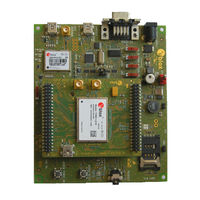
Ublox TOBY-L2 series User Manual (31 pages)
LTE/DC-HSPA+/EGPRS Cellular Evaluation Kits
Brand:
Ublox
| Category:
Motherboard
| Size: 2 MB
Table of Contents
Contents
3
Table of Contents
3
Starting up
4
EVK-L2 Overview
4
EVK-L2 Block Diagram
7
Switches, Jumpers and Buttons
8
Leds
8
Connectors
9
EVK-L2 Pin out
10
EVK-L2 for TOBY-L2 Series Modules, Product Version "01
10
EVK-L2 for TOBY-L2 Series Modules, Product Versions "02" / "62" Onwards
12
Software Installation
13
Board Setup
14
Enabling Error Result Codes
15
PIN Code Insertion (When Required)
15
Registration on a Cellular Network
16
Enable Audio Codec Configuration to Provide Voice Capability
16
Switching off the EVK-L2
16
Appendix
17
A Setting up at Terminal Applications for Communication with EVK-L2
17
BEVK-L2 Setup for Internet Browsing (Windows)
18
CEVK-L2 Setup for Internet Browsing (Linux)
22
D Optimal Throughput
25
E Examples of at Commands
26
Enable Communication between Cellular and Wi-Fi Module
26
F Current Consumption Measurement
27
EVK-L2 for TOBY-L2 Modules, Product Version "01
27
EVK-L2 for TOBY-L2 Modules, Product Versions "02"/ "62" Onwards
28
Declaration of Conformities
29
Related Documents
29
Revision History
29
Contact
30
Advertisement
Related Products
Ublox TOBY-L200 Series
Ublox TOBY-L201 Series
Ublox TOBY-L210 Series
Ublox TOBY-L220 Series
Ublox TOBY-L280 Series
Ublox TOBY-L200-00S-00
Ublox TOBY-L200-00S-01
Ublox TOBY-L200-02S-00
Ublox TOBY-L200-03A-01
Ublox TOBY-L200-02S-01
UBlox Categories
Control Unit
Motherboard
Computer Hardware
Wireless modules
Receiver
More UBlox Manuals
Login
Sign In
OR
Sign in with Facebook
Sign in with Google
Upload manual
Upload from disk
Upload from URL