Table of Contents
Advertisement
Quick Links
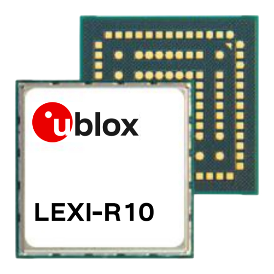
LEXI-R10 series
LTE Cat 1bis modules
System integration manual
Abstract
This document describes the features and the integration of the ultra-small LEXI-R10 series cellular
modules. These modules are a complete and cost-efficient solution offering multi-band LTE Cat 1bis
data transmissions in the ultra-compact LEXI form factor.
UBX-23008149 - R04
C1-Public
LEXI-R10
www.u-blox.com
Advertisement
Table of Contents


Need help?
Do you have a question about the LEXI-R10 Series and is the answer not in the manual?
Questions and answers