
Related Manuals for Dialog Semiconductor DA14695 USB Kit


Summary of Contents for Dialog Semiconductor DA14695 USB Kit
-
Page 1: Abstract
User Manual DA14695 USB Kit UM-B-103 Abstract This document outlines the system design, configuration options, and supported features of DA14695 USB Kit, rev-C (331-22-C). -
Page 2: Table Of Contents
UM-B-103 DA14695 USB Kit Contents Abstract ..............................1 Contents ............................... 2 Figures ..............................3 Tables ..............................3 Terms and Definitions ........................4 References ............................. 4 Introduction ............................ 5 System Overview ........................... 5 Features ..........................5 System and Components Description (Top View) ..............6 System and Components Description (Bottom View) ............ -
Page 3: Figures
DA14695 USB Kit Figures Figure 1: DA14695 USB Kit ........................5 Figure 2: DA14695 USB Kit - Top Side ....................6 Figure 3: DA14695 USB Kit - Bottom Side .................... 7 Figure 4: Test Points Topology (BOTTOM View) .................. 9 Figure 5: Block Diagram of DA14695 USB Kit .................. -
Page 4: Terms And Definitions
UM-B-103 DA14695 USB Kit Terms and Definitions Communication Interface Board Direct Current Resistor DMIPS Dhrystone Million Instructions per Second GPIO General Purpose Input Output Inter-Integrated Circuit JTAG Join Test Action Group Low Dropout MISO Master In Slave Out MOSI Master Out Slave In... -
Page 5: Introduction
DA14695 USB Kit Introduction This document describes the DA14695 USB Kit. This kit offers a low-cost development board with basic functionality. The development kit is implemented on a single PCB. The block diagram, the actual board, the various sections and settings as well as the connectivity are presented. The purpose of this cost-effective USB kit is to provide users with the capability of: ●... -
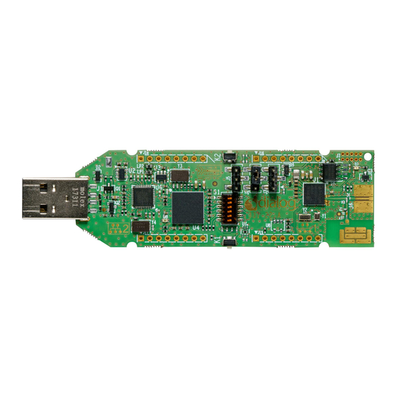
Page 6: System And Components Description (Top View)
UM-B-103 DA14695 USB Kit System and Components Description (Top View) Figure 2: DA14695 USB Kit - Top Side The USB kit is based on the DA14695 SoC in an VFBGA86 package. The marked and numbered sections of the system are:... -
Page 7: System And Components Description (Bottom View)
System and Components Description (Bottom View) Figure 3: DA14695 USB Kit - Bottom Side The bottom side of DA14695 USB kit provides information about the MikroBUS™ pins assignment, the SEGGER ID, and the date code. Test points have been placed for monitoring various signal behaviors and voltage levels of the components. -
Page 8: Test Points
UM-B-103 DA14695 USB Kit Test Points Test points have been placed on the bottom side of the board and allow users to have access to signals and I/Os, or measure supplies voltage levels. Table 1 shows the assignment for each test... -
Page 9: Figure 4: Test Points Topology (Bottom View)
UM-B-103 DA14695 USB Kit Test Point Assigned to Comments TP33 SWO/TDO For programming U4 in production - Not used for development TP34 DBLED Voltage level for Green LED TP35 SWO/TDO For programming U4 in production - Not used for development... -
Page 10: Block Diagram
Antenna LED (D7) & 32MHz 32KHz Push button (K1) Figure 5: Block Diagram of DA14695 USB Kit The power of Dialog’s DA14695 SoC on the USB kit can be supplied from three different sources (Figure ● Default configuration: 5 V provided to VBUS pin, when jumper placed to J2 header (pin 2-3) ●... -
Page 11: Usb Kit System
UM-B-103 DA14695 USB Kit USB Kit System Overview ● Board name/number: ○ DA14695 USB Kit/331-22-C ● SoC: ○ DA14695 in a VFBGA86 package ● Flash memory: ○ MX25U3235F (32 Mbit) QSPI Flash Memory, 8-pin SOIC (200 mil) package ○ 1.8 V (V18P to pin V18F) power supply (default) ●... -
Page 12: Figure 6: Da14695 Schematic
UM-B-103 DA14695 USB Kit Figure 6: DA14695 Schematic The DA14695 SoC power management subsystem consists of: ● VBUS: battery charger input as well as USB bus voltage ○ A decoupling capacitor (C2, 0402 package, 6.3 V) equal or less than 4.7 μF is placed close to VBUS pin ●... - Page 13 UM-B-103 DA14695 USB Kit ○ V30 is the default option for GPIO voltage levels (expect for the QSPI-RAM I/Os which are fixed to 1.8 V) ○ The current delivery capability of the V30 power rail is 150 mA ○ Overcurrent protection circuit limits the current on V30 if an external device misbehaves ●...
-
Page 14: Da14695 Pin Assignment
UM-B-103 DA14695 USB Kit DA14695 Pin Assignment Most of the available signals are utilized or extracted on the breakout connectors. Table 2 provides the pin assignment of the breakout connectors on the USB kit and the related pin name on the VFBGA86 package of the DA14695. - Page 15 UM-B-103 DA14695 USB Kit AQFN60 Pin Development Kit Signal Header Comments Name GPIO/MikroBUS™ Universal Asynchronous P0_29 GPIO/MB1_TX J16.4 Transmitter (slot 1) GPIO/MikroBUS™ I2C SCL (slot 1) P0_30 GPIO/MB1_SCL J16.5 GPIO/MikroBUS™ I2C SDA (slot 1) P0_31 GPIO/MB1_SDA J16.6 P1_00 J4.3 UART interface GPIO/MikroBUS™...
-
Page 16: Booting From Uart
UM-B-103 DA14695 USB Kit Booting from UART There is only one boot loader option for booting from UART using pins P0_9 (T_TX) and P0_8 (T_RX). Please note that UART-booting does not support hardware handshake signals (RTS/CTS). The settings for UART booting are: ●... -
Page 17: Antenna And Rf Port
A printed type antenna is currently used as the default antenna in the DA14695 USB Kit. The DA14695 USB Kit provides a single-ended RFIO port matched to 50 Ω. The RF port consists of the RFIOp, RFIOm, and RFIOm2 pins, of which RFIOm and RFIOm2 are connected to ground. A copper trace with an impedance of 50 Ω... -
Page 18: Qspi Data Flash Memory (U5)
SPI as well as 2-clock instruction cycle Quad Peripheral Interface (QPI), Serial Clock, Chip Select, Serial Data I/O0 (DI), I/O1(D0), I/O2 (/WP), and I/O3(/HOLD). The selected QSPI flash for the DA14695 USB Kit is MX25U3235FM2I-10G in 8-pin SOIC 208mil package (U5). DA14695 USB Kit can support QSPI Data flash with 8-pin SOIC 150mil package... -
Page 19: Reset Circuit
DA14695 USB Kit Reset Circuit Figure 11: Reset Circuit The DA14695 comprises an RSTn pad which is active low. The DA14695 USB Kit can be reset by pressing the on-board RESET push button (K2, Figure 12) or through software from the UART &... -
Page 20: 5.10 Debugging Port Dip Switch
UM-B-103 DA14695 USB Kit Figure 14: General Purpose Push Button K1 (Populated at TOP) 5.10 Debugging Port DIP Switch Figure 15: Debugging DIP Switch S1 is a DIP switch which allows users to disconnect the pins used for debugging (default state is all pins connected) to allow accurate deep sleep power measurement. -
Page 21: 5.11 User Controlled Led
Figure 19: Mikrobus™ Pin Assignment MikroBUS™ The DA14695 USB Kit can support modules. Users must place and solder J15, J16 sockets (for slot #1) and/or J17, J18 sockets (for slot #2) on the top side of the board as shown in Figure 20. -
Page 22: Figure 20: J15, J16, J17, And J18 Female Sockets (Must Be Soldered By Users)
MikroBus™ standard guideline for add-on board insertion. For more information, please check specifications. The pin assignment is printed at the bottom side of the DA14695 USB Kit (Figure 22). -
Page 23: 5.13 Gnd Test Point
Figure 24: GND Support Point (Must Be Placed by Users) 5.14 Over Voltage Protection Circuit (OVP) The DA14695 USB Kit can be used as a portable standalone device. The power supply can be a power-bank or a mobile charger. The overvoltage protection circuit OVP circuit can protect the device from overvoltage of up to 20 V. -
Page 24: 5.15 Over-Current Protection Circuit On V30 Power Rail
UM-B-103 DA14695 USB Kit 5.15 Over-Current Protection Circuit on V30 Power Rail A P-FET is added in series with V30 power rail to prevent the voltage on the pin from dropping to very low levels if a peripheral surge sets an overcurrent condition. -
Page 25: Debugging Processor (U4)
UM-B-103 DA14695 USB Kit 5.17 Debugging Processor (U4) Two debugging options (JTAG/UART) are available on the DA14695 SoC. The USB-to-JTAG and USB-to-UART functions are implemented by the SAM3U2CA processor (U4) (Figure 28), running the Segger JLink-OB firmware. The functions served by U4 are: ●... -
Page 26: 5.18 Power Section
UM-B-103 DA14695 USB Kit 5.18 Power Section The DA14695 USB Kit is supplied from 5 V to VBUS pin via J2 header (jumper has been placed to connect pins 2-3). Figure 29 shows the power tree. 3V3D Segger 3.3V LDO_EN... -
Page 27: 5.19 Power Selection Headers
UM-B-103 DA14695 USB Kit 5.19 Power Selection Headers The DA14695 USB Kit allows users to power supply the DA14695 from three different sources: ● 5 V to VBUS pin (default) ● 3.3 V to VBAT pin (optional) ● 3.6 V to 4.2 V from external battery to VBAT pin (optional) The default power configuration for DA14695 is from VBUS 5 V via power selection header J2. -
Page 28: Pcb Layout
UM-B-103 DA14695 USB Kit PCB Layout Dimensions: 100 mm × 26.5 mm × 11 mm Number of layers: 4 PCB thickness: 1.55 mm Material: FR-4 Solder mask TOP/BOTTOM: Green Silkscreen TOP/BOTTOM: White Surface finish: Che Ni/Au Figure 31: PCB Cross Section The total thickness of the board is 1.55 mm. -
Page 29: Appendix A Schematics
UM-B-103 DA14695 USB Kit Appendix A Schematics Figure 32: DA14695 SoC Section User Manual Revision 1.0 14-Feb-2019 CFR0012 29 of 34 © 2019 Dialog Semiconductor... -
Page 30: Figure 33: Uart & Jtag Interface Chip Section
UM-B-103 DA14695 USB Kit Figure 33: UART & JTAG Interface Chip Section User Manual Revision 1.0 14-Feb-2019 CFR0012 30 of 34 © 2019 Dialog Semiconductor... -
Page 31: Figure 34: Usb Hub Section
UM-B-103 DA14695 USB Kit Figure 34: USB Hub Section User Manual Revision 1.0 14-Feb-2019 CFR0012 31 of 34 © 2019 Dialog Semiconductor... -
Page 32: Appendix B Bill Of Materials
UM-B-103 DA14695 USB Kit Appendix B Bill of Materials Figure 35: Bill of Materials (BOM) User Manual Revision 1.0 14-Feb-2019 CFR0012 32 of 34 © 2019 Dialog Semiconductor... -
Page 33: Revision History
UM-B-103 DA14695 USB Kit Revision History Revision Date Description 14-Feb-2019 Initial version. User Manual Revision 1.0 14-Feb-2019 CFR0012 33 of 34 © 2019 Dialog Semiconductor... - Page 34 Terms and Conditions of Sale, available on the company website (www.dialog-semiconductor.com) unless otherwise stated. Dialog and the Dialog logo are trademarks of Dialog Semiconductor plc or its subsidiaries. All other product or service names are the property of their respective owners.
Need help?
Do you have a question about the DA14695 USB Kit and is the answer not in the manual?
Questions and answers