Table of Contents
Advertisement
Quick Links
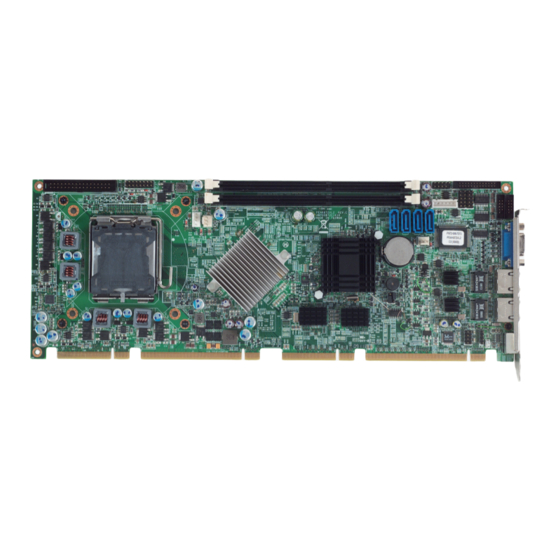
PEAK872VL2 Quick Reference Guide
JP8 Line out
PIN Description
PIN Description
1
LINEOUT_L
3
LINEOUT_JD
2
GND
4
LINEOUT_R
JP9 MIC in
PIN Description
PIN Description
1
MICIN_L
3
MICIN_JD
2
GND
4
MICIN_R
CN1 CPU FAN
PIN Description
PIN Description
1
GND
3
NC
2
+12V
4
ICH_PWM
FAN1/FAN2 SYSTEM FAN1/FAN2
PIN Description
PIN Description
1
ICH_PWM
3
Sense
2
+12V
CN2/CN3/CN4/CN5
SATA0/SATA1/ SATA2/SATA3
PIN Description
PIN Description
1
GND
5
SATA_RXN
2
SATA_TXP
6
SATA_RXP
3
SATA_TXN
7
GND
4
GND
Ver A. (P/N:60177A0140X00)
JP3 AT/ATX Power type select
PIN Description
1-2 AT
JP3 RTC clear
PIN Description
1-2 NORMAL
J6 USB 0/1 Connector
PIN Description
1
+5VSB
2
Data 0-
3
Data 0+
J9/J10 COM 1/ COM 2 connector
PIN Description
1
DCD
2
RXD
3
TXD
4
DTR
5
GND
JP7 Line in
PIN Description
1
LINEIN_L
2
GND
JP1 IDE LED/ POWER LED / POWER ON / RESET / SM BUS /
System thermal
PIN Description
PIN Description
1
+5V
9
+5V
2
+5V
10 SMB_ Data
3
IDE_LED
11
GND
4
GND
12 SMB_ Clock
5
Power ON
13 GND
6
GND
14 Thermal Pin
7
Reset
15 Speaker
8
GND
16 Thermal GND
PIN Description
2-3 ATX
PIN Description
2-3 Clear CMOS
PIN Description
4
Data 1-
5
Data 1+
6
GND
PIN Description
6
DSR
7
RTS
8
CTS
9
RI
10
NC
PIN Description
3
LINEIN JD
4
LINEIN_R
Advertisement
Table of Contents

Subscribe to Our Youtube Channel
Related Manuals for Nexcom PEAK872VL2


Summary of Contents for Nexcom PEAK872VL2
- Page 1 PEAK872VL2 Quick Reference Guide Ver A. (P/N:60177A0140X00) JP3 AT/ATX Power type select PIN Description PIN Description 1-2 AT 2-3 ATX JP3 RTC clear PIN Description PIN Description 1-2 NORMAL 2-3 Clear CMOS J6 USB 0/1 Connector PIN Description PIN Description...
- Page 2 JP5 Keyboard Lock JP8 PIO connector J1 Floppy Connector PIN Description PIN Description PIN Description PIN Description PIN Description PIN Description Line Print 14 Auto Feed# Keyboard Lock 18 DIR# Strobe DENSEL# 19 GND Parallel Data 0 15 Error# 20 STEP# Parallel Data 1 16 Initialize# JP6 IR 21 GND...
Need help?
Do you have a question about the PEAK872VL2 and is the answer not in the manual?
Questions and answers