Advertisement
Quick Links
DESCRIPTION
Demonstration circuit 1726 is a dual high efficiency
monolithic step-down (buck) DC/DC switching regulator
designed for double-data-rate (DDR) memory termina-
tion in computer systems. The VDDQ output is capable
of sourcing and sinking up to 3A with output voltages of
1.5V, 1.8V, 2.5V plus an optional voltage, selected using
jumpers. The VTT output can also source and sink up
to 3A with an output voltage equal to half of the VDDQ
voltage, half of the input voltage or half of an externally
applied voltage, selected using a jumper. An additional low
current output (VTTR) equal to the VTT voltage capable of
sourcing and sinking up to 10mA is included. Input voltage
range is from 2.25V to 5.5V with overvoltage protection
for transients exceeding 6.5V. Switching frequency is set
to 1MHz although it can be programmed up to 4MHz and
can be synchronized to an external clock for noise sensi-
tive applications.
Jumpers are included for selecting either internal or exter-
nal compensation and jumpers for low quiescent current
shutdown for each regulator. Other jumpers allow select-
ing internal or external soft-start, selecting the switching
PERFORMANCE SUMMARY
PARAMETERS
Input Voltage Range (VIN)
VDDQ Output Voltages (1.5V, 1.8V, 2.5V)
VTTR Output Voltage
VTT Output Voltage
Load Regulation (Each Regulator)
Maximum Output Current (Each Regulator)
Switching Frequency
Output Voltage Ripple
Efficiency
Efficiency
DEMO MANUAL DC1726
Dual ±3A Synchronous Buck
Regulator for DDR Termination
phase between the two regulators and selecting external
frequency synchronizing, and forced continuous or pulse
skipping modes of operation for the VDDQ regulator only.
Terminals are provided for connecting an input supply,
output loads and voltmeters. Other terminals include
external sync input, external reference input, external
tracking input, and separate power good outputs that
pull low at start-up and when the VDDQ or VTT output is
outside a voltage window.
The LTC
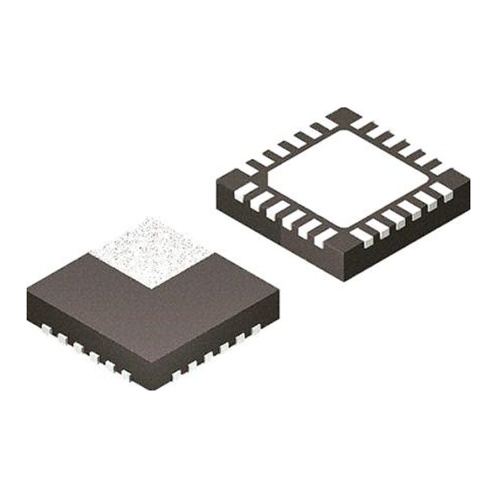
®
3618 used on this board is housed in a 24-pin 4mm
× 4mm thermally enhanced QFN package. The LTC3618
is also available in a 24-pin TSSOP package.
The LTC3618 data sheet gives a complete description of
the part, operation and application information and should
be read in conjunction with this quick start guide.
Design files for this circuit board are available at
http://www.linear.com/demo
L, LT, LTC, LTM, μModule, Linear Technology and the Linear logo are registered trademarks of
Linear Technology Corporation. All other trademarks are the property of their respective owners.
(T
= 25°C)
A
CONDITION
VIN = 3.3V
VIN = 3.3V
VIN = 3.3V
VIN = 3.3V, 0 to 3A Load
VIN = 3.3V
VIN = 3.3V, 0 to 3A Load
VIN = 3.3V, VDDQ = 1.8V, 2A Load
VIN = 3.3V, VTT = 900mV, 2A Load
LTC3618EUF
TYPICAL VALUE
2.25V to 5.5V
±2.5%
VDDQIN • 0.5 ±2%
VTTR ±6mV
5mV
±3A
1MHz ±20%
10mV
P-P
88%
80.5%
dc1726f
1
Advertisement

Related Manuals for Linear Technology LTC3618EUF


Summary of Contents for Linear Technology LTC3618EUF
- Page 1 L, LT, LTC, LTM, μModule, Linear Technology and the Linear logo are registered trademarks of shutdown for each regulator. Other jumpers allow select- Linear Technology Corporation. All other trademarks are the property of their respective owners.
-
Page 2: Quick Start Procedure
DEMO MANUAL DC1726 QUICK START PROCEDURE Demonstration circuit 1726 allows the user to quickly 7. Verify that the VTT output voltage is equal to the VTTR evaluate the performance of the LTC3618. Refer to Figure 2 voltage ±6mV. The error voltage can be read differentially for proper measurement equipment setup and follow the by placing the meter leads between the VTTR and VTT procedure below... - Page 3 DEMO MANUAL DC1726 QUICK START PROCEDURE VIN - VTT Connection for VTT Sinking Current = –––––––– sinking LOAD = ––––– sourcing LOAD Sourcing 10W Load 5V @ 5A Resistor Input Power Supply (set to 3.3V) VDDQ Output Output VTTR Output Figure 2.
- Page 4 RES., CHIP , 845k, 1/16W, 1% 0603 VISHAY, CRCW0603845KFKEA RES., CHIP , 562k, 1/16W, 1% 0603 VISHAY, CRCW0603562KFKEA IC., LTC3618EUF UF-24 LINEAR TECH., LTC3618EUF#PBF Additional Demo Board Circuit Components C1, C2, CFFW1 CAP ., C0G, 10pF , 25V, 20% 0603 AVX, 06033A100MAT2A CAP ., X7R, 0.1μF , 50V, 20% 0603...
-
Page 5: Schematic Diagram
Information furnished by Linear Technology Corporation is believed to be accurate and reliable. However, no responsibility is assumed for its use. Linear Technology Corporation makes no representa- tion that the interconnection of its circuits as described herein will not infringe on existing patent rights. - Page 6 Linear Technology Corporation (LTC) provides the enclosed product(s) under the following AS IS conditions: This demonstration board (DEMO BOARD) kit being sold or provided by Linear Technology is intended for use for ENGINEERING DEVELOPMENT OR EVALUATION PURPOSES ONLY and is not provided by LTC for commercial use. As such, the DEMO BOARD herein may not be complete in terms of required design-, marketing-, and/or manufacturing-related protective considerations, including but not limited to product safety measures typically found in finished commercial goods.
Need help?
Do you have a question about the LTC3618EUF and is the answer not in the manual?
Questions and answers