Table of Contents
Advertisement
Quick Links
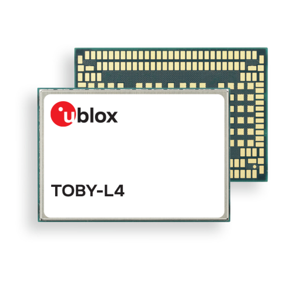
TOBY-L4 series
LTE Advanced (Cat 6) modules
with 3G and 2G fallback
System Integration Manual
Abstract
This document describes the features and the system integration of
TOBY-L4 series multi-mode cellular modules.
The modules are a complete and cost efficient LTE-FDD, LTE-TDD,
DC-HSPA+, (E)GPRS multi-mode and multi-band solution with uCPU
embedded Linux programming capability. The modules offer up to
301.5 Mb/s download and up to 51.0 Mb/s upload data rates with
Category 6 LTE-Advanced carrier aggregation technology in the
compact TOBY form factor.
www.u-blox.com
UBX-16024839 - R04
Advertisement
Table of Contents

Related Manuals for u-blox TOBY-L4 Series


Summary of Contents for u-blox TOBY-L4 Series
- Page 1 System Integration Manual Abstract This document describes the features and the system integration of TOBY-L4 series multi-mode cellular modules. The modules are a complete and cost efficient LTE-FDD, LTE-TDD, DC-HSPA+, (E)GPRS multi-mode and multi-band solution with uCPU embedded Linux programming capability. The modules offer up to 301.5 Mb/s download and up to 51.0 Mb/s upload data rates with...
- Page 2 The information contained herein is provided “as is” and u-blox assumes no liability for the use of the information. No warranty, either express or implied, is given, including but not limited, with respect to the accuracy, correctness, reliability and fitness for a particular purpose of the information.
-
Page 3: Preface
Application Note: These documents provide guidelines and information on specific hardware and/or software topics on u-blox cellular modules. See Related documents for a list of Application Notes related to your Cellular Module. How to use this Manual The TOBY-L4 series System Integration Manual provides the necessary information to successfully design and configure the u-blox cellular modules. -
Page 4: Table Of Contents
TOBY-L4 series - System Integration Manual Contents Preface ..........................3 Contents ..........................4 System description ....................... 7 Overview .............................. 7 Architecture ............................10 Pin-out ............................... 12 Operating modes ..........................20 Supply interfaces ..........................22 1.5.1 Module supply input (VCC) ......................22 1.5.2... - Page 5 TOBY-L4 series - System Integration Manual 2.2.1 Module supply (VCC) ........................53 2.2.2 RTC back-up supply (V_BCKP) ..................... 66 2.2.3 Generic digital interfaces supply output (V_INT) ................67 System functions interfaces ........................ 68 2.3.1 Module power-on (PWR_ON) ...................... 68 2.3.2 Module reset (RESET_N) ......................
- Page 6 TOBY-L4 series - System Integration Manual 3.3.6 Wave soldering.......................... 123 3.3.7 Hand soldering .......................... 123 3.3.8 Rework ............................123 3.3.9 Conformal coating ........................123 3.3.10 Casting ............................123 3.3.11 Grounding metal covers ......................123 3.3.12 Use of ultrasonic processes ......................123 Approvals ........................
-
Page 7: System Description
AT commands described in the u-blox AT Commands Manual [2] TOBY-L4 series modules are the ideal product for the development of all kinds of automotive devices, such as smart antennas and in-dash telematics / infotainment devices, supporting a comprehensive set of HW interfaces (including RGMII/RMII for Ethernet and analog audio) over a very extended temperature range that allow the establishment of an emergency call up to +95 °C, complemented by a set of state-of-the art security features. - Page 8 TOBY-L4 series - System Integration Manual Table 1 summarizes the main features and interfaces of the TOBY-L4 series modules. Model Region Bands Interfaces Features Grade 2,4,5 North TOBY-L4006-00 7,12 4 1 1 2 1 1 1 2 2 14 2 ● ● ● ● ● ● ● ● ● ● ● ● ●...
- Page 9 Table 3: TOBY-L4 series supported bands and Carrier Aggregation combinations summary Down-Link Rx diversity not supported on this band TOBY-L4 series modules support all the E-UTRA channel bandwidths for each operating band according to 3GPP TS 36.521-1 [13]. UBX-16024839 - R04 System description...
-
Page 10: Architecture
V_INT (I/O) External reset Figure 1: TOBY-L4 series modules simplified block diagram TOBY-L4 series modules internally consist of the RF, Baseband and Power Management sections described herein with more details than the simplified block diagrams of Figure 1. RF section The RF section is composed of an RF transceiver, PAs, LNAs, crystal oscillator, filters, duplexers and RF switches. - Page 11 TOBY-L4 series - System Integration Manual Baseband and power management section The Baseband and Power Management section is composed of the following main elements: A mixed signal ASIC, which integrates Microprocessor for control functions DSP core for cellular Layer 1 and digital processing of Rx and Tx signal paths...
-
Page 12: Pin-Out
TOBY-L4 series - System Integration Manual Pin-out Table 4 lists the pin-out of the TOBY-L4 series modules, with pins grouped by function. Function Pin Name Pin No Description Remarks Power 70,71,72 Module supply input VCC supply circuit affects the RF performance and compliance of the device integrating the module with applicable required certification schemes. - Page 13 TOBY-L4 series - System Integration Manual Function Pin Name Pin No Description Remarks SIM0 VSIM VSIM = 1.8 V / 3 V output as per the connected SIM type. SIM0 supply output See section 1.8 for functional description. See section 2.5 for external circuit design-in.
- Page 14 TOBY-L4 series - System Integration Manual Function Pin Name Pin No Description Remarks USB_SSTX+ 90 nominal differential characteristic impedance. USB Super-Speed 3.0 diff. transmitter (+) Internal series 100 nF capacitor for AC coupling. Compliant with USB Revision 3.0 specification [4].
- Page 15 TOBY-L4 series - System Integration Manual Function Pin Name Pin No Description Remarks UART1 RXD1 UART1 data output / 1.8 V output, Circuit 104 (RXD) in ITU-T V.24, SPI1 MOSI alternatively configurable as SPI1 MOSI by uCPU API. See section 1.9.2 / 1.9.3 for functional description.
- Page 16 TOBY-L4 series - System Integration Manual Function Pin Name Pin No Description Remarks I2C1 SCL1 I2C1 clock 1.8 V open drain. External pull-up required. See section 1.9.4 for functional description. See section 2.6.4 for external circuit design-in. SDA1 I2C1 data 1.8 V open drain.
- Page 17 TOBY-L4 series - System Integration Manual Function Pin Name Pin No Description Remarks ETH_RX_CLK Ethernet Receive RGMII: Receive reference clock (RXC). Clock RMII: Not used. See section 1.9.6 for functional description. See section 2.6.6 for external circuit design-in. ETH_RX_CTL Ethernet Receive...
- Page 18 TOBY-L4 series - System Integration Manual Function Pin Name Pin No Description Remarks MMC_RST_N Multi-Media Card Embedded Multi-Media / SD Card memory reset. Reset See section 1.10 for functional description. See section 2.7 for external circuit design-in. MMC_CD_N Multi-Media Card Embedded Multi-Media / SD Card detect.
- Page 19 47-49, 77, 84, See sections 1.14 and 2.11 91, 153-158, 163-167, 180, 181, 183-192, 194, 196-202, 224, 225, 242, 243, 244-246 Table 4: TOBY-L4 series module pin definition, grouped by function UBX-16024839 - R04 System description Page 19 of 143...
-
Page 20: Operating Modes
TOBY-L4 series - System Integration Manual Operating modes TOBY-L4 series modules have several operating modes. The operating modes are defined in Table 5 and described in detail in Table 6, providing general guidelines for operation. General Status Operating Mode Definition... - Page 21 Idle No RF Tx/Rx in progress, Any wake up event described Call terminated, in the module operating Communication dropped modes summary table above Figure 2: TOBY-L4 series modules operating modes transitions UBX-16024839 - R04 System description Page 21 of 143...
-
Page 22: Supply Interfaces
RGMII interface supply, V_MMC eMMC interface supply, and any other internal rail. During operation, the current drawn by the TOBY-L4 series modules through the VCC pins can vary by several orders of magnitude. This ranges from the pulse of current consumption during GSM transmitting bursts at maximum power level in connected mode (as described in section 1.5.1.2) to the low current consumption... - Page 23 VCC supply circuit compliant with the requirements listed in Table 7. The supply circuit affects the RF compliance of the device integrating TOBY-L4 series modules with applicable required certification schemes as well as antenna circuit design. Compliance is guaranteed if the requirements summarized in Table 7 are fulfilled.
- Page 24 TOBY-L4 series - System Integration Manual 1.5.1.2 VCC current consumption in 2G connected mode When a GSM call is established, the VCC module current consumption is determined by the current consumption profile typical of the GSM transmitting and receiving bursts.
- Page 25 TOBY-L4 series - System Integration Manual When a GPRS connection is established, more than one slot can be used to transmit and/or more than one slot can be used to receive. The transmitted power depends on the network conditions, which set the peak current consumption, but following the 3GPP specifications, the maximum Tx RF power is reduced if more than one slot is used to transmit, so the maximum peak of current is not as high as can be the case with a 2G single-slot call.
- Page 26 TOBY-L4 series - System Integration Manual 1.5.1.3 VCC current consumption in 3G connected mode During a 3G connection, the module can transmit and receive continuously due to the Frequency Division Duplex (FDD) mode of operation with the Wideband Code Division Multiple Access (WCDMA).
- Page 27 TOBY-L4 series - System Integration Manual 1.5.1.4 VCC current consumption in LTE connected mode During an LTE connection, the module can transmit and receive continuously due to the Frequency Division Duplex (FDD) mode of operation used in LTE radio access technology.
- Page 28 The power saving configuration is disabled by default, but it can be enabled using the AT+UPSV command (see the u-blox AT Commands Manual [2]) or the dedicated uCPU API. When power saving is enabled, the module automatically enters the low power idle mode whenever possible, reducing current consumption.
- Page 29 Power saving configuration is by default disabled. It can also be disabled using the AT+UPSV command (see the u-blox AT Commands Manual [2]) or the dedicated uCPU API. The module processor core is activated during idle mode, and the 26 MHz reference clock frequency is used. It would draw more current during the paging period than that in the power saving mode.
-
Page 30: Rtc Back-Up Supply (V_Bckp)
1.5.3 Generic digital interfaces supply output (V_INT) The V_INT output pin of the TOBY-L4 series modules is connected to an internal 1.8 V supply. This supply is internally generated by a switching step-down regulator integrated in the Power Management Unit and it is internally used to source the generic digital I/O interfaces of the cellular module, as illustrated in Figure 11. -
Page 31: System Function Interfaces
Figure 12: TOBY-L4 series PWR_ON input description TOBY-L4 series modules do not switch on by applying the VCC supply only: a low pulse must be forced on the PWR_ON pin when the VCC voltage is stable at its nominal value within the valid operating range. - Page 32 Before the TOBY-L4 series module is fully ready to operate, the host application processor should not send any AT command over the AT communication interface (USB) of the module.
-
Page 33: Module Power-Off
This abrupt emergency shutdown procedure is intended only for use for emergency, e.g. if the module does not provide a reply to a specific AT command after a time period longer than the one defined in the u-blox AT Commands Manual [2], or if shutdown via a normal switch-off procedure fails. - Page 34 TOBY-L4 series - System Integration Manual Figure 14 describes the TOBY-L4 series modules’ switch-off sequence started by means of the PWR_ON input pin, allowing storage of current parameter settings in the module’s non-volatile memory and a clean network detach, with the following phases ...
-
Page 35: Module Reset
An abrupt hardware reset occurs on TOBY-L4 series modules when a low level is applied on the RESET_N input pin. In this case, the current parameter settings are not saved in the module’s non-volatile memory and a clean network detach is not performed. -
Page 36: Antenna Interfaces
The ANT2 represents the secondary RF input for the reception of the RF signals for CA, MIMO and Rx diversity configurations supported by TOBY-L4 series modules as a required feature for LTE category 6 UEs. The ANT2 pin has a nominal characteristic impedance of 50 and must be connected to the secondary Rx antenna through a 50 ... - Page 37 The impedance of the antenna RF connection must match the 50 impedance of the ANT2 port. Frequency Range See the TOBY-L4 series Data Sheet [1] The required frequency range of the antennas connected to ANT2 port depends on the operating bands of the used cellular module and the used mobile network.
-
Page 38: Antenna Detection Interface (Ant_Det)
1.8.2 SIM detection interface The GPIO5 pin of TOBY-L4 series modules can be configured to detect the mechanical / physical presence of an external SIM card connected to the SIM0 interface. The pin can sense SIM card presence as intended to be properly connected to the mechanical switch of a SIM card holder as described in section 2.5:... -
Page 39: Data Communication Interfaces
SDIO interface , with the module acting as SDIO host, providing (see section 1.9.5): Communication with compatible u-blox short range radio modules by means of uCPU API Communication with external SDIO devices by means of uCPU API ... -
Page 40: Usb Interface
The USB High-Speed 2.0 host role is not supported by the "50" product versions. TOBY-L4 series modules include a USB Super-Speed 3.0 compliant interface, supporting up to 5 Gbit/s data rate, and also including a USB High-Speed 2.0 compliant interface, supporting up to 480 Mbit/s data rate. -
Page 41: Uart Interfaces
USB_SSTX+/USB_SSTX–, USB Super-Speed differential transmitter data lines USB_SSRX+/USB_SSRX–, USB Super-Speed differential receiver data lines USB drivers are available for Windows operating system platforms. TOBY-L4 series modules are compatible with standard Linux/Android USB kernel drivers. 1.9.2 UART interfaces UART interfaces are not supported by the "50" product version, except for trace logging (diagnostic purposes) and Ring Indicator functionality over the UART0 interface. - Page 42 The RI line can additionally notify URCs and/or incoming data, if the feature is enabled by the specific AT+URING command (for more details, see the u-blox AT Commands Manual [2]): the RI line is asserted when one of the configured events occur and it remains asserted for 1 s unless another configured event will happen, with the same behavior illustrated in Figure 18.
- Page 43 TOBY-L4 series - System Integration Manual 1.9.2.2 UART1 interface The UART1 Universal Asynchronous Receiver/Transmitter serial interface, with CMOS compatible signal levels (0 V for ON / active state and 1.8 V for OFF / idle state), can operate as a ...
-
Page 44: Spi Interfaces
TOBY-L4 series - System Integration Manual 1.9.3 SPI interfaces SPI interfaces are not supported by the "50" product version. 1.9.3.1 SPI0 interface The SPI0 1.8 V Serial Peripheral Interface supports communication with an external SPI slave devices, with the module acting as SPI master, by means of the uCPU API, with the following pins: ... -
Page 45: Ddc (I C) Interfaces
GNSS receiver. The modules provide embedded GNSS aiding that is a set of specific features developed by u-blox to improve the cellular / GNSS system power consumption and the GNSS performance, decreasing the Time-To-First-Fix (TTFF), thus allowing to calculate the position in a shorter time with higher accuracy. -
Page 46: Rgmii Interface
RGMII interface is not supported by the "50" product version. TOBY-L4 series modules include an Ethernet Media Access Control (MAC) block supporting up to 1 Gbit/s data rate via a Reduced Gigabit Media-Independent Interface compliant with the RGMII Version 1.3 specification [7] and the RMII Revision 1.2 specification [8]. -
Page 47: Emmc Interface
1.10 eMMC interface The eMMC interface is not supported by the "50" product version. TOBY-L4 series modules include a 4-bit embedded Multi-Media Card interface compliant with the JESD84-B451 Embedded Multimedia Card (eMMC) Electrical Standard 4.51 [9]. The following signals are provided for connection and management of an external eMMC / SD memory by means of the uCPU API: ... -
Page 48: Audio Interfaces
TOBY-L4 series - System Integration Manual 1.11 Audio interfaces 1.11.1 Analog audio interfaces TOBY-L4 series modules provide the following analog audio interfaces: Analog audio inputs (analog audio uplink path) First differential analog audio input (MIC1_P, MIC1_N), which can be connected to the output of an external analog audio device, or an external microphone for voice call or eCall purposes. -
Page 49: Digital Audio Interface
TOBY-L4 series - System Integration Manual 1.11.2 Digital audio interface TOBY-L4 series modules include two 4-wire I S digital audio interfaces: I2S0 digital audio interface, consisting of the following pins: I2S_TXD data output I2S_RXD data input ... -
Page 50: Adc Interfaces
1.12 ADC interfaces The ADC pins are not supported by the "50" product version. TOBY-L4 series modules include Analog to Digital Converter inputs (ADC1, ADC2), which can be handled by means of the dedicated uCPU API. 1.13 General Purpose Input/Output TOBY-L4 series modules "00"... -
Page 51: Reserved Pins (Rsvd)
Table 12: TOBY-L4 series modules "50" product versions GPIO custom functions summary 1.14 Reserved pins (RSVD) TOBY-L4 series modules have pins reserved for future use, marked as RSVD: they can all be left unconnected on the application board, except ... -
Page 52: Design-In
The following list provides a rank of importance in the application design, starting with the most significant: 1. Module antenna connection: Antenna circuit directly affects the RF compliance of the device integrating a TOBY-L4 series module with applicable certification schemes. Very carefully follow the suggestions provided in section 2.4 for the schematic and layout design. -
Page 53: Supply Interfaces
The switching step-down regulator is the typical choice when the available primary supply source has a nominal voltage much higher (e.g. greater than 5 V) than the operating supply voltage of TOBY-L4 series. The use of switching step-down provides the best power efficiency for the overall application and minimizes current drawn from the main supply source. - Page 54 The usage of a regulator or a battery not able to support the highest peak of VCC current consumption specified in the TOBY-L4 series Data Sheet [1] is generally not recommended. However, if the selected regulator or battery is not able to support the highest peak current of the module, it must be able to support with adequate margin at least the highest averaged current consumption value specified in the TOBY-L4 series Data Sheet [1].
- Page 55 TOBY-L4 series - System Integration Manual Figure 20 and Table 13 show an example of a high reliability power supply circuit, where the module VCC input is supplied by a step-down switching regulator capable of delivering maximum current with low output ripple and with fixed switching frequency in PWM mode operation greater than 1 MHz.
- Page 56 TOBY-L4 series - System Integration Manual Figure 21 and the components listed in Table 14 show an example of a low-cost power supply circuit, where the VCC module supply is provided by a step-down switching regulator capable of delivering to VCC pins the specified maximum peak / pulse current, transforming a 12 V supply input.
- Page 57 TOBY-L4 series - System Integration Manual 2.2.1.3 Guidelines for VCC supply circuit design using a Low Drop-Out linear regulator The use of a linear regulator is suggested when the difference from the available supply rail source and the VCC value is low. The linear regulators provide high efficiency when transforming a 5 VDC supply to a voltage value within the module VCC normal operating range.
- Page 58 TOBY-L4 series - System Integration Manual Figure 23 and the components listed in Table 16 show an example of a low-cost power supply circuit, where the VCC module supply is provided by an LDO linear regulator capable of delivering the specified highest peak / pulse current, with suitable power handling capability.
- Page 59 VCC pins must be capable of delivering a pulse current as the maximum peak current consumption during Tx burst at the maximum Tx power specified in the TOBY-L4 series Data Sheet [1] and must be capable of extensively delivering a DC current as the maximum average current consumption as specified in the TOBY-L4 series Data Sheet [1].
- Page 60 GSM call (when current consumption on the VCC supply can rise up as specified in the TOBY-L4 series Data Sheet [1]), place a bypass capacitor with large capacitance (at least 100 µF) and low ESR near the VCC pins, for example: ...
- Page 61 Guidelines for the external battery charging circuit TOBY-L4 series modules do not have an on-board charging circuit. Figure 25 provides an example of a battery charger design which is suitable for applications that are battery powered with a Li-Ion (or Li-Polymer) cell.
- Page 62 TOBY-L4 series - System Integration Manual 2.2.1.8 Guidelines for external battery charging and power path management circuit Application devices where both a permanent primary supply / charging source (e.g. ~12 V) and a rechargeable back-up battery (e.g. 3.7 V Li-Pol) are available at the same time as possible supply source should implement a suitable charger / regulator with integrated power path management function to supply the module and the whole device while simultaneously and independently charging the battery.
- Page 63 TOBY-L4 series - System Integration Manual Battery charging is managed in three phases: Pre-charge constant current (active when the battery is deeply discharged): the battery is charged with a low current, set to 10% of the fast-charge current. ...
- Page 64 Guidelines for removing VCC supply As described in section 1.6.2 and Figure 14, the VCC supply can be removed after the end of the TOBY-L4 series module’s internal power-off sequence, which must be properly started as described in section 1.6.2.
- Page 65 RF signal. This is more likely to happen with switching DC-DC converters, in which case it is better to select the highest operating frequency for the switcher and add a large L-C filter before connecting to the TOBY-L4 series modules in the worst case. ...
-
Page 66: Rtc Back-Up Supply (V_Bckp)
The internal regulator for V_BCKP is optimized for low leakage current and very light loads. Do not apply loads which might exceed the limit for the maximum available current from V_BCKP supply, as this can cause malfunctions in the module. The TOBY-L4 series Data Sheet [1] describes the detailed electrical characteristics. -
Page 67: Generic Digital Interfaces Supply Output (V_Int)
2.2.3 Generic digital interfaces supply output (V_INT) 2.2.3.1 Guidelines for V_INT circuit design TOBY-L4 series provide the V_INT generic digital interfaces 1.8 V supply output, which can be mainly used to: Indicate when the module is switched on (as described in sections 1.6.1, 1.6.2) ... -
Page 68: System Functions Interfaces
Guidelines for PWR_ON circuit design TOBY-L4 series PWR_ON input is equipped with an internal active pull-up resistor to an internal 1.3 V supply rail as illustrated in Figure 30: an external pull-up resistor is not required and should not be provided. -
Page 69: Module Reset (Reset_N)
2.3.2.1 Guidelines for RESET_N circuit design TOBY-L4 series RESET_N line is equipped with an internal pull-up to the V_INT supply as illustrated in Figure 31. An external pull-up resistor is not required. If connecting the RESET_N input to a push button, the pin will be externally accessible on the application device. -
Page 70: Module / Host Configuration Selection
2.3.3.1 Guidelines for HOST_SELECTx circuit design TOBY-L4 series modules include two 1.8 V digital pins (HOST_SELECT0, HOST_SELECT1), which can be configured for External Interrupt detection or as GPIO by means of the uCPU API: the pins can be connected to external devices following the guidelines provided in section 2.10. -
Page 71: Antenna Interface
RF compliance of the device integrating TOBY-L4 series modules with all the applicable required certification schemes depends on the antenna radiating performance. - Page 72 TOBY-L4 series - System Integration Manual Radiation performance depends on the whole PCB and antenna system design, including product mechanical design and usage. Antennas should be selected with optimal radiating performance in the operating bands according to the mechanical specifications of the PCB and the whole product.
- Page 73 TOBY-L4 series - System Integration Manual Guidelines for RF transmission line design Any RF transmission line, such as the ones from the ANT1 and ANT2 pads up to the related antenna connector or up to the related internal antenna pad, must be designed so that the characteristic impedance is as close as possible to 50 .
- Page 74 TOBY-L4 series - System Integration Manual the dielectric constant of the dielectric material (e.g. dielectric constant of the FR-4 dielectric material in Figure 33 and Figure 34) the gap from the transmission line to the adjacent ground plane on the same layer of the transmission line (e.g.
- Page 75 TOBY-L4 series - System Integration Manual Guidelines for RF termination design RF terminations must provide a characteristic impedance of 50 as well as the RF transmission lines up to the RF terminations themselves, to match the characteristic impedance of the ANT1 / ANT2 ports of the modules.
- Page 76 TOBY-L4 series - System Integration Manual Examples of antennas Table 24 lists some examples of possible internal on-board surface-mount antennas. Manufacturer Part Number Product Name Description Taoglas PA.710.A Warrior GSM / WCDMA / LTE SMD Antenna 698..960 MHz, 1710..2170 MHz, 2300..2400 MHz, 2490..2690 MHz 40.0 x 6.0 x 5.0 mm...
-
Page 77: Antenna Detection Interface (Ant_Det)
TOBY-L4 series - System Integration Manual 2.4.2 Antenna detection interface (ANT_DET) 2.4.2.1 Guidelines for ANT_DET circuit design Figure 36 and Table 27 describe the recommended schematic / components for the antennas detection circuit that must be provided on the application board and for the diagnostic circuit that must be provided on the antennas’... - Page 78 Values close to the measurement range maximum limit (approximately 50 k) or an open-circuit “over range” report (see the u-blox AT Commands Manual [2]) means that that the antenna is not connected or the RF cable is broken. ...
-
Page 79: Sim Interfaces
Guidelines for SIM cards, SIM connectors and SIM chips selection TOBY-L4 series modules provide two SIM interfaces for the direct connection of two external SIM cards/chips, which can be used alternatively (only one SIM at a time can be used for network access): ... - Page 80 A removable SIM card placed in a SIM card holder must be connected to the SIM0 or the SIM1 interface of TOBY-L4 series modules as illustrated in Figure 37, where the optional SIM detection feature is not implemented. Follow these guidelines to connect the module to a SIM connector without SIM presence detection: ...
- Page 81 TOBY-L4 series - System Integration Manual Guidelines for single SIM chip connection A solderable SIM chip (M2M UICC Form Factor) must be connected the SIM0 / SIM1 interface of TOBY-L4 series modules as illustrated in Figure 38. Follow these guidelines to connect the module to a solderable SIM chip without SIM presence detection: ...
- Page 82 If the optional SIM card detection feature is required by the application, then a removable SIM card placed in a SIM card holder must be connected to the SIM0 interface of TOBY-L4 series modules as illustrated in Figure 39: Follow these guidelines to connect the module to a SIM connector implementing SIM presence detection: ...
- Page 83 Two SIM cards / chips can be connected to the SIM interfaces of TOBY-L4 modules as illustrated in Figure 40. TOBY-L4 series modules do not support the usage of two SIMs at the same time, but two SIMs can be populated on the application board: ...
- Page 84 TOBY-L4 series - System Integration Manual FIRST SIM CARD TOBY-L4 series VPP (C6) VSIM VCC (C1) SIM_IO IO (C7) SIM_CLK CLK (C3) SIM_RST RST (C2) GND (C5) C2 C3 D1 D2 D3 D4 SECOND SIM CARD VPP (C6) VSIM1 VCC (C1)
-
Page 85: Guidelines For Sim Layout Design
VSIM1, SIM1_IO, SIM1_CLK, SIM1_RST for the SIM1 interface) may be critical if the SIM card is placed far away from the TOBY-L4 series modules or in close proximity to the RF antenna: these two cases should be avoided or at least mitigated as described below. -
Page 86: Data Communication Interfaces
GRM155R61A104KA01 - Murata D1, D2, D3 Very Low Capacitance ESD Protection PESD0402-140 - Tyco Electronics Table 32: Component for USB 2.0 interface application circuits, with TOBY-L4 series module acting as a USB device UBX-16024839 - R04 Design-in Page 86 of 143... - Page 87 Very Low Capacitance ESD Protection PESD0402-140 - Tyco Electronics DC/DC Boost Regulator Various Manufacturer Table 33: Component for USB 2.0 interface application circuits, with TOBY-L4 series module acting as a USB host USB 3.0 DEVICE USB 2.0 HOST TOBY-L4 series...
- Page 88 TOBY-L4 series - System Integration Manual 2.6.1.2 Guidelines for USB layout design The USB_D+/USB_D–, USB_SSTX+/USB_SSTX– and USB_SSRX+/USB_SSRX– lines require accurate layout design to achieve reliable signaling at the high speed data rates (up to 480 Mbit/s or up to 5 Gbit/s) supported by the USB 2.0 or USB 3.0 interface.
-
Page 89: Uart Interfaces
TOBY-L4 series - System Integration Manual 2.6.2 UART interfaces UART interfaces are not supported by the "50" product version, except for trace logging (diagnostic purposes) and Ring Indicator functionality over the UART0 interface. 2.6.2.1 Guidelines for UART circuit design 4-wire UART If RS-232 compatible signal levels are needed, the Maxim MAX13234E voltage level translator can be used. - Page 90 TOBY-L4 series - System Integration Manual 2-wire UART If the functionality of the CTSx and RTSx are not required in the application, or the lines are not available, then: Consider to connect the module RTSx input line to GND or to the CTSx output line of the module, since the module requires RTSx active (low electrical level) if HW flow-control is enabled If RS-232 compatible signal levels are needed, the Maxim MAX13234E voltage level translator can be used.
- Page 91 TOBY-L4 series - System Integration Manual Ring Indicator If a 1.8 V external Processor / Device is used, the Ring Indicator circuit should be implemented as illustrated in Figure 50. 1.8V Processor / Device TOBY-L4 series Figure 50: Ring Indicator application circuit to connect an external 1.8V processor / device If a 3.0 V external Processor / Device is used, then it is recommended to connect the 1.8 V Ring Indicator output...
- Page 92 TOBY-L4 series - System Integration Manual Additional considerations If a 3.0 V external Processor / Device is used, the voltage scaling from any 3.0 V output of the external Processor / Device to the corresponding 1.8 V input of the module can be implemented as an alternative low-cost solution, by means of an appropriate voltage divider.
-
Page 93: Spi Interfaces
2.6.3.1 Guidelines for SPI circuit design TOBY-L4 series modules include up to two 1.8 V Serial Peripheral Interfaces to communicate with external SPI slave devices, with the module acting as SPI master, by means of the uCPU API. Figure 52 describes a possible application circuit for the SPI0 interface, where two SPI slave devices are connected to the module using the two SPI0 Chip Select 0 (SPI_CS pin) and SPI0 Chip Select 1 (GPIO4 pin) to select the specific SPI slave device. -
Page 94: Ddc (I C) Interfaces
C bus specifications [6] regarding the rise and fall times of the signals. Figure 53 and Table 38 describe typical application circuits for connecting TOBY-L4 series modules to 1.8 V I2C devices (see Figure 53 top side) or 3 V I2C devices (see Figure 53 bottom side). - Page 95 TOBY-L4 series - System Integration Manual Connection with u-blox 1.8 V GNSS receivers Figure 54 shows an application circuit for connecting the cellular modules to a u-blox 1.8 V GNSS receiver. SDA / SCL pins of the cellular module are directly connected to the relative I C pins of the u-blox 1.8 V GNSS...
- Page 96 The supply of the u-blox 1.8 V GNSS receiver can be switched off using an external p-channel MOS controlled by the GPIO2 pin of the cellular modules by means of a suitable inverting transistor as shown in Figure 55, implementing the “GNSS supply enable”...
- Page 97 TOBY-L4 series - System Integration Manual Connection with u-blox 3.0 V GNSS receivers Figure 56 shows an application circuit for connecting the cellular modules to a u-blox 3.0 V GNSS receiver: As the SDA and SCL pins of the cellular module are not tolerant up to 3.0 V, the connection to the related C pins of the u-blox 3.0 V GNSS receiver must be provided using a suitable I...
-
Page 98: Sdio Interface
SDIO devices by means of the uCPU API Connection with u-blox short range radio communication modules Figure 58 and Table 43 show an application circuit for connecting TOBY-L4 series cellular modules to u-blox EMMY-W161 short range radio communication modules supporting IEEE 802.11a/b/g/n/ac data rates for Wi-Fi: ... - Page 99 Connection with external SDIO devices Figure 58 and Table 43 show an application circuit example for connecting the SDIO interface of TOBY-L4 series modules to a 1.8 V SDIO device: the SDIO pins of the cellular module are connected to the related SDIO pins of the SDIO device, with appropriate low value series damping resistors to avoid reflections and other losses in signal integrity, which may create ringing and loss of a square wave shape.
-
Page 100: Rgmii Interface
2.6.6.1 Guidelines for RGMII circuit design TOBY-L4 series modules include an Ethernet Media Access Control (MAC) block supporting up to 1 Gbit/s data rate via a Reduced Gigabit Media-Independent Interface compliant with the RGMII Version 1.3 specification [7] and the RMII Revision 1.2 specification [8]. -
Page 101: Emmc Interface
The eMMC interface is not supported by the "50" product version. 2.7.1.1 Guidelines for eMMC circuit design TOBY-L4 series modules include a 4-bit embedded Multi-Media Card interface compliant with JESD84-B451 Embedded Multimedia Card (eMMC) Electrical Standard 4.51 [9], which can be handled by means of the uCPU API. -
Page 102: Audio Interface
Guidelines for connecting two external microphones Figure 60 and Table 44 show an application circuit connecting the uplink path of the analog audio interface of TOBY-L4 series modules to two electret microphones: One external 2.2 k electret microphone is connected to the MIC1_P / MIC1_N analog audio uplink path ... - Page 103 TOBY-L4 series - System Integration Manual TOBY-L4 series MIC_BIAS MIC1_P MIC1_N Microphone MIC1 Connector MIC2_P MIC2_N Microphone MIC2 Connector MIC_GND Figure 60: Application circuit connecting the analog audio interface to two external electret microphones Reference Description Part Number – Manufacturer C1, C6 10 µF Capacitor Ceramic X5R 0603 20% 6.3 V...
- Page 104 Guidelines for connecting one external microphone Figure 61 and Table 45 show an application circuit connecting the uplink path of the analog audio interface of TOBY-L4 series modules to one electret microphone: One external 2.2 k electret microphone is connected to an analog audio uplink path of the module The same circuit can be implemented for the MIC1_P / MIC1_N and MIC2_P / MIC2_N differential analog audio inputs of the module.
- Page 105 TOBY-L4 series - System Integration Manual TOBY-L4 series MIC_BIAS MICx_P MICx_N Microphone Connector MIC_GND Figure 61: Application circuit connecting the analog audio interface to one external electret microphone Reference Description Part Number – Manufacturer 10 µF Capacitor Ceramic X5R 0603 20% 6.3 V GRM188R60J106ME47 –...
- Page 106 Guidelines for connecting one external analog audio device output Figure 62 and Table 46 describe application circuits connecting the uplink path of the analog audio interface of TOBY-L4 series modules to analog audio output of generic external analog audio devices: ...
- Page 107 Guidelines for connecting an external low-power receiver / speaker Figure 63 and Table 47 show an application circuit connecting the downlink path of the analog audio interface of TOBY-L4 series modules to a low-power receiver / speaker: A 16 receiver / speaker is connected to the analog audio downlink path of the module...
- Page 108 Guidelines for connecting an external high-power loudspeaker Figure 64 and Table 48 show an application circuit connecting the downlink path of the analog audio interface of TOBY-L4 series modules to a high-power loudspeaker: An external 8 or 4 loudspeaker is connected to the analog audio downlink path of the module through an external audio amplifier, which must be provided on the application board to amplify the low power audio signal provided by the downlink path of the module.
- Page 109 Guidelines for connecting one external analog audio device input Figure 65 and Table 49 describe application circuits connecting the downlink path of the analog audio interface of TOBY-L4 series modules to analog audio input of generic external analog audio devices: ...
- Page 110 TOBY-L4 series - System Integration Manual 2.8.1.3 Guidelines for analog audio layout design Accurate design of the analog audio circuit is very important to obtain clear and high quality audio. The GSM signal burst has a repetition rate of 217 Hz that lies in the audible range. A careful layout is required to reduce the risk of noise from audio lines due to both VCC burst noise coupling and RF detection.
-
Page 111: Digital Audio Interface
The opposite role: slave or master role, as TOBY-L4 series modules may act as master or slave The same mode and frame format: PCM / short synch mode or Normal I S / long synch mode with data in 2’s complement notation, linear... - Page 112 TOBY-L4 series - System Integration Manual TOBY-L4 series Audio Device TOBY-L4 series Audio Device (Slave, 1.8V) (Master, 1.8V) (Master, 1.8V) (Slave, 1.8V) V_INT V_INT I2Sx_TXD I2Sx_TXD SDIN SDIN I2Sx_RXD I2Sx_RXD SDOUT SDOUT I2Sx_CLK I2Sx_CLK BCLK BCLK I2Sx_WA I2Sx_WA LRCLK LRCLK...
-
Page 113: Adc Interfaces
The ADC pins can be connected to external circuits for general purpose voltage measurements. The voltage value at the ADC input must be within the range reported in the TOBY-L4 series Data Sheet [1]. If an external voltage divider is implemented to increase the measurement voltage range, check the input resistance of the ADC inputs reported in the TOBY-L4 series Data Sheet [1]: if the Thévenin's equivalent of the... -
Page 114: General Purpose Input/Output
SIM card detection provided by the GPIO5 (see Figure 39 / Table 30 in section 2.5) Other configurations of the TOBY-L4 series modules’ GPIOs are possible, as illustrated in section 1.13. Use transistors with at least an integrated resistor in the base pin or otherwise put a 10 k resistor on the board in series with the GPIO of TOBY-L4 series modules. -
Page 115: Reserved Pins (Rsvd)
TOBY-L4 series - System Integration Manual 2.11 Reserved pins (RSVD) TOBY-L4 series modules have pins reserved for future use, marked as RSVD. All the RSVD pins are to be left unconnected on the application board except the following RSVD pins as illustrated in Figure 67: ... -
Page 116: Module Footprint And Paste Mask
Copper 0.10 Paste 1.38 0.06 1.10 0.90 Paste 0.90 0.10 Figure 68: Suggested footprint and stencil design for TOBY-L4 series modules, to be implemented on application PCB (top view) Parameter Value Parameter Value Parameter Value Parameter Value 35.6 mm 1.10 mm 3.15 mm... -
Page 117: Thermal Guidelines
Provide a heat sink component on the backside of the application board, below the cellular module, as a large part of the heat is transported through the GND pads of the TOBY-L4 series LGA modules and dissipated over the backside of the application board. -
Page 118: Design-In Checklist
Provide suitable precautions for EMC / ESD immunity as required on the application board. Do not apply voltage to any generic digital interface pin of TOBY-L4 series modules before the switch-on of the generic digital interface supply source (V_INT). -
Page 119: Layout Checklist
Optimize placement for minimum length of the RF line. Check the footprint and paste mask designed for TOBY-L4 series modules as illustrated in section 2.13. VCC line should be as wide and as short as possible. ... -
Page 120: Handling And Soldering
Packaging, shipping, storage and moisture preconditioning For information about the TOBY-L4 series reels / tapes, Moisture Sensitivity levels (MSD), shipment and storage information, as well as drying for preconditioning, see the TOBY-L4 series Data Sheet [1] and the u-blox Package Information Guide [16]. -
Page 121: Soldering
Soldering 3.3.1 Soldering paste "No Clean" soldering paste is strongly recommended for TOBY-L4 series modules, as it does not require cleaning after the soldering process has taken place. The paste listed in the example below meets these criteria. Soldering Paste: OM338 SAC405 / Nr.143714 (Cookson Electronics) -
Page 122: Optical Inspection
Figure 69: Recommended soldering profile The modules must not be soldered with a damp heat process. 3.3.3 Optical inspection After soldering the TOBY-L4 series modules, inspect the modules optically to verify that the module is properly aligned and centered. 3.3.4 Cleaning Cleaning the modules is not recommended. -
Page 123: Repeated Reflow Soldering
Only a single reflow soldering process is encouraged for boards with a module populated on it. 3.3.6 Wave soldering Boards with combined through-hole technology (THT) components and surface-mount technology (SMT) devices require wave soldering to solder the THT components. TOBY-L4 series LGA modules must not be soldered with a wave soldering process. 3.3.7 Hand soldering Hand soldering is not recommended. -
Page 124: Approvals
The certification of the application device that integrates a TOBY-L4 series module and the compliance of the application device with all the applicable certification schemes, directives and standards are the sole responsibility of the application device manufacturer. -
Page 125: Us Federal Communications Commission Notice
TOBY-L4 series - System Integration Manual 4.2 US Federal Communications Commission notice United States Federal Communications Commission (FCC) IDs: u-blox TOBY-L4006 cellular modules: XPY1EHQ37NN 4.2.1 Safety warnings review the structure Equipment for building-in. The requirements for fire enclosure must be evaluated in the end product ... -
Page 126: Modifications
The FCC requires the user to be notified that any changes or modifications made to this device that are not expressly approved by u-blox could void the user's authority to operate the equipment. Manufacturers of mobile or fixed devices incorporating the TOBY-L4006 modules are authorized to use the FCC Grants of the TOBY-L4006 modules for their own final products according to the conditions referenced in the certificates. -
Page 127: Innovation, Science And Economic Development Canada Notice
TOBY-L4 series - System Integration Manual Innovation, Science and Economic Development Canada notice ISED Canada (formerly known as IC - Industry Canada) Certification Numbers: u-blox TOBY-L4006 cellular modules: 8595A-1EHQ37NN 4.3.1 Declaration of Conformity This device complies with the ISED Canada licence-exempt RSS standard(s). Operation is subject to the following two conditions: ... -
Page 128: Modifications
Radio Frequency (RF) Exposure Information The radiated output power of the u-blox Cellular Module is below the Innovation, Science and Economic Development Canada (ISED) radio frequency exposure limits. The u-blox Cellular Module should be used in such a manner such that the potential for human contact during normal operation is minimized. - Page 129 Informations concernant l'exposition aux fréquences radio (RF) La puissance de sortie émise par l’appareil de sans fil u-blox Cellular Module est inférieure à la limite d'exposition aux fréquences radio d'Innovation, Sciences et Développement économique Canada (ISDE). Utilisez l’appareil de sans fil u-blox Cellular Module de façon à minimiser les contacts humains lors du fonctionnement normal.
-
Page 130: European Conformance Ce Mark
TOBY-L4 series - System Integration Manual 4.4 European Conformance CE mark TOBY-L4906 modules have been evaluated against the essential requirements of the Radio Equipment Directive 2014/53/EU. In order to satisfy the essential requirements of the 2014/53/EU RED, the modules are compliant with the following standards: ... -
Page 131: Chinese Ccc And Srrc Certifications
TOBY-L4 series - System Integration Manual 4.5 Chinese CCC and SRRC certifications TOBY-L4906 modules have the CCC (China Compulsory Certification) and the SRRC (State Radio Regulation of China) grants. UBX-16024839 - R04 Approvals Page 131 of 143... -
Page 132: Product Testing
5 Product testing u-blox in-series production test u-blox focuses on high quality for its products. All units produced are fully tested automatically in the production line. Stringent quality control process has been implemented in the production line. The defective units are analyzed in detail to improve production quality. -
Page 133: Test Parameters For Oem Manufacturers
SIM interface, GPIOs, etc.), on audio interfaces (audio loop for test purposes can be enabled as described in the u-blox AT Commands Manual [2]), and to perform RF performance tests (see the following section 5.2.2 for details). - Page 134 Follow the instructions suggested in the u-blox documentation. u-blox assumes no responsibilities for the inappropriate use of this feature.
-
Page 135: Appendix
A Migration between TOBY-L2 and TOBY-L4 A.1 Overview TOBY-L2 and TOBY-L4 series cellular modules have the same TOBY form factor (35.6 x 24.8 mm LGA), with a different number of pins: as illustrated in Figure 72, TOBY-L2 modules have 152 pins, while TOBY-L4 modules have the same 152 pins of TOBY-L2 modules plus 96 additional pins, reaching a total number of 248 pins. - Page 136 TOBY-L4 series - System Integration Manual Figure 73 summarizes the LTE, 3G and 2G operating frequency bands of TOBY-L2 and TOBY-L4 series modules. LEGENDA = LTE FDD bands = LTE TDD bands = W-CDMA bands = GSM bands VIII VIII...
-
Page 137: Pin-Out Comparison Between Toby-L2 And Toby-L4
TOBY-L4 series - System Integration Manual A.2 Pin-out comparison between TOBY-L2 and TOBY-L4 TOBY-L2 TOBY-L4 Pin No Pin Name Description Pin Name Description Remarks for migration RSVD Reserved RSVD Reserved Ground Ground V_BCKP RTC Back-up Supply V_BCKP RTC Back-up Supply... - Page 138 For further details regarding the characteristics, capabilities, usage or settings applicable for each interface of the cellular modules, see the TOBY-L4 series Data Sheet [1], the TOBY-L2 series Data Sheet [17], the TOBY-L2 / MPCI-L2 series System Integration Manual [18], and the u-blox AT Commands Manual [2].
-
Page 139: B Glossary
TOBY-L4 series - System Integration Manual B Glossary 3GPP 3rd Generation Partnership Project 8-PSK 8 Phase-Shift Keying modulation 16QAM 16-state Quadrature Amplitude Modulation 64QAM 64-state Quadrature Amplitude Modulation Abstract Control Model Analog to Digital Converter Application Processor Application Program Interface... - Page 140 MIMO Multi-Input Multi-Output Not Applicable N.A. Not Available Original Equipment Manufacturer device: an application device integrating a u-blox cellular module Over The Air Power Amplifier Pulse Code Modulation Product Change Notification / Information Note / Sample Delivery Note Personal Communications Service...
-
Page 141: Related Documents
TOBY-L2 / MPCI-L2 series System Integration Manual, Docu No UBX- 13004618 [19] u-blox Nested Design Application Note, Docu No UBX-16007243 Some of the above documents can be downloaded from the u-blox web-site (http://www.u-blox.com/). UBX-16024839 - R04 Related documents Page 141 of 143... -
Page 142: Revision History
TOBY-L4 series - System Integration Manual Revision history Revision Date Name Status / Comments 03-Mar-2017 sses Initial release 02-Aug-2017 sses Added document applicability to "50" product versions. Updated FW features supported by "00" product versions. Updated 3G maximum data rate. Clarified Rx diversity support. -
Page 143: Contact
TOBY-L4 series - System Integration Manual Contact For complete contact information visit us at http://www.u-blox.com/ u-blox Offices North, Central and South America Headquarters Asia, Australia, Pacific Europe, Middle East, Africa u-blox America, Inc. u-blox Singapore Pte. Ltd. u-blox AG Phone:...
Need help?
Do you have a question about the TOBY-L4 Series and is the answer not in the manual?
Questions and answers