Table of Contents
Advertisement
Quick Links
NXP Semiconductor
User's Guide
FRDM-KW36 Minimum BoM Development
Board User's Guide
1. Introduction
This guide describes the hardware of KW36 Minimum Bill
of Material development board (reference X-UBluetooth
LEKWZ0-31417). The board is configurable, low-power,
and cost-effective. It is an evaluation and development
board for application prototyping and demonstration of the
KW36A/35A and KW36Z/35Z family of devices.
The KW36 is an ultra-low-power, highly integrated single-
chip device that enables Bluetooth® Low Energy
(Bluetooth LE) or Generic FSK (at 250, 500 and 1000
kbps) for portable, extremely low-power embedded
systems.
The KW36 integrates a radio transceiver operating in
2.36 GHz to 2.48 GHz range supporting a range of GFSK,
an Arm® Cortex®-M0+ CPU, up to 512 KB Flash and up
to 64 KB SRAM. Bluetooth LE Link Layer hardware and
peripherals optimized to meet the requirements of the target
applications.
KW36 device is also available on the FRDM-KW36
Freedom Development Board. For more information about
the FRDM-KW36 Freedom Development Board, see the
© 2018 NXP B.V.
Document Number: MiniBoMKW36UG
Contents
1.
Introduction ....................................................................... 1
2
Overview and description .................................................. 2
2.1
Overview .................................................................2
2.2
Feature description ..................................................3
3
Functional description........................................................ 5
3.1
Block diagram .........................................................5
3.2
Generic application schematic .................................6
3.3
RF Circuit ................................................................9
3.4
Clocks ......................................................................9
3.5
Power management ................................................ 10
3.6
User Application LEDs .......................................... 15
4
I/O .................................................................................... 16
4.1
I/O pin accessibility ............................................... 16
5
Schematic......................................................................... 18
6
Layout .............................................................................. 19
7
PCB ................................................................................. 20
8
Mounted PCB .................................................................. 20
9
Component positioning .................................................... 21
10
Bill of material ................................................................. 23
Buck mode ............................................................. 23
Bypass mode .......................................................... 25
11
References ....................................................................... 27
12
Revision history ............................................................... 27
Rev. 0 , 09/20187
Advertisement
Table of Contents

Related Manuals for NXP Semiconductors FRDM-KW36


Summary of Contents for NXP Semiconductors FRDM-KW36
-
Page 1: Table Of Contents
64 KB SRAM. Bluetooth LE Link Layer hardware and peripherals optimized to meet the requirements of the target applications. KW36 device is also available on the FRDM-KW36 Freedom Development Board. For more information about the FRDM-KW36 Freedom Development Board, see the... -
Page 2: Overview And Description
2.1 Overview Figure 1 is a high-level block diagram of the KW36 Minimum BoM board (X-UBluetooth LEKWZ0- 31417) features: Figure 1. KW36 Minimum BoM board block diagram FRDM-KW36 Minimum BoM Development Board User’s Guide, User’s Guide, Rev. 0, 09/20187 NXP Semiconductos. -
Page 3: Feature Description
• Cortex 10-pin (0.05) SWD debug port for target MCU • 1x6 Connector 6-pin UART port • Three orange LED indicator for power and communication • 20 available GPIOs FRDM-KW36 Minimum BoM Development Board User’s Guide, User’s Guide, Rev. 0, 09/20187 NXP Semiconductors... - Page 4 Overview and description Figure 3 shows the main board features and Input/Output headers for the KW36 Minimum BoM board: Figure 3. KW36 Minimum BoM board component placement FRDM-KW36 Minimum BoM Development Board User’s Guide, User’s Guide, Rev. 0, 09/20187 NXP Semiconductos.
-
Page 5: Functional Description
3.1 Block diagram Figure 4. Block diagram (Buck mode) Figure 5. Block diagram (Bypass mode) FRDM-KW36 Minimum BoM Development Board User’s Guide, User’s Guide, Rev. 0, 09/20187 NXP Semiconductors... -
Page 6: Generic Application Schematic
Functional description 3.2 Generic application schematic 3.2.1 Buck mode (auto-start) Figure 6. Buck mode (auto start) FRDM-KW36 Minimum BoM Development Board User’s Guide, User’s Guide, Rev. 0, 09/20187 NXP Semiconductos. - Page 7 Functional description 3.2.2 Buck mode (manual-start) Figure 7. Buck mode (manual start) FRDM-KW36 Minimum BoM Development Board User’s Guide, User’s Guide, Rev. 0, 09/20187 NXP Semiconductors...
- Page 8 Functional description 3.2.3 Bypass mode Figure 8. Bypass mode FRDM-KW36 Minimum BoM Development Board User’s Guide, User’s Guide, Rev. 0, 09/20187 NXP Semiconductos.
-
Page 9: Rf Circuit
The KW36 Minimum BoM board provides two clocks. One 32 MHz for clocking MCU and Radio, and a 32.768 kHz to provide an accurate low-power time base. Figure 10. KW36 minimum BoM board 32 MHz reference oscillator circuit FRDM-KW36 Minimum BoM Development Board User’s Guide, User’s Guide, Rev. 0, 09/20187 NXP Semiconductors... -
Page 10: Power Management
3.5 Power management There are two different ways to power the KW36 Minimum BoM board. The KW36 Minimum BoM board power-management circuit is shown in Figure 12: FRDM-KW36 Minimum BoM Development Board User’s Guide, User’s Guide, Rev. 0, 09/20187 NXP Semiconductos. - Page 11 (default). These modes are Bypass or Buck (default). Moving the configuration from buck (default) to bypass mode need to modify some components: Table 1. : Buck or bypass mode table Buck mode Bypass mode Figure FRDM-KW36 Minimum BoM Development Board User’s Guide, User’s Guide, Rev. 0, 09/20187 NXP Semiconductors...
- Page 12 (populated component), - not populated component Figure 13. Component configuration for Buck or Bypass mode – DCDC_CFG pin Figure 14. Component configuration for Buck or Bypass mode – PSWITCH pin FRDM-KW36 Minimum BoM Development Board User’s Guide, User’s Guide, Rev. 0, 09/20187 NXP Semiconductos.
- Page 13 Functional description Figure 15. Component configuration for Buck or Bypass mode – supply pins DCDC mode jumper configurations are described in Figure 16. Figure 16. DCDC configurations. FRDM-KW36 Minimum BoM Development Board User’s Guide, User’s Guide, Rev. 0, 09/20187 NXP Semiconductors...
- Page 14 VREFH is the high reference voltage for the ADC, in this circuit it will have the same values as VDDA (Analog supply voltage). Figure 18. Circuit for VREFH FRDM-KW36 Minimum BoM Development Board User’s Guide, User’s Guide, Rev. 0, 09/20187 NXP Semiconductos.
-
Page 15: User Application Leds
Figure 19. KW36 Minimum BoM Board Orange LED circuit. NOTE When operating in default Buck configuration, the MCU would be operating at 1.8 V, which means that GPIO would be operating at 1.8 V. FRDM-KW36 Minimum BoM Development Board User’s Guide, User’s Guide, Rev. 0, 09/20187 NXP Semiconductors... -
Page 16: I/O
Figure 20 shows the I/O pinout (TPx). Each I/O pin has its own ground to facilitate the 2 wires connection on the PCB. Figure 20. KW36 Minimum BoM Board I/O pinout FRDM-KW36 Minimum BoM Development Board User’s Guide, User’s Guide, Rev. 0, 09/20187 NXP Semiconductos. - Page 17 FTDI cable RXD / UART0_TX FTDI cable RTS / PTC4 Table 4. SWD connector pinout (J14) HDR Pin 2x5 Connector (J14) - Description IC Pin VDD_1P8F PTA0_SWD_DIO PTA1_SWD_CLK RST_TGTMCU_b FRDM-KW36 Minimum BoM Development Board User’s Guide, User’s Guide, Rev. 0, 09/20187 NXP Semiconductors...
-
Page 18: Schematic
Schematic 5 Schematic FRDM-KW36 Minimum BoM Development Board User’s Guide, User’s Guide, Rev. 0, 09/20187 NXP Semiconductos. -
Page 19: Layout
Layout 6 Layout Figure 21. Layout FRDM-KW36 Minimum BoM Development Board User’s Guide, User’s Guide, Rev. 0, 09/20187 NXP Semiconductors... -
Page 20: Pcb
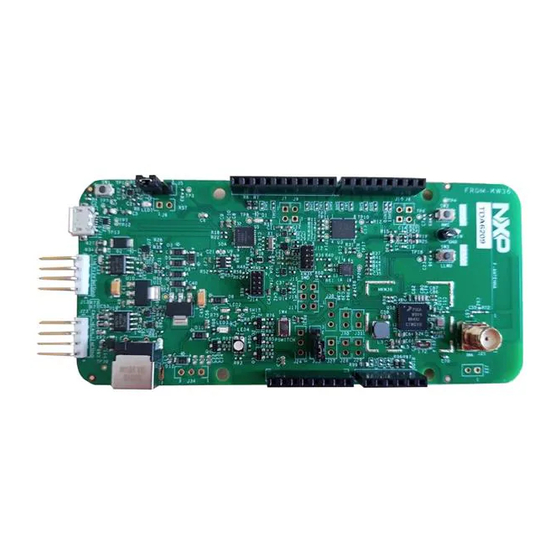
Mounted PCB 7 PCB Figure 22. PCB 8 Mounted PCB Figure 23. Mounted PCB FRDM-KW36 Minimum BoM Development Board User’s Guide, User’s Guide, Rev. 0, 09/20187 NXP Semiconductos. -
Page 21: Component Positioning
Component positioning 9 Component positioning Figure 24. Component positioning 1 FRDM-KW36 Minimum BoM Development Board User’s Guide, User’s Guide, Rev. 0, 09/20187 NXP Semiconductors... - Page 22 Component positioning Figure 25. Component positioning 2 FRDM-KW36 Minimum BoM Development Board User’s Guide, User’s Guide, Rev. 0, 09/20187 NXP Semiconductos.
-
Page 23: Bill Of Material
DC filtering 1µF Murata GRM188R61H105KAALD DC filtering YAGEO AMERICA RC0402FR-07102KL Pswitch pull-down 100KΩ (manual start only) 32MHz EXS00A-CS07637 Main clock** 32KHz EPSON ELECTRONICS FC-135 32.7680KA-A3 RTC clock FRDM-KW36 Minimum BoM Development Board User’s Guide, User’s Guide, Rev. 0, 09/20187 NXP Semiconductors... - Page 24 D2, D3, D4 Resistor R64, R120, R121 Resistor R5(buck), R10 Resistor R2 (buck) Resistor R3 (buck) Resistor R7 (buck) Resistor R67,R68,R112,R119,R183, R234 Resistor R98,R99,R134 DNP=Do Not Populate FRDM-KW36 Minimum BoM Development Board User’s Guide, User’s Guide, Rev. 0, 09/20187 NXP Semiconductos.
-
Page 25: Bypass Mode
** Refer to chapter 3.4 Clocks for alternate crystal frequencies and PNs *** Add the decoupling capacitor if the associated pin is used into the application FRDM-KW36 Minimum BoM Development Board User’s Guide, User’s Guide, Rev. 0, 09/20187 NXP Semiconductors... - Page 26 10uH Resistor 0 ohm R1 (bypass) Resistor 0 ohm R4,R6 (bypass) Resistor R64,R120,R121 Leds D2,D3,D4 Resistor 0 ohm R10, R67,R68,R112,R119,R183, R234 Resistor R98,R99,R134 DNP=Do Not Populate FRDM-KW36 Minimum BoM Development Board User’s Guide, User’s Guide, Rev. 0, 09/20187 NXP Semiconductos.
-
Page 27: References
The following references are available on KW36 Minimum BoM Board: • KW36 Minimum BoM Board Design Package 12 Revision history Rev. Date Substantive change(s) 09/2018 Initial revision. FRDM-KW36 Minimum BoM Development Board User’s Guide, User’s Guide, Rev. 0, 09/20187 NXP Semiconductors... - Page 28 Information in this document is provided solely to enable system and software implementers How to Reach Us: to use NXP products. There are no express or implied copyright licenses granted hereunder to Home Page: design or fabricate any integrated circuits based on the information in this document. NXP nxp.com reserves the right to make changes without further notice to any products herein.
Need help?
Do you have a question about the FRDM-KW36 and is the answer not in the manual?
Questions and answers