Sign In
Upload
Download
Table of Contents
Contents
Add to my manuals
Delete from my manuals
Share
URL of this page:
HTML Link:
Bookmark this page
Add
Manual will be automatically added to "My Manuals"
Print this page
×
Bookmark added
×
Added to my manuals
Manuals
Brands
Hytera Manuals
Portable Radio
PD362
Service manual
Hytera PD362 Service Manual
Pd36x series
Hide thumbs
1
2
3
4
5
6
7
8
9
10
11
12
13
14
15
16
17
18
19
20
21
22
23
24
25
26
27
28
29
30
31
32
33
34
35
36
37
38
39
40
41
42
43
44
45
46
47
48
49
50
51
52
53
54
55
56
57
58
59
60
61
62
63
64
65
66
67
68
69
70
71
72
73
74
75
76
77
78
79
80
81
82
83
84
85
86
87
88
89
90
91
92
93
94
95
96
97
98
99
100
101
102
103
104
105
106
107
108
109
110
111
112
113
114
115
116
117
118
119
120
121
122
123
124
125
126
127
128
129
130
131
132
133
134
135
136
137
138
139
140
141
page
of
141
Go
/
141
Contents
Table of Contents
Troubleshooting
Bookmarks
Table of Contents
Table of Contents
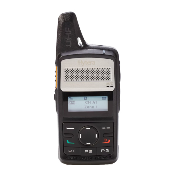
1 Product Controls
2 Disassembly and Assembly
3 Exploded View and Packaging Guide
Exploded View
Packaging Guide
4 Specifications
5 Circuit Description
Baseband
Power Supply Module
Control Module
Audio Module
RF Section
Transmitter Circuit
Receiver Circuit
6 Troubleshooting Flow Chart
Control Circuit
No Display Upon Power-On or Abnormal Display
Schematic Diagram
Parts List
Table of Contents
1 Product Controls
2 Disassembly and Assembly
3 Exploded View and Packaging Guide
Exploded View
Packaging Guide
4 Specifications
5 Circuit Description
Baseband
Power Supply Module
Control Module
Audio Module
RF Section
Transmitter Circuit
Receiver Circuit
Fgu
6 Troubleshooting Flow Chart
Control Circuit
No Display Upon Power-On or Abnormal Display
No Voice Output by Speaker
No Modulation Signal in Transmission
Receiver Circuit
Transmitter Circuit
FGU Circuit
7 Interface Definition
8 Tuning Description
Tools
Tuning Procedure
Tuning a Radio
Testing a Radio
9 PCB View
Radio General Diagram
10 Block Diagram
Radio General Diagram
RF Circuit
Baseband Circuit
Power Supply Circuit
Power Supply Circuit
FGU Circuit
FGU Circuit
Receiver Circuit
Receiver Circuit
Advertisement
Quick Links
1
Product Controls
2
Specifications
Download this manual
PORTABLE
Table of
Contents
Previous
Page
Next
Page
1
2
3
4
5
Advertisement
Chapters
Table of Contents
6
Table of Contents
74
Table of Contents
Troubleshooting
Troubleshooting Flow Chart
29
Troubleshooting Flow Chart
97
Need help?
Do you have a question about the PD362 and is the answer not in the manual?
Ask a question
Questions and answers
Related Manuals for Hytera PD362
Two-Way Radio Hytera PD365 Operating Instructions
(2 pages)
Portable Radio Hytera PD36X Owner's Manual
Digital portable radio (23 pages)
Portable Radio Hytera PD35X Owner's Manual
(27 pages)
Portable Radio Hytera PD375 Owner's Manual
(24 pages)
Portable Radio Hytera PD366 Service Manual
Pd36x series (141 pages)
Portable Radio Hytera PD368 Service Manual
Pd36x series (141 pages)
Portable Radio Hytera PD355LF Owner's Manual
(23 pages)
Portable Radio Hytera PD362i Owner's Manual
(23 pages)
Portable Radio Hytera PD-355 Owner's Manual
(27 pages)
Portable Radio Hytera PD355 Service Manual
Digital portable radio (138 pages)
Portable Radio Hytera PD78X Series System Planner Manual
Digital mobile radio (182 pages)
Portable Radio Hytera PD785 Manual
(41 pages)
Portable Radio Hytera PD98X User Manual
(19 pages)
Portable Radio Hytera PD715 Rx Owner's Manual
(14 pages)
Portable Radio Hytera PD982 Manual
(54 pages)
Portable Radio Hytera PD402i Owner's Manual
(20 pages)
This manual is also suitable for:
Pd365
Pd366
Pd368
Table of Contents
Print
Rename the bookmark
Delete bookmark?
Delete from my manuals?
Login
Sign In
OR
Sign in with Facebook
Sign in with Google
Upload manual
Upload from disk
Upload from URL


Need help?
Do you have a question about the PD362 and is the answer not in the manual?
Questions and answers