Chapters
Table of Contents

Related Manuals for IEI Technology WAFER-US15WP2


Summary of Contents for IEI Technology WAFER-US15WP2
-
Page 1: User Manual
WAFER-US15WP2 3.5" SBC IEI Technology Corp. MODEL: WAFER-US15WP2 Intel® Atom™ based 3.5" CPU Module Up to 2.0 GB DDR2, VGA, LVDS, Mini PCIe, RS-232/422/485, IDE, CompactFlash®, 6 x USB, RoHS User Manual Page i Rev. 1.02 – 9 June, 2010... - Page 2 WAFER-US15WP2 3.5" SBC Revision Date Version Changes 9 June, 2010 1.02 Modified Section 4.3 Jumper Settings. 21 May, 2010 1.01 Modified ATX power connector pin locations in Figure 3-2. 31 December, 2009 1.00 Initial release Page ii...
- Page 3 WAFER-US15WP2 3.5" SBC Copyright COPYRIGHT NOTICE The information in this document is subject to change without prior notice in order to improve reliability, design and function and does not represent a commitment on the part of the manufacturer. In no event will the manufacturer be liable for direct, indirect, special, incidental, or consequential damages arising out of the use or inability to use the product or documentation, even if advised of the possibility of such damages.
-
Page 4: Table Of Contents
WAFER-US15WP2 3.5" SBC Table of Contents 1 INTRODUCTION......................1 1.1 I ......................2 NTRODUCTION 1.2 B ........................2 ENEFITS 1.3 F ........................3 EATURES 1.4 C ......................3 ONNECTORS 1.5 D ....................... 4 IMENSIONS 1.6 D ........................ 6 1.7 T .................. - Page 5 WAFER-US15WP2 3.5" SBC 3.2.11 Keyboard/Mouse Connector................25 3.2.12 LVDS Connector (LVDS1) ................26 3.2.13 LVDS Backlight Connector (LVDS1)............. 27 3.2.14 LVDS Backlight Adjustment (LVDS1)............28 3.2.15 LVDS Connector (LVDS2) ................29 3.2.16 LVDS Backlight Connector (LVDS2)............. 30 3.2.17 Parallel Port Connector ................31 3.2.18 PCIe Mini Card Slot ..................
- Page 6 WAFER-US15WP2 3.5" SBC 5.1.3 Getting Help..................... 54 5.1.4 Unable to Reboot After Configuration Changes..........54 5.1.5 BIOS Menu Bar....................54 5.2 M ........................55 5.3 A ....................... 56 DVANCED 5.3.1 CPU Configuration..................57 5.3.2 IDE Configuration ................... 58 5.3.2.1 IDE Master, IDE Slave ................59 5.3.3 Super IO Configuration ...................
- Page 7 WAFER-US15WP2 3.5" SBC List of Figures Figure 1-1: WAFER-US15WP2 .......................2 Figure 1-2: Connectors ........................3 Figure 1-3: Dimensions without heatsink (mm) ................4 Figure 1-4: Dimensions with heatsink (mm) ................5 Figure 1-5: Data Flow Diagram......................6 Figure 3-1: Connector and Jumper Locations................14 Figure 3-2: ATX Power Connector Location ................17 Figure 3-3: ATX Standby Power Connector Location...............18...
- Page 8 WAFER-US15WP2 3.5" SBC Figure 3-26: External Interface Connectors................38 Figure 3-27: Ethernet Connector....................39 Figure 3-28: Serial Port Pinout Locations ..................40 Figure 3-29: VGA Connector .......................41 Figure 4-1: Clear CMOS Jumper Location .................46 Figure 4-2: AT/ATX Mode Selection Jumper Location..............47 Figure 4-3: LVDS Voltage Selection Jumper Location .............48 Figure 4-4: LVDS Resolution Selection Jumper Location............49...
- Page 9 WAFER-US15WP2 3.5" SBC List of Tables Table 1-1: Technical Specifications....................8 Table 2-1: Packing List.........................12 Table 2-2: Optional Items......................12 Table 3-1: Peripheral Interface Connectors ................15 Table 3-2: Rear Panel Connectors ....................16 Table 3-3: ATX Power Connector Pinouts .................17 Table 3-4: ATX Standby Power Connector Pinouts ..............18 Table 3-5: Audio Connector Pinouts ..................19...
- Page 10 WAFER-US15WP2 3.5" SBC Table 3-28: VGA Connector Pinouts...................41 Table 4-1: Jumpers ........................45 Table 4-2: Clear CMOS Jumper Settings..................46 Table 4-3: AT/ATX Mode Selection .....................47 Table 4-4: LVDS Voltage Selection .....................48 Table 4-5: LVDS Resolution Selection..................49 Table 4-6: CompactFlash® Master/Slave Selection ..............49 Table 4-7: COM3 RS-232/422/485 Selection ................50...
- Page 11 WAFER-US15WP2 3.5" SBC BIOS Menus BIOS Menu 1: Main ........................55 BIOS Menu 2: Advanced ......................56 BIOS Menu 3: CPU Configuration ....................57 BIOS Menu 4: IDE Configuration....................58 BIOS Menu 5: IDE Master and IDE Slave Configuration ............59 BIOS Menu 6: Super IO Configuration..................63 BIOS Menu 7: Hardware Health Configuration ................67...
-
Page 13: Introduction
WAFER-US15WP2 3.5" SBC Chapter Introduction Page 1... -
Page 14: Introduction
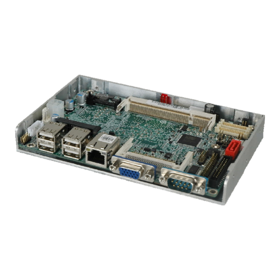
WAFER-US15WP2 3.5" SBC 1.1 Introduction Figure 1-1: WAFER-US15WP2 The WAFER-US15WP2 is a 3.5" SBC with a 1.1 GHz Intel® Atom™ Z510P or 1.6 GHz Intel® Atom™ Z530P CPU. The WAFER-US15WP2 is designed for fanless operation. The low power CPUs don't require active cooling and stay within specified heat range using the included heatsink. -
Page 15: Features
Some of the WAFER-US15WP2 motherboard features are listed below: 3.5" form factor RoHS compliant PCIe Mini card slot IDE and CompactFlash® Gigabit Ethernet 1.4 Connectors The connectors on the WAFER-US15WP2 are shown in the figure below. Figure 1-2: Connectors Page 3... -
Page 16: Dimensions
WAFER-US15WP2 3.5" SBC 1.5 Dimensions The main dimensions of the WAFER-US15WP2 are shown in the diagram below. Length: 102 mm Width: 146 mm Figure 1-3: Dimensions without heatsink (mm) Page 4... -
Page 17: Figure 1-4: Dimensions With Heatsink (Mm)
WAFER-US15WP2 3.5" SBC Figure 1-4: Dimensions with heatsink (mm) Page 5... -
Page 18: Data Flow
Figure 1-5 shows the data flow between the system chipset, the CPU and other components installed on the motherboard. Figure 1-5: Data Flow Diagram 1.7 Technical Specifications WAFER-US15WP2 technical specifications are listed in Table 1-1. Specification WAFER-US15WP2 Form Factor 3.5"... - Page 19 WAFER-US15WP2 3.5" SBC Specification WAFER-US15WP2 Z510P: 400 MHz Front Side Bus (FSB) Z530P: 533 MHz System Chipset Intel® US15WP Memory 200-pin DDR2 SO-DIMM up to 2.0 GB Z510P: only 400/533/667 MHz (800 MHz not supported) Z530P: only 533/667/800 MHz (400 MHz not supported)
-
Page 20: Table 1-1: Technical Specifications
WAFER-US15WP2 3.5" SBC Specification WAFER-US15WP2 Physical Specifications Dimensions 102 mm x 146 mm Weight GW/NW 700 g/350 g Table 1-1: Technical Specifications Page 8... -
Page 21: Packing List
WAFER-US15WP2 3.5" SBC Chapter Packing List Page 9... -
Page 22: Anti-Static Precautions
Only handle the edges of the PCB:- Don't touch the surface of the motherboard. Hold the motherboard by the edges when handling. 2.2 Unpacking Precautions When the WAFER-US15WP2 is unpacked, please do the following: Follow the antistatic guidelines above. Make sure the packing box is facing upwards when opening. -
Page 23: Packing List
If any of the components listed in the checklist below are missing, do not proceed with the installation. Contact the IEI reseller or vendor the WAFER-US15WP2 was purchased from or contact an IEI sales representative directly by sending an email to sales@iei.com.tw. -
Page 24: Optional Items
WAFER-US15WP2 3.5" SBC Quantity Item and Part Number Image Utility CD Quick installation guide Table 2-1: Packing List 2.4 Optional Items These optional items are available. Item and Part Number Image Dual USB cable (wo bracket) (P/N: 32000-070301-RS) LPT cable (wo bracket) -
Page 25: Connector Pinouts
WAFER-US15WP2 3.5" SBC Chapter Connector Pinouts Page 13... -
Page 26: Peripheral Interface Connectors
WAFER-US15WP2 3.5" SBC 3.1 Peripheral Interface Connectors Section 3.1.2 shows peripheral interface connector locations. Section 3.1.2 lists all the peripheral interface connectors seen in Section 3.1.2. 3.1.1 Layout The figure below shows the on-board peripheral connectors, rear panel peripheral connectors and on-board jumpers. -
Page 27: Peripheral Interface Connectors
WAFER-US15WP2 3.5" SBC 3.1.2 Peripheral Interface Connectors The table below shows a list of the peripheral interface connectors on the WAFER-US15WP2. Detailed descriptions of these connectors can be found below. Connector Type Label ATX power connector Molex PWR1 ATX standby power connector... -
Page 28: External Interface Panel Connectors
WAFER-US15WP2 3.5" SBC 3.1.3 External Interface Panel Connectors The table below lists the rear panel connectors on the WAFER-US15WP2. Detailed descriptions of these connectors can be found in a later section. Connector Type Label USB connectors Dual-USB USB1, USB2 LAN connector... -
Page 29: Atx Standby Power Connector
WAFER-US15WP2 3.5" SBC Figure 3-2: ATX Power Connector Location Description Description Ground Ground EXT_VIN EXT_VIN Table 3-3: ATX Power Connector Pinouts 3.2.2 ATX Standby Power Connector CN Label: PSON1 CN Type: 3-pin wafer CN Location: See Figure 3-3 See Table 3-4 CN Pinouts: Provides standby power to the system when the system is turned off. -
Page 30: Audio Connector
WAFER-US15WP2 3.5" SBC Figure 3-3: ATX Standby Power Connector Location Description 5VSB PS_ON- Ground Table 3-4: ATX Standby Power Connector Pinouts 3.2.3 Audio Connector CN Label: AUDIO1 CN Type: 10-pin header CN Location: See Figure 3-4 CN Pinouts: See Table 3-5 This header provides a line output and microphone input. -
Page 31: Battery Connector
WAFER-US15WP2 3.5" SBC Figure 3-4: Audio Connector Locations Description Description Speaker_R Line_In_R Speaker_L Line_In_L MIC_R MIC_L Table 3-5: Audio Connector Pinouts 3.2.4 Battery Connector CN Label: CN Type: 2-pin wafer (1x2) See Figure 3-5 CN Location: See Table 3-6 CN Pinouts: This is connected to the system battery. -
Page 32: Compactflash® Slot
WAFER-US15WP2 3.5" SBC Figure 3-5: Battery Connector Location Description Battery+ Ground Table 3-6: Battery Connector Pinouts 3.2.5 CompactFlash® Slot CN Label: CN Type: CompactFlash® card slot CN Location: See Figure 3-6 NOTE: 1. Only CompactFlash® Type I cards are supported 2. -
Page 33: Digital I/O Connector
WAFER-US15WP2 3.5" SBC Figure 3-6: CompactFlash® Slot Location 3.2.6 Digital I/O Connector CN Label: DIO1 10-pin header CN Type: CN Location: See Figure 3-7 CN Pinouts: See Table 3-7 The digital I/O connector provides programmable input and output for external devices. -
Page 34: Dimm Connector
WAFER-US15WP2 3.5" SBC Description Description Output 3 Output 2 Output 1 Output 0 Input 3 Input 2 Input 1 Input 0 Table 3-7: Digital I/O Connector Pinouts 3.2.7 DIMM Connector CN Label: DIMM1 CN Type: DIMM connector CN Location: See Figure 3-8... -
Page 35: Fan Connector
WAFER-US15WP2 3.5" SBC Figure 3-8: DVI Connector Location 3.2.8 Fan Connector CN Label: FAN1 3-pin header CN Type: CN Location: See Figure 3-9 CN Pinouts: See Table 3-8 Connects to a system cooling fan. Figure 3-9: Fan Connector Location Page 23... -
Page 36: Front Panel Connector
WAFER-US15WP2 3.5" SBC Description Sensor +12 V Ground Table 3-8: Fan Connector Pinouts 3.2.9 Front Panel Connector CN Label: F_PANEL1 CN Type: 10-pin header (2x5) CN Location: See Figure 3-10 CN Pinouts: See Table 3-9 The front panel connector connects to external switches and indicators to monitor and control the motherboard. -
Page 37: Infrared Interface Connector
WAFER-US15WP2 3.5" SBC Description Description Power button+ Power button- Table 3-9: Front Panel Connector Pinouts 3.2.10 Infrared Interface Connector CN Label: 5-pin header (1x5) CN Type: CN Location: See Figure 3-11 CN Pinouts: See Table 3-10 The infrared connector attaches to an infrared receiver for use with remote controls. -
Page 38: Lvds Connector (Lvds1)
WAFER-US15WP2 3.5" SBC CN Location: See Figure 3-12 CN Pinouts: See Table 3-11 Connects to a PS/2 keyboard or mouse. Figure 3-12: Keyboard/Mouse Connector Location Description Description +5 V MS_DATA MS_CLOCK KB_DATA KB_CLOCK Table 3-11: Keyboard/Mouse Connector Pinouts 3.2.12 LVDS Connector (LVDS1) -
Page 39: Lvds Backlight Connector (Lvds1)
WAFER-US15WP2 3.5" SBC The LVDS connector is for an LCD panel connected to the board. Figure 3-13: LVDS1 Connector Location Description Description GROUND GROUND 1st LVDS Data0+ 1st LVDS Data0- 1st LVDS Data1+ 1st LVDS Data1- 1st LVDS Data2+ 1st LVDS Data2-... -
Page 40: Lvds Backlight Adjustment (Lvds1)
WAFER-US15WP2 3.5" SBC CN Location: See Figure 3-14 CN Pinouts: See Table 3-13 Provides power for the LCD backlight. Figure 3-14: Backlight Inverter Connector Description BLADJ# 12 V BLEN# Table 3-13: Backlight Inverter Connector 3.2.14 LVDS Backlight Adjustment (LVDS1) CN Label:... -
Page 41: Lvds Connector (Lvds2)
WAFER-US15WP2 3.5" SBC Figure 3-15: LPC Connector Location Description Description LED-BL LED-AM menu/enter DOWN auto/exit POWER Table 3-14: LPC Connector Pinouts 3.2.15 LVDS Connector (LVDS2) CN Label: LVDS2 CN Type: 30-pin crimp (2x15) CN Location: See Figure 3-13 CN Pinouts: See Table 3-12 The LVDS connector is for an LCD panel connected to the board. -
Page 42: Lvds Backlight Connector (Lvds2)
WAFER-US15WP2 3.5" SBC Figure 3-16: LVDS2 Connector Location Description Description GROUND GROUND Data0+ Data0- Data1+ Data1- Data2+ Data2- Clock+ Clock- Data3+ Data3- GROUND GROUND GROUND GROUND Table 3-15: LVDS2 Connector Pinouts 3.2.16 LVDS Backlight Connector (LVDS2) CN Label: INV2 5-pin box header... -
Page 43: Parallel Port Connector
WAFER-US15WP2 3.5" SBC Provides power for the LCD backlight. Figure 3-17: Backlight Inverter Connector Description BRIGHTNESS 12 V ENABKL Table 3-16: Backlight Inverter Connector 3.2.17 Parallel Port Connector CN Label: LPT1 26-pin box header CN Type: CN Location: See Figure 3-18... -
Page 44: Pcie Mini Card Slot
WAFER-US15WP2 3.5" SBC Figure 3-18: Parallel Port Connector Location Description Description -STB# -AFD PTD0 -ERR PTD1 -INIT PTD2 -SLIN PTD3 GROUND PTD4 GROUND PTD5 GROUND PTD6 GROUND PTD7 GROUND -ACK GROUND BUSY GROUND GROUND SLCT Table 3-17: Parallel Port Connector Pinouts 3.2.18 PCIe Mini Card Slot... -
Page 45: Sata Drive Connectors
WAFER-US15WP2 3.5" SBC Figure 3-19: PCIe Mini Card Slot Location 3.2.19 SATA Drive Connectors CN Label: SATA1 CN Type: 7-pin SATA drive connectors CN Location: See Figure 3-20 See Table 3-18 CN Pinouts: The SATA connectors connect to SATA hard drives or optical drives. -
Page 46: Sata Power Connectors
WAFER-US15WP2 3.5" SBC Description Table 3-18: SATA Drive Connector Pinouts 3.2.20 SATA Power Connectors CN Label: PWR2 CN Type: 2-pin wafer CN Location: See Figure 3-21 CN Pinouts: See Table 3-19 Use the SATA Power Connector to connect to SATA device power connections. -
Page 47: Serial Port Connector
WAFER-US15WP2 3.5" SBC CN Location: See Figure 3-22 CN Pinouts: See Table 3-20 This connector provides RS-232 communications. Figure 3-22: Serial Port Connector Location Description Description Data Carrier Direct (DCD) Data Set Ready (DSR) Receive Data (RXD) Request To Send (RTS) -
Page 48: Serial Port Connector
WAFER-US15WP2 3.5" SBC Figure 3-23: Serial Port Connector Location Description Description NDCD2 NDSR2 NRX2 NRTS2 NTX2 NCTS2 NDTR2 NRI2 TX2+ (RS-422) TX2- (RS-422) D+ (RS-485) D- (RS-485) RX2+ (RS-422) RX2- (RS-422) Table 3-21: Serial Port Connector Pinouts 3.2.23 Serial Port Connector... -
Page 49: Usb Connector
WAFER-US15WP2 3.5" SBC Figure 3-24: Serial Port Connector Location Description Description Data Carrier Direct (DCD) Data Set Ready (DSR) Receive Data (RXD) Request To Send (RTS) Transmit Data (TXD) Clear To Send (CTS) Data Terminal Ready (DTR) Ring Indicator (RI) -
Page 50: External Interface Connectors
DATA5+ DATA4+ DATA5- Table 3-23: USB Port Connector Pinouts 3.3 External Interface Connectors Figure 3-26 shows the WAFER-US15WP2 motherboard external interface connectors. The WAFER-US15WP2 on-board external interface connectors are shown in Figure 3-26. Figure 3-26: External Interface Connectors Page 38... -
Page 51: Ethernet Connector
WAFER-US15WP2 3.5" SBC 3.3.1 Ethernet Connector CN Label: LAN1 RJ-45 CN Type: See Figure 3-26 CN Location: CN Pinouts: See Table 3-24 A 10/100/1000 Mb/s connection can be made to a Local Area Network. Description Description MDIA0+ MDIA2+ MDIA0- MDIA2-... -
Page 52: Usb Ports
WAFER-US15WP2 3.5" SBC CN Location: See Figure 3-26 CN Pinouts: See Table 3-26 and Figure 3-28 The RS-232 serial connector provides serial connection in the RS-232 mode. Description Description Table 3-26: Serial Port Pinouts Figure 3-28: Serial Port Pinout Locations 3.3.3 USB Ports... -
Page 53: Vga Connector
WAFER-US15WP2 3.5" SBC Description Ground Data2- Data2+ Ground Table 3-27: USB Connector Pinouts 3.3.4 VGA Connector CN Label: VGA1 CN Type: D-sub 15-pin female connector CN Location: See Figure 3-26 CN Pinouts: See Figure 3-29 an Table 3-28 The standard 15-pin female VGA connector connects to a CRT or LCD monitor. -
Page 54: Installation
WAFER-US15WP2 3.5" SBC Chapter Installation Page 42... -
Page 55: Anti-Static Precautions
Electrostatic discharge (ESD) can cause serious damage to electronic components, including the WAFER-US15WP2. Dry climates are especially susceptible to ESD. It is therefore critical to strictly adhere to the following anti-static precautions whenever the WAFER-US15WP2, or any other electrical component, is handled. - Page 56 Make sure the product is disconnected from all power supplies and that no electricity is being fed into the system. Before and during the installation of the WAFER-US15WP2 DO NOT: DO NOT remove any of the stickers on the PCB board. These stickers are required for warranty validation.
-
Page 57: Jumper Settings
OPEN a jumper means removing the plastic clip from a jumper. Before the WAFER-US15WP2 is installed in the system, the jumpers must be set in accordance with the desired configuration. The jumpers on the WAFER-US15WP2 are listed in Table 4-1. -
Page 58: Figure 4-1: Clear Cmos Jumper Location
Jumper Location: See Figure 4-1 If the WAFER-US15WP2 fails to boot due to improper BIOS settings, the clear CMOS jumper clears the CMOS data and resets the system BIOS information. To do this, use the jumper cap to close pins 2 and 3 for a few seconds then reinstall the jumper clip back to pins 1 and 2. -
Page 59: At/Atx Mode Selection
Jumper Location: See Figure 4-2 Set both of the jumpers select AT or ATX power mode for the WAFER-US15WP2. AT power mode limits the system to on/off. ATX allows the system to use various power saving states and enter a standby state, so the system can be turned on remotely over a network. -
Page 60: Lvds Resolution Selection (For Lvds1)
WAFER-US15WP2 3.5" SBC Selects the voltage of the LVDS connector. The J_VLVDS1 jumper is for LVDS1 connector; the J_VLVDS2 jumper is for LVDS2 connector Description +3.3 V +5 V (Default) +12 V Table 4-4: LVDS Voltage Selection Figure 4-3: LVDS Voltage Selection Jumper Location 4.3.4 LVDS Resolution Selection (for LVDS1) -
Page 61: Compactflash® Master/Slave Selection
WAFER-US15WP2 3.5" SBC Description Short 1-2, 3-4 1280 x 1024 (Default) Short 5-6 1366 x 768 Short 1-2, 5-6 1920 x 1080 Table 4-5: LVDS Resolution Selection Figure 4-4: LVDS Resolution Selection Jumper Location 4.3.5 CompactFlash® Master/Slave Selection Jumper Label:... -
Page 62: Com3 Rs-232/422/485 Selection
WAFER-US15WP2 3.5" SBC Figure 4-5: CompactFlash® Master/Slave Selection Jumper Location 4.3.6 COM3 RS-232/422/485 Selection Jumper Label: Jumper Type: 3-pin header Jumper Settings: See Table 4-7 Jumper Location: See Figure 4-6 Selects the communication method of COM3 serial port. Description RS-232 (Default) - Page 63 WAFER-US15WP2 3.5" SBC Page 51...
-
Page 64: Bios
WAFER-US15WP2 3.5" SBC Chapter BIOS Page 52... -
Page 65: Introduction
WAFER-US15WP2 3.5" SBC 5.1 Introduction The BIOS is programmed onto the BIOS chip. The BIOS setup program allows changes to certain system settings. This chapter outlines the options that can be changed. 5.1.1 Starting Setup The AMI BIOS is activated when the computer is turned on. The setup program can be activated in one of two ways. -
Page 66: Getting Help
WAFER-US15WP2 3.5" SBC Function F2 /F3 key Change color from total 16 colors. F2 to select color forward. F10 key Save all the CMOS changes, only for Main Menu Table 5-1: BIOS Navigation Keys 5.1.3 Getting Help When F1 is pressed a small help window describing the appropriate keys to use and the possible selections for the highlighted item appears. -
Page 67: Main
WAFER-US15WP2 3.5" SBC 5.2 Main The Main BIOS menu (BIOS Menu 1) appears when the BIOS Setup program is entered. The Main menu gives an overview of the basic system information. BIOS SETUP UTILITY Main Advanced PCIPNP Boot Security Chipset... -
Page 68: Advanced
WAFER-US15WP2 3.5" SBC Size: Lists memory size The System Overview field also has two user configurable fields: System Time [xx:xx:xx] Use the System Time option to set the system time. Manually enter the hours, minutes and seconds. System Date [xx/xx/xx] Use the System Date option to set the system date. -
Page 69: Cpu Configuration
WAFER-US15WP2 3.5" SBC 5.3.1 CPU Configuration Use the CPU Configuration menu (BIOS Menu 3) to view detailed CPU specifications and configure the CPU. BIOS SETUP UTILITY Main Advanced PCIPNP Boot Security Chipset Exit Configure Advanced CPU Settings Module Version:3F.14 ⎯⎯⎯⎯⎯⎯⎯⎯⎯⎯⎯⎯⎯⎯⎯⎯⎯⎯⎯⎯⎯⎯⎯⎯⎯⎯⎯⎯⎯⎯⎯... -
Page 70: Ide Configuration
WAFER-US15WP2 3.5" SBC 5.3.2 IDE Configuration Use the IDE Configuration menu (BIOS Menu 4) to change and/or set the configuration of the IDE devices installed in the system. BIOS SETUP UTILITY Main Advanced PCIPNP Boot Security Chipset Exit IDE Configuration Options ⎯⎯⎯⎯⎯⎯⎯⎯⎯⎯⎯⎯⎯⎯⎯⎯⎯⎯⎯⎯⎯⎯⎯⎯⎯⎯⎯⎯⎯⎯⎯... -
Page 71: Ide Master, Ide Slave
WAFER-US15WP2 3.5" SBC 5.3.2.1 IDE Master, IDE Slave Use the IDE Master and IDE Slave configuration menu to view both primary and secondary IDE device details and configure the IDE devices connected to the system. BIOS SETUP UTILITY Main Advanced... -
Page 72: Type [Auto]
WAFER-US15WP2 3.5" SBC Async DMA: Indicates the highest Asynchronous DMA Mode that is supported. Ultra DMA: Indicates the highest Synchronous DMA Mode that is supported. S.M.A.R.T.: Indicates whether or not the Self-Monitoring Analysis and Reporting Technology protocol is supported. 32Bit Data Transfer: Enables 32-bit data transfer. -
Page 73: Block (Multi Sector Transfer) [Auto]
WAFER-US15WP2 3.5" SBC Auto BIOS auto detects the LBA mode control on the specified EFAULT channel. Block (Multi Sector Transfer) [Auto] Use the Block (Multi Sector Transfer) to disable or enable BIOS to auto detect if the device supports multi-sector transfers. -
Page 74: Dma Mode [Auto]
WAFER-US15WP2 3.5" SBC DMA Mode [Auto] Use the DMA Mode BIOS selection to adjust the DMA mode options. BIOS auto detects the DMA mode. Use this value if the IDE Auto EFAULT disk drive support cannot be determined. Single Word DMA mode 0, max transfer rate: 2.1 MB/s... -
Page 75: Super Io Configuration
WAFER-US15WP2 3.5" SBC 32Bit Data Transfer [Enabled] Use the 32Bit Data Transfer BIOS option to enables or disable 32-bit data transfers. Prevents the BIOS from using 32-bit data transfers. Disabled Enabled Allows BIOS to use 32-bit data transfers on supported EFAULT hard disk drives. -
Page 76: Serial Port1 Irq [Irq3]
WAFER-US15WP2 3.5" SBC Serial Port1 IRQ [IRQ3] The Serial Port1 IRQ option sets the interrupt for serial port1. IRQ3 EFAULT IRQ4 Serial Port2 Address [2F8] The Serial Port2 Address option sets the base address for serial port2. Disabled EFAULT Serial Port2 IRQ [IRQ4] The Serial Port2 IRQ option sets the interrupt for serial port2. -
Page 77: Serial Port4 Address [2E8]
WAFER-US15WP2 3.5" SBC Serial Port4 Address [2E8] The Serial Port4 Address option sets the base address for serial port4. Disabled EFAULT Serial Port4 IRQ [IRQ4] The Serial Port4 IRQ option sets the interrupt for serial port4. IRQ3 IRQ4 EFAULT IR Function Address [2E0] The IR Function Address option sets the base address for the IR port. -
Page 78: Parallel Port Mode [Normal]
WAFER-US15WP2 3.5" SBC EFAULT Parallel Port Mode [Normal] The Parallel Port Mode option to select the mode the parallel port operates in. Normal The normal parallel port mode is the standard mode EFAULT for parallel port operation. Parallel port outputs are 8-bits long. Inputs are... -
Page 79: Hardware Health Configuration
WAFER-US15WP2 3.5" SBC 5.3.4 Hardware Health Configuration The Hardware Health Configuration menu (BIOS Menu 7) shows the operating temperature, fan speeds and system voltages. BIOS SETUP UTILITY Main Advanced PCIPNP Boot Security Chipset Exit Hardware Health Event Monitoring Fan configuration ⎯⎯⎯⎯⎯⎯⎯⎯⎯⎯⎯⎯⎯⎯⎯⎯⎯⎯⎯⎯⎯⎯⎯⎯⎯⎯⎯⎯⎯⎯⎯... -
Page 80: Cpu Temperature Limit Of Off [000]
WAFER-US15WP2 3.5" SBC CPU Temperature Limit of OFF [000] WARNING: CPU failure can result if this value is set too high because the fan will turn off before the CPU has been cooled to the normal temperature range The fan will turn off if the temperature falls below this value. -
Page 81: Remote Access Configuration
WAFER-US15WP2 3.5" SBC 0.125 PWM 0.25 PWM 0.5 PWM 1 PWM 2 PWM 4 PWM 8 PWM 15 PWM 5.3.5 Remote Access Configuration Use the Remote Access Configuration menu (BIOS Menu 8) to configure remote access parameters. The Remote Access Configuration is an AMIBIOS feature and allows a remote host running a terminal program to display and configure the BIOS settings. -
Page 82: Serial Port Number [Com1]
WAFER-US15WP2 3.5" SBC Enabled Remote access configuration options shown below appear: Serial Port Number Serial Port Mode Redirection after BIOS POST Terminal Type These configuration options are discussed below. Serial Port Number [COM1] Use the Serial Port Number option allows to select the serial port used for remote access. -
Page 83: Redirection After Bios Post [Always]
WAFER-US15WP2 3.5" SBC NOTE: Identical baud rate setting musts be set on the host (a management computer running a terminal software) and the slave Redirection After BIOS POST [Always] Use the Redirection After BIOS POST option to specify when console redirection should occur. -
Page 84: Usb Configuration
WAFER-US15WP2 3.5" SBC 5.3.6 USB Configuration Use the USB Configuration menu (BIOS Menu 9) to read USB configuration information and configure the USB settings. BIOS SETUP UTILITY Main Advanced PCIPNP Boot Security Chipset Exit USB Configuration Options ⎯⎯⎯⎯⎯⎯⎯⎯⎯⎯⎯⎯⎯⎯⎯⎯⎯⎯⎯⎯⎯⎯⎯⎯⎯⎯⎯⎯⎯⎯⎯ Disabled Module Version – 2.24.3-13.4... -
Page 85: Legacy Usb Support [Enabled]
WAFER-US15WP2 3.5" SBC Legacy USB Support [Enabled] Use the Legacy USB Support BIOS option to enable USB mouse and USB keyboard support. Normally if this option is not enabled, any attached USB mouse or USB keyboard does not become available until a USB compatible operating system is fully booted with all USB drivers loaded. -
Page 86: Usb Mass Storage Device Configuration
WAFER-US15WP2 3.5" SBC 5.3.6.1 USB Mass Storage Device Configuration Use the USB Mass Storage Device Configuration menu (BIOS Menu 10) to configure USB mass storage class devices. BIOS SETUP UTILITY Main Advanced PCIPNP Boot Security Chipset Exit USB Mass Storage Device Configuration ⎯⎯⎯⎯⎯⎯⎯⎯⎯⎯⎯⎯⎯⎯⎯⎯⎯⎯⎯⎯⎯⎯⎯⎯⎯⎯⎯⎯⎯⎯⎯... -
Page 87: Emulation Type [Auto]
WAFER-US15WP2 3.5" SBC Emulation Type [Auto] Use the Emulation Type BIOS option to specify the type of emulation BIOS has to provide for the USB device. Auto BIOS auto-detects the current USB. EFAULT The USB device will be emulated as a floppy drive. -
Page 88: Pci/Pnp
WAFER-US15WP2 3.5" SBC 5.4 PCI/PnP Use the PCI/PnP menu (BIOS Menu 11) to configure advanced PCI and PnP settings. BIOS SETUP UTILITY Main Advanced PCIPNP Boot Security Chipset Exit Advanced PCI/PnP Settings Available: Specified ⎯⎯⎯⎯⎯⎯⎯⎯⎯⎯⎯⎯⎯⎯⎯⎯⎯⎯⎯⎯⎯⎯⎯⎯⎯⎯⎯⎯⎯⎯⎯ IRQ is available to be... -
Page 89: Boot
WAFER-US15WP2 3.5" SBC 16 KB reserved for legacy ISA devices 32 KB reserved for legacy ISA devices 64 KB reserved for legacy ISA devices 5.5 Boot Use the Boot menu (BIOS Menu 12) to configure system boot options. BIOS SETUP UTILITY... -
Page 90: Boot Settings Configuration
WAFER-US15WP2 3.5" SBC 5.5.1 Boot Settings Configuration Use the Boot Settings Configuration menu (BIOS Menu 13) to configure advanced system boot options. BIOS SETUP UTILITY Main Advanced PCIPNP Boot Security Chipset Exit Boot Settings Configuration Allows BIOS to skip ⎯⎯⎯⎯⎯⎯⎯⎯⎯⎯⎯⎯⎯⎯⎯⎯⎯⎯⎯⎯⎯⎯⎯⎯⎯⎯⎯⎯⎯⎯⎯... -
Page 91: Addon Rom Display Mode [Force Bios]
WAFER-US15WP2 3.5" SBC AddOn ROM Display Mode [Force BIOS] Use the AddOn ROM Display Mode option to allow add-on ROM (read-only memory) messages to be displayed. Force BIOS The system forces third party BIOS to display EFAULT during system boot. -
Page 92: Boot Device Priority
WAFER-US15WP2 3.5" SBC 5.5.2 Boot Device Priority Use the Boot Device Priority menu (BIOS Menu 14) to specify the boot sequence from the available devices. The drive sequence also depends on the boot sequence in the individual device section. BIOS SETUP UTILITY... -
Page 93: Hard Disk Drives
WAFER-US15WP2 3.5" SBC 5.5.3 Hard Disk Drives Use the Hard Disk Drives menu to specify the boot sequence of the available HDDs. Only installed hard drives are shown. BIOS SETUP UTILITY Main Advanced PCIPNP Boot Security Chipset Exit Hard Disk Drives Specifies the boot ⎯⎯⎯⎯⎯⎯⎯⎯⎯⎯⎯⎯⎯⎯⎯⎯⎯⎯⎯⎯⎯⎯⎯⎯⎯⎯⎯⎯⎯⎯⎯... -
Page 94: Cd/Dvd Drives
WAFER-US15WP2 3.5" SBC 5.5.5 CD/DVD Drives Use the CD/DVD Drives menu to specify the boot sequence of the available CD/DVD drives. Only connected drives are shown. BIOS SETUP UTILITY Main Advanced PCIPNP Boot Security Chipset Exit Hard Disk Drives Specifies the boot ⎯⎯⎯⎯⎯⎯⎯⎯⎯⎯⎯⎯⎯⎯⎯⎯⎯⎯⎯⎯⎯⎯⎯⎯⎯⎯⎯⎯⎯⎯⎯... -
Page 95: Chipset
WAFER-US15WP2 3.5" SBC Change Supervisor Password Use the Change Supervisor Password to set or change a supervisor password. The default for this option is Not Installed. If a supervisor password must be installed, select this field and enter the password. After the password has been added, Install appears next to Change Supervisor Password. -
Page 96: Northbridge Configuration
WAFER-US15WP2 3.5" SBC 5.7.1 Northbridge Configuration Use the Northbridge Chipset Configuration menu (BIOS Menu 20) to configure the Northbridge chipset. BIOS SETUP UTILITY Main Advanced PCIPNP Boot Security Chipset Exit Northbridge Configuration Select the amount of ⎯⎯⎯⎯⎯⎯⎯⎯⎯⎯⎯⎯⎯⎯⎯⎯⎯⎯⎯⎯⎯⎯⎯⎯⎯⎯⎯⎯⎯⎯⎯ system memory used by... -
Page 97: Lvds2 Panel Type [1024 X 768]
WAFER-US15WP2 3.5" SBC LVDS2 Panel Type [1024 x 768] This option specifies the resolution of the flat panel display. 640x480 (generic) 800x600 (generic) 1024x768 (generic) EFAULT 640x480 (NEC 8.4") 800x480 (NEC 9") 1024x600 (TMD 5.61") 1024x600 (Samsung 4.8") 1024x768 (Samsung 15") 1280x768 (Sharp 7.2") -
Page 98: Southbridge Configuration
WAFER-US15WP2 3.5" SBC 5.7.2 Southbridge Configuration The Southbridge Configuration menu (BIOS Menu 21) the Southbridge chipset to be configured. BIOS SETUP UTILITY Main Advanced PCIPNP Boot Security Chipset Exit Southbridge Chipset Configuration Options ⎯⎯⎯⎯⎯⎯⎯⎯⎯⎯⎯⎯⎯⎯⎯⎯⎯⎯⎯⎯⎯⎯⎯⎯⎯⎯⎯⎯⎯⎯⎯ Auto Audio Controller Codec [Auto] Azalia... -
Page 99: Exit
WAFER-US15WP2 3.5" SBC 5.8 Exit Use the Exit menu (BIOS Menu 22) to load default BIOS values, optimal failsafe values and to save configuration changes. BIOS SETUP UTILITY Main Advanced PCIPNP Boot Security Chipset Exit Exit Options Exit system setup after ⎯⎯⎯⎯⎯⎯⎯⎯⎯⎯⎯⎯⎯⎯⎯⎯⎯⎯⎯⎯⎯⎯⎯⎯⎯⎯⎯⎯⎯⎯⎯... -
Page 100: Load Failsafe Defaults
WAFER-US15WP2 3.5" SBC Load Failsafe Defaults Use the Load Failsafe Defaults option to load failsafe default values for each of the parameters on the Setup menus. F8 key can be used for this operation. Page 88... -
Page 101: Abios Options
WAFER-US15WP2 3.5" SBC Appendix BIOS Options Page 89... - Page 102 WAFER-US15WP2 3.5" SBC Below is a list of BIOS configuration options in the BIOS chapter. System Overview .........................55 System Time [xx:xx:xx] .......................56 System Date [xx/xx/xx] ......................56 Onboard PCI IDE Controller [Primary]................58 IDE Master and IDE Slave....................58 ...
- Page 103 WAFER-US15WP2 3.5" SBC Base Address, IRQ [3F8h,4]....................70 Serial Port Mode [115200 8,n,1]..................70 Redirection After BIOS POST [Always] ................71 Terminal Type [ANSI]......................71 USB Function [Enabled]......................72 USB 2.0 Controller [Enabled]....................72 Legacy USB Support [Enabled]..................73 ...
-
Page 104: B Terminology
WAFER-US15WP2 3.5" SBC Appendix Terminology Page 92... - Page 105 WAFER-US15WP2 3.5" SBC AC ’97 Audio Codec 97 (AC’97) refers to a codec standard developed by Intel® in 1997. ACPI Advanced Configuration and Power Interface (ACPI) is an OS-directed configuration, power management, and thermal management interface. AHCI Advanced Host Controller Interface (AHCI) is a SATA Host controller register-level interface.
- Page 106 WAFER-US15WP2 3.5" SBC Direct Memory Access (DMA) enables some peripheral devices to bypass the system processor and communicate directly with the system memory. DIMM Dual Inline Memory Modules are a type of RAM that offer a 64-bit data bus and have separate electrical contacts on each side of the module.
- Page 107 WAFER-US15WP2 3.5" SBC Liquid crystal display (LCD) is a flat, low-power display device that consists of two polarizing plates with a liquid crystal panel in between. LVDS Low-voltage differential signaling (LVDS) is a dual-wire, high-speed differential electrical signaling system commonly used to connect LCD displays to a computer.
-
Page 108: Clvds1 Panel Support
WAFER-US15WP2 3.5" SBC Appendix LVDS1 Panel Support Page 96... -
Page 109: Table C-1: Lvds1 Panel Support
WAFER-US15WP2 3.5" SBC The following panels have been tested and are supported by LVDS1 on the WAFER-US15WP2. Other, untested, panels may or may not work. Panel Name Part Number Max Resolution Panel Size AUO G121SN01 V3 23000-000154-RS 800x600 12.1" AUO G150XG01 V1... -
Page 110: D Hazardous Materials Disclosure
WAFER-US15WP2 3.5" SBC Appendix Hazardous Materials Disclosure Page 98... -
Page 111: Hazardous Materials Disclosure Table For Ipb Products Certified As Rohs Compliant Under 2002/95/Ec Without Mercury
WAFER-US15WP2 3.5" SBC D.1 Hazardous Materials Disclosure Table for IPB Products Certified as RoHS Compliant Under 2002/95/EC Without Mercury The details provided in this appendix are to ensure that the product is compliant with the Peoples Republic of China (China) RoHS standards. The table below acknowledges the presences of small quantities of certain materials in the product, and is applicable to China RoHS only. - Page 112 WAFER-US15WP2 3.5" SBC Part Name Toxic or Hazardous Substances and Elements Lead Mercury Cadmium Hexavalent Polybrominated Polybrominated Biphenyls Diphenyl (Pb) (Hg) (Cd) Chromium (CR(VI)) (PBB) Ethers (PBDE) Housing Display Printed Circuit Board Metal Fasteners Cable Assembly Fan Assembly Power Supply...
- Page 113 WAFER-US15WP2 3.5" SBC 此附件旨在确保本产品符合中国 RoHS 标准。以下表格标示此产品中某有毒物质的含量符 合中国 RoHS 标准规定的限量要求。 本产品上会附有”环境友好使用期限”的标签,此期限是估算这些物质”不会有泄漏或突变”的 年限。本产品可能包含有较短的环境友好使用期限的可替换元件,像是电池或灯管,这些元 件将会单独标示出来。 部件名称 有毒有害物质或元素 铅 汞 镉 六价铬 多溴联苯 多溴二苯 醚 (Pb) (Hg) (Cd) (CR(VI)) (PBB) (PBDE) 壳体 显示 印刷电路板 金属螺帽 电缆组装 风扇组装 电力供应组装 电池 O: 表示该有毒有害物质在该部件所有物质材料中的含量均在 SJ/T11363-2006 标准规定的限量要求以下。 X: 表示该有毒有害物质至少在该部件的某一均质材料中的含量超出 SJ/T11363-2006 标准规定的限量要求。...
Need help?
Do you have a question about the WAFER-US15WP2 and is the answer not in the manual?
Questions and answers