Advertisement
Table of Contents
- 1 Table of Contents
- 2 Technical Specifications
- 3 Factory/Service Mode
- 4 How to Disassemble
- 5 Lcd Contrast Adjustment
- 6 Dsp(Qd01) Firmware Update Procedure
- 7 Main Microprocessor (Qu01) Update Procedure
- 8 Wiring Diagram
- 9 Block Diagram
- 10 Schematic Diagram
- 11 Parts Location
- 12 Microprocessor and IC Data
- 13 Exploded View and Parts List
- 14 Electrical Parts List
- Download this manual
Service
Manual
+
SECTION
1. TECHNICAL SPECIFICATIONS ................................................................................................... 1
2. FACTORY/SERVICE MODE ......................................................................................................... 2
3. LCD CONTRAST ADJUSTMENT ................................................................................................. 3
4. HOW TO DISASSEMBLE.............................................................................................................. 3
5. DSP(QD01) FIRMWARE UPDATE PROCEDURE........................................................................ 7
6. MAIN MICROPROCESSOR (QU01) UPDATE PROCEDURE...................................................... 9
7. WIRING DIAGRAM ..................................................................................................................... 15
8. BLOCK DIAGRAM ...................................................................................................................... 17
9. SCHEMATIC DIAGRAM.............................................................................................................. 19
10. PARTS LOCATION...................................................................................................................... 43
11. MICROPROCESSOR AND IC DATA........................................................................................... 49
12. EXPLODED VIEW AND PARTS LIST ......................................................................................... 63
13. ELECTRICAL PARTS LIST ......................................................................................................... 65
Please use this service manual with referring to the user guide ( D.F.U. ) without fail.
Printed on 100% Recycled Paper
Printed in Japan
+
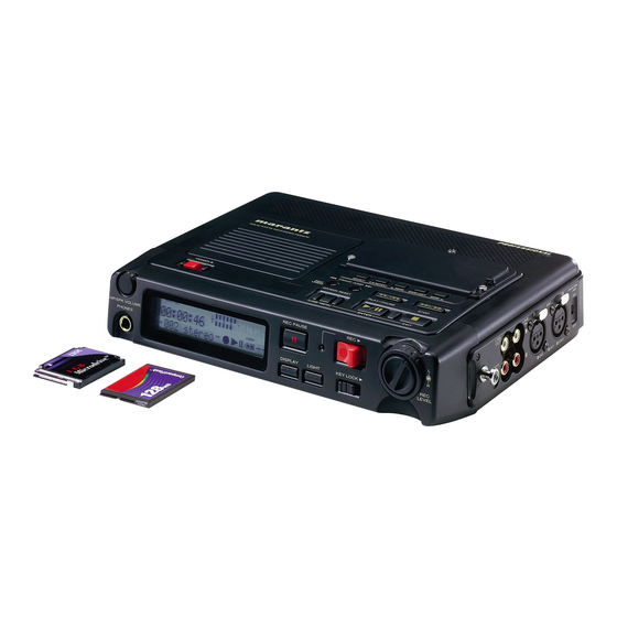
SOLID STATE RECORDER PMD670
POWER
3 2
1 0
TOTAL TRACK TIME
A-B
REC REMAIN kbps
HP/SPK VOLUME
kHz
AM
PHONES
PM
TRACK
MARK
TABLE OF CONTENTS
PMD670
PMD670 /
Solid State Recorder
STEREO
OFF
ON
L
R
0dB
-20dB
AUTO MARK
ANALOG OUT
MIC ATTEN
SINGLE
FLAT
ALL
OFF
ON
OFF
PRE REC
REPEAT
ANC
LIMITER
OFF
ON
OFF
ON
ALC
MANUAL
INPUT LOCK
EDL PLAY
LEVEL CONT.
EDIT
INPUT
A-B REPEAT
MARK
TRACK JUMP
-/REW
FWD/+
REC
UNDO
MARGIN RESET
PLAY/PAUSE
STOP
/
MENU/STORE
ENTER
CANCEL
6
REC PAUSE
REC
L
-dB
40
20
12
6
2
0
OVER
R
S.SKIP
-dB
INT
DISPLAY
LIGHT
KEY LOCK
MIC
LINE
W1B/U1B/F1B
MIC
5
4
L
R
REC
LEVEL
PAGE
Part no. 04AS855010
First Issue 2003.06
ecm
Advertisement
Table of Contents

Related Manuals for Marantz PMD670/W1B


Summary of Contents for Marantz PMD670/W1B
-
Page 1: Table Of Contents
Service PMD670 / W1B/U1B/F1B Manual Solid State Recorder STEREO -20dB AUTO MARK ANALOG OUT MIC ATTEN SOLID STATE RECORDER PMD670 SINGLE FLAT PRE REC REPEAT LIMITER MANUAL INPUT LOCK EDL PLAY LEVEL CONT. EDIT INPUT A-B REPEAT MARK TRACK JUMP -/REW FWD/+ UNDO... - Page 2 Parts for your MARANTZ equipment are generally available to our National Marantz Subsidiary or Agent. ORDERING PARTS : Parts can be ordered either by mail or by Fax.. In both cases, the correct part number has to be specifi ed.
-
Page 3: Technical Specifications
1. TECHNICAL SPECIFICATIONS Digital audio system Outputs System LINE OUT L/R Solid State recorder Type: RCA jack Usable Media Standard level: 2 Vrms max./2 kohms IC memory cards and HDD(Micro Drive) cards DIGITAL OUT Recording and reading method Type: RCA jack MPEG1 Layer 2/3 compression Output impedance: 75 ohms 16 bit linear PCM... -
Page 4: Factory/Service Mode
2. FACTORY/SERVICE MODE A. FACTORY MODE To reset all settings to default status ,follow the procedure below. 1. When Power Standby mode, While pressing A-B REPEAT and INPUT buttons, Slide POWER switch to turn on the unit. 2. FACTORY name is displayed on LCD. The unit becomes the setup of default automatically. -
Page 5: Lcd Contrast Adjustment
3. LCD CONTRAST ADJUSTMENT 1. Connect the TEST POINT (See below) with the tester. 2. Turn the variable resistor RF01(RF09) so that the reading of the tester becomes 7.0 V ± 0.1 V and conferm the contrast of the LCD becames maximum. 4. - Page 6 4) Remove 2 screws from both sides as shown in Fig.3 and Fig.4. <Fig.3 Po si tion of screw> <Fig.4 Position of screw> 5) Remove the front panel, holding it and pushing down with thumb as shown in Fig.5 and Fig.6. Cautions : When removing the front panel, take care not to damage the cable and connectors.
- Page 7 7) Remove 5 connectors as shown in Fig.8. And remove the top case. <Fig.8 Position of connectors> 8) Remove 4 connectors as shown in Fig.9. <Fig.9 Position of 4 connectors> 9) Remove 5 screws. Then remove side panel of Audio I/O side. <Fig.10 Position of 5 screws>...
- Page 8 10) Remove 6 screws. Then remove side panel of CompactFlash side. <Fig.11 Position of 6 screws> 11) Remove 7 screws. Then remove the PCB. <Fig.12 Turning over the Main PCB> <Fig.12 Position of 7 screws>...
-
Page 9: Dsp(Qd01) Firmware Update Procedure
5. DSP(QD01) FIRMWARE UPDATE PROCE- DURE Necessary Equipment • Windows PC((Windows20 or WindowsXP) • USB cable (USB 4Pin - mini USB 5pin) • CompactFlash (with format) • Update Disc (*PMD670CDR) Connection 1. Connect Windows PC and PMD670 with USB cable 2. - Page 10 10. When the updatiing is fi nished, information of Compact- Flash is displayed on LCD. 11. Turn off POWER switch. The fi rmware has been updated. Do the next procedure. 12. Connect Windows PC and PMD670 with USB cable 13. Repeat the same procedure No1., No2. and No3. 14.
-
Page 11: Main Microprocessor (Qu01) Update Procedure
6. MAIN MICROPROCESSOR (QU01) UPDATE PROCEDURE Necessary Equipment • Flash Writer (FLASH2 Disc and Parallel cable are packed together) • JIG PCB with the cable(5 pin USB mini cable) RS232C cable (25pin-9Pin ) • • Update Disc ( *PMD670CDR Windows PC (Windows2000 or WindowsXP) with COM •... - Page 12 Start Installation . Click Next Click Next (when you must change the installation Folder, Select the Folder ) Click Next...
- Page 13 The screen becomes the installation condition. Click Close Installation was completed in the PC. The icon of Flash2 is made in the desk-top computer. Confi guration Connect AC adapter to PMD670 and turn off (power standby mode) the unit. Confi rm the connection of the PMD670, Flash Writer and the PC.
- Page 14 Select H8/3048B from CPU type Click OK Click Set from Menu bar. Select COMMUNICATION Select Transfer rate in boot-mode : 19200bps Select Max transfer rate : =boot Select Communication port : COMx (Select the same COM Port number that the RS232C cable is connected.) Click OK Click Set...
- Page 15 Click Set from Menu bar. Select Terminal State Select High or Low from Setting Terminal State MD0: High MD1: I /O0: High I /O1: High I /O2: High FWE: High Click OK Finish Confi guration, the next process starts uploading. Writing Insert the update disc (part no : *PMD670CDR) in to CD-R drive.
- Page 16 The screen becomes the uploading condition. Verifl ing is started when writing is fi nished. Click OK The upload procedure is completed. Disconnect USB cable from the PMD670, then turn off POWER switch. Check the version number of the fi rmware Refer to 2-page "SERVICE MODE"...
-
Page 17: Wiring Diagram
7. WIRING DIAGRAM SPEAKER PF01... -
Page 18: Block Diagram
8. BLOCK DIAGRAM DC-DC POWER SUPPLY and BATTERY CHARGER LCD DRIVER LCD DISPLAY DC13V or BATT. KEY PANNEL NJU6469 DCIN +3.3V +3.3V VF01 +48V for uP for DSP QF01 +1.6V +-7V for DSP POWER ON/OFF BATTERY MONITOR POWER LED BATTERY CHARGE CHARGE LED REC LED EEPROM... -
Page 19: Schematic Diagram
9. SCHEMATIC DIAGRAM L404 PM01-1/10 +3VD R442 BLM11B601 MAIN PCB C424 C414 C416 10/10V 100n 470n CODEC_ADIN CODEC_ADIN CODEC_WS R429 CODEC_WS R425 +3VD 18k% +3VD CODEC_BCLK R421 CODEC_BCLK CODEC_DACOUT CODEC_DACOUT C437 R430 DAI_IN DAI_IN R440 L403 R426 INT0 INTERFACE FOR DSP C440 AVSS C439... - Page 20 PS01 POWER SW PCB PM01-2/10 PP01 +3VU SU03 SSST01-3A PHANTOM SW +3VD +3VU MAIN PCB POWER JU07 SWITCH RU17 B10B-PH-SM3 +3VU 100k SU01 SSAA22-B B3B-PH JU04 JU01 RU56 RU57 RU58 S3B-PH RU09 RU14 100k MD 2 JU03 JU10 QU02 CU16 BD4719G +3VU N.C.
- Page 21 PM01-3/10 RX16 +3VD MAIN PCB QX07 DTC114EU CF_INTRQ DSP_INT3 CF_IORDZ CF_IORDZ CF_IOWRZ CF_IOWRZ CF_CS0Z CF_CS0Z JX01 CF_CS1Z CF_CS1Z CON50_CF CF_CD1Z CF_CD1Z CF_CD2Z CF_DATA3 DATA3 CF_CD2Z CF_DATA4 DATA4 CF_DATA5 DATA5 BUS BUFFER QX03 74LCX541 CF_DATA6 DATA6 CF_DATA7 CX01 DATA7 CF_CS0Z /CS0 ADDR10 CX17 /ATA_SEL...
- Page 22 PM01-4/10 DATA3 MAIN PCB TPP5 DATA3 CF_INSZ CF_INSZ CF_CD2Z CF_CD2Z DM:Dumm y CF_CD1Z CF_CD1Z DATA2 +3VD DATA2 CP06 RP11 100n DATA1 RP19 +3VD DATA1 BLM601 JP01 DATA0 DATA0 ADDR13 ADDR13 ADDR14 ADDR14 RP15 ADDR15 ADDR15 BLM11B601 CODEC_BCLK ADDR19 ADDR19 CODEC_WS ADDR20 ADDR20 RP16...
- Page 23 PM01-5/10 MAIN PCB HBIL HBIL CD01 HDS1Z 100n RD05 HDS1Z +3VD HR/WZ HR/WZ QD02 HCSZ M29W800AB HCSZ +3VD +1.6VD TP13 HRDY ADDR0 DATA0 HRDY ADDR1 DATA1 DSP_RSTZ ADDR2 DATA2 DSP_RSTZ HCNTL0 ADDR3 DATA3 HCNTL0 HCNTL1 Flash ADDR4 DATA4 HCNTL1 ADDR5 DATA5 ADDR6 DATA6...
- Page 24 AVSW AVSW DVSW DVSW PM01-6/10 CHARGE_ON H:ANALOG POWER ON H:DIGITAL POWER ON CHARGE_ON BATT_DET MAIN PCB BATT_DET ACIN Q804 L801 ACIN 2SA1797 D813 L804 NLF3225 RB160L NLF3225 +3VU PD_MUTE 47uH 10uH C838 C833 PD_MUTE Q817 DTA114EU 100n C856 C855 100n 47/4V 47/4V +3VSTB...
- Page 25 VF01 LCD UNIT PF01 FRONT PCB 9 10 11 12 13 14 15 16 17 18 19 20 21 22 23 24 25 26 27 28 29 30 31 32 33 34 35 36 37 38 39 40 41 42 43 44 45 46 47 48 49 50 51 52 53 54 55 56 57 58 59 60 61 62 63 64 65 66 67 68 69 70 71 72 73 74 75 JF01 19FMN-BMTTN +5VD...
- Page 26 PM01-7/10 P001-2/3 AUDIO I/O PCB MAIN PCB RA06 100k JA03 NC3FAH2 MIC/LINE INPUT CA04 RA01 CA05 JA04 COLD B6B-PH-SM3 100n RA77 RA02 Rch Normal CA03 RA14 CA50 CA01 CA06 10/10V RA69 RA79 10/10V Int.MIC 10/10V RA05 QA13 Rch Invert JA05 RA46 RA04 DTC323TU...
- Page 27 PM01-8/10 QB01 MAIN PCB NJM022V CB35 10/10V RB28 AL_IN RB35 CB30 100k RB29 100n FROM PM01-10/10 CB33 CB03 100p 100n CB37 10/10V CB01 100p RB06 RB31 RB01 AR_IN RB37 RB04 100k QB01 CB04 RB32 NJM022V QB07 NJM022V 100n RB02 RB05 CB05 10/10V CB02...
- Page 28 P003 PM01-9/10 RC05 REC VOL. PCB RC31 CC03 MAIN PCB RC64 QC02 CC07 10/10V REC VOL ANALOG_L CC36 10/10V QC01 RC07 CC01 NJM022V 100k TO PM01-1/10 QC06 RC01 RC03 CC05 NJM022V 10/10V CC42 100n RC59 100K 100n ANALOG_R RC06 CC04 RC32 CC11 JC02...
- Page 29 R309 PM01-10/10 C306 C303 C309 100n MAIN PCB C302 100n Q303 R301 100n NJM022V R304 R366 (CPU) R305 C312 L307 R302 BLM11B102 R303 C304 R316 R318 R319 10/10V R314 100k C301 100k C305 Q310 C315 Q306 R322 DTC114TE 100n NJM4556M GND GND R313 R307...
- Page 30 PF02 BPF FLAT HPF RF51 OPERATION PCB 0dB -20dB SF71 SF70 MIC ATT DF51 1SS176 DF58 1SS176 STOP SF55 SF51 SF58 SF62 SF66 INPUT EDL PLAY DF61 DF65 DF69 REPEAT0(Single) CHANGE/LOCK STOP OFF/ON MENU 1SS176 1SS176 1SS176 DF54 DF59 9 10 1SS176 1SS176 PLAY...
-
Page 31: Parts Location
10. PARTS LOCATION P003 PW06 PS01 PP01 PH01 PF02 PF01 A P001 PF01 B QF02 QF04 QF03 QF01 P801 PC01... - Page 32 C309 C6 CC11 D9 L813 C4 LU24 F8 Q318 B7 QA02 B8 QC23 D8 R334 C6 R414 D7 R806 B1 R851 B1 R906 C5 RA39 B8 RB12 C8 RC45 D8 RD17 E5 RP25 D5 RX48 F4 TP41 D7 C310 C6 CC12 D9 LD01 E5 LU25 F8...
- Page 33 C301 C343 C418 C443 C835 CA20 CB04 CC26 CP06 CX07 D802 L301 LX04 Q332 Q821 Q847 QC15 QX03 R320 R360 R403 R437 R828 R871 R902 RC35 C302 C344 C419 C805 C836 CA21 CB12 CC33 CU05 CX08 D803 L305 LX04 Q333 Q822 Q848 QC16...
-
Page 34: Microprocessor And Ic Data
11. MICROPROCESSOR AND IC DATA QU01 : 64F3048BVF25(FRONT uP) Port Name I/O USE Sig. Name PUP Description Port Name I/O USE Sig. Name PUP Description +3.3V SCAN6 OFF Key scan TIOCA3 Buzzer SCAN7 OFF Key scan HBIL For DSP KEYIN0 Key scan TIOCA4 REC LED... - Page 35 QX01:GL641USB Pin No. Name Description Mic ro - PVDD Power supplier for storage device co ntroll er interface Storage device data bus bit 8* Storage device data bus bit 9* Endpoi nt 0 Storage device data bus bit 10* Contro l 8 Bytes FIFO Storage device data bus bit 11* PGND...
- Page 36 Q401 : AK4114 DIT Pin Name Function IPS0 Input Channel Select 0 Pin in Parallel Mode Receiver Channel 4 Pin in Serial Mode (Internal biased pin) No Connect NC(AVSS) No internal bonding. This pin should be connected to AVSS. DIF0 Audio Data Interface Format 0 Pin in Parallel Mode Receiver Channel 5 Pin in Serial Mode (Internal biased pin) TEST 2 pin...
- Page 37 Q401 : AK4114 DIT Pin Name Function Power-Down Mode Pin When “L”, the AK4114 is powered-down and reset. Master Clock Operation Mode 0 Pin in Parallel Mode CDTO Control Data Output Pin in Serial Mode, IIC= “L”. CAD1 Chip Address 1 Pin in Serial Mode, IIC= “H”. Master Clock Operation Mode 1 Pin in Parallel Mode CDTI Control Data Input Pin in Serial Mode, IIC= “L”.
- Page 38 Q402:AK5380VT AGND DGND MCLK Clock Divider ∆∑ Decimation AINL Modulator Filter LRCK SCLK ∆∑ Decimation AINR Modulator Filter Serial I/O SDTO Interface VCOM Voltage Reference Pin Name Description AINR Rch Analog Input Pin AINL Lch Analog Input Pin NC Pin No internal bonding.
- Page 39 Q403:AK4380VT-E2 MCLK Clock De-emphasis SMUTE/CSN µP Control Divider VCOM DFS/CCLK Interface DIF0/CDTI AOUTL Modulator Audio Interpolator LRCK Data BICK Interface SDTI AOUTR Interpolator Modulator VREF...
- Page 40 QP01:XC9536XL-VQ64-10C JTAG In-System Programming Controller JTAG Port Controller Function Block 1 Macrocells 1 to 18 Function Block 2 Macrocells 1 to 18 Blocks I/O/GCK I/O/GSR I/O/GTS QD03/QD04:M68AW256M70ND1 QD02:M29W800AB80N5 A0-A17 Address Inputs V CC V CC DQ0-DQ15 Data Input/Output Chip Enable Output Enable A0-A17 DQ0-DQ15...
- Page 41 QX02/QX04/QX05 : MC74LVX245DT QX03 : MC74LVX541DT MC74LVX541 LOGIC DIAGRAM DATA NONINVERTING INPUTS OUTPUTS OUTPUT ENABLES PIN ASSIGNMENT FUNCTION TABLE Inputs Output Y IEC LOGIC DIAGRAM &...
- Page 42 Q307/QA01/QA02/QA08/QB08:TC74HC4052AFT QB06/QC02/QC03:BU4053BCFV (Refer:HC4053A) Q305:NJM2070M...
- Page 43 Q819:BA9741FS-E2...
- Page 44 Q820 : NJM2373AF QF01 : NJU6469LFG1...
- Page 45 QD01 : TMS320VC5416PGE-160 Table 2–2. Signal Descriptions (Continued) Table 2–2. Signal Descriptions (Continued) TERMINAL TERMINAL TERMINAL TERMINAL I/O † I/O † I/O † I/O † DESCRIPTION DESCRIPTION DESCRIPTION DESCRIPTION NAME NAME NAME NAME The TMS320VC5416PGE 144-pin low-profile quad flatpack (LQFP) pin assignments are sh INITIALIZATION, INTERRUPT AND RESET OPERATIONS HOST-PORT INTERFACE SIGNALS Figure 2–2.
-
Page 46: Exploded View And Parts List
12. EXPLODED VIEW AND PARTS LIST VERS. POS. PART NO. PART NO. 5 1 1 0 DESCRIPTION 3 X 1 0 ( U) COLOR (FOR EUR) (MJI) 5 1 2 8 1 5 0 B 2 . 6 X 8 ( U) 001B 04AS248500 FRONT PANEL K 04AS248500... -
Page 47: Electrical Parts List
13. ELECTRICAL PARTS LIST NOTE ON SAFETY FOR FUSIBLE RESISTOR : ASSIGNMENT OF COMMON PARTS CODES. RESISTORS The suppliers and their type numbers of fusible resistors : 1) GD05 × × × 140, Carbon film fixed resistor, ±5% 1/4W are as follows; : 2) GD05 ×... - Page 48 SP01013370 CF04 EY47501670 TANTL. CHIP 4.7µF 16V EY47501670 SF69 EVQ11L05R H/5MM,160GF CF05 EY47501670 TANTL. CHIP 4.7µF 16V EY47501670 SF70 SS02021680 SLIDE SW. SSSF022-S06N0 ATT SS02021680 NOTE : "nsp" PART IS LISTED FOR REFERENCE ONLY, MARANTZ WILL NOT SUPPLY THESE PARTS.
- Page 49 CER. CHIP 2200pF (GR39) DK96222300 C351 EY10601070 TANTL. CHIP 10µF 10V EY10601070 C822 CER. CHIP 0.01µF ±10% 50V DK96103300 C357 CER. CHIP 47pF ±5% CG 50V DD95470300 C1608JB1H103K NOTE : "nsp" PART IS LISTED FOR REFERENCE ONLY, MARANTZ WILL NOT SUPPLY THESE PARTS.
- Page 50 10µF 10V EY10601070 CB23 CER. CHIP 0.1µF ±10% 50V DK96104300 CA10 CER. CHIP 0.1µF ±10% 50V DK96104300 C1608X7R1H104K C1608X7R1H104K CB24 EY10601070 TANTL. CHIP 10µF 10V EY10601070 NOTE : "nsp" PART IS LISTED FOR REFERENCE ONLY, MARANTZ WILL NOT SUPPLY THESE PARTS.
- Page 51 CER. CHIP 0.1µF ±10% 50V DK96104300 CD10 CER. CHIP 1µF 10V F DK98105200 C1608X7R1H104K CD11 CER. CHIP 1µF 10V F DK98105200 CX15 EY10601070 TANTL. CHIP 10µF 10V EY10601070 NOTE : "nsp" PART IS LISTED FOR REFERENCE ONLY, MARANTZ WILL NOT SUPPLY THESE PARTS.
- Page 52 NN05221610 R366 CHIP 10kΩ ±5% 1/16W NN05103610 R820 CHIP 100kΩ ±5% 1/16W NN05104610 R367 CHIP 100kΩ ±5% 1/16W NN05104610 R821 CHIP 220Ω ±5% 1/16W NN05221610 NOTE : "nsp" PART IS LISTED FOR REFERENCE ONLY, MARANTZ WILL NOT SUPPLY THESE PARTS.
- Page 53 RA53 CHIP 180Ω ±5% 1/16W NN05181610 R899 NI01103110 CHIP 10kΩ ±1% 1/10W NI01103110 RA54 CHIP 180Ω ±5% 1/16W NN05181610 RA55 CHIP 180Ω ±5% 1/16W NN05181610 NOTE : "nsp" PART IS LISTED FOR REFERENCE ONLY, MARANTZ WILL NOT SUPPLY THESE PARTS.
- Page 54 NN05103610 RD34 FC90020110 FERRITE CHIP BLM11B601S FC90020110 RC18 CHIP 10kΩ ±5% 1/16W NN05103610 RC19 CHIP 1kΩ ±5% 1/16W NN05102610 RP01 CHIP 1MΩ ±5% 1/16W NN05105610 NOTE : "nsp" PART IS LISTED FOR REFERENCE ONLY, MARANTZ WILL NOT SUPPLY THESE PARTS.
- Page 55 BA10026210 DIG.TRS. DTA114EU BA10026210 D302 HZ21005000 CHIP DIODE 1SS301,DAN202U HZ21005000 Q327 BA10026210 DIG.TRS. DTA114EU BA10026210 D303 HZ21005000 CHIP DIODE 1SS301,DAN202U HZ21005000 Q328 BA20035210 DIG.TRS. DTC114EU BA20035210 NOTE : "nsp" PART IS LISTED FOR REFERENCE ONLY, MARANTZ WILL NOT SUPPLY THESE PARTS.
- Page 56 HC010717K0 IC MC74LVX245DT HC010717K0 2SC4081 (Q,R) 2SC4116 (Y,GR) QX06 HX117971A0 CHIP TRS. 2SA1797 HX117971A0 Q852 HX117971A0 CHIP TRS. 2SA1797 HX117971A0 QX07 BA20035210 DIG.TRS. DTC114EU BA20035210 NOTE : "nsp" PART IS LISTED FOR REFERENCE ONLY, MARANTZ WILL NOT SUPPLY THESE PARTS.
- Page 57 FN31010030 EMIFILTER BLM11B102S 1608 FN31010030 LU25 FN31010030 EMIFILTER BLM11B102S 1608 FN31010030 LU26 FN31010030 EMIFILTER BLM11B102S 1608 FN31010030 LU27 CHIP RES. 1kΩ ±5% 1/16W NN05102610 LU32 NOTE : "nsp" PART IS LISTED FOR REFERENCE ONLY, MARANTZ WILL NOT SUPPLY THESE PARTS.
Need help?
Do you have a question about the PMD670/W1B and is the answer not in the manual?
Questions and answers