Kenwood NX-5400 Service Manual
700/800mhz digital transceiver
Hide thumbs
Also See for NX-5400:
- Common function reference (476 pages) ,
- Function reference (190 pages) ,
- User manual (80 pages)
Table of Contents
Advertisement
700/800MHz DIGITAL TRANSCEIVER
B5B-7155-00
9 S ERVICE MANUAL
2014
RA016<Rev.001>
COPYRIGHT © 2014 JVC KENWOOD Corporation
1
Precaution. . . . . . . . . . . . . . . . . . . . . . . . . . . . . . . . . . . . . . . . . . . . . . . . . . . . . . . . . . . . . . . . . . . . . . . . . 1-4
2
Specific Service Instructions . . . . . . . . . . . . . . . . . . . . . . . . . . . . . . . . . . . . . . . . . . . . . . . . . . . . . . 1-4
3
Disassembly . . . . . . . . . . . . . . . . . . . . . . . . . . . . . . . . . . . . . . . . . . . . . . . . . . . . . . . . . . . . . . . . . . . . . . 1-23
4
Adjustment . . . . . . . . . . . . . . . . . . . . . . . . . . . . . . . . . . . . . . . . . . . . . . . . . . . . . . . . . . . . . . . . . . . . . . . 1-29
5
Troubleshooting . . . . . . . . . . . . . . . . . . . . . . . . . . . . . . . . . . . . . . . . . . . . . . . . . . . . . . . . . . . . . . . . . 1-64
This product complies with the RoHS directive for the European market.
B5B-7155-00
SERVICE MANUAL
NX-5400 F2,K2
Note :
Lead free solder used in the board (material : Sn, Ag, In, Bi, melting point : 227 Centigrade)
COPYRIGHT © 2014 JVC KENWOOD Corporation
NX-5400
NX-5400 F3,K3
TABLE OF CONTENTS
This product uses Lead Free solder.
No.RA016<Rev.001>
2014/9
Advertisement
Table of Contents

Related Manuals for Kenwood NX-5400


Summary of Contents for Kenwood NX-5400
- Page 1 B5B-7155-00 NX-5400 NX-5400 F2,K2 NX-5400 F3,K3 COPYRIGHT © 2014 JVC KENWOOD Corporation Note : Lead free solder used in the board (material : Sn, Ag, In, Bi, melting point : 227 Centigrade) TABLE OF CONTENTS PRECAUTION............... . . 1-4 SPECIFIC SERVICE INSTRUCTIONS .
- Page 2 Neither is any liability assumed for damages resulting from the use of the information contained herein. JVC KENWOOD Corporation reserves the right to make changes to any products herein at any time for improvement purposes. Firmware Copyrights The title to and ownership of copyrights for firmware embedded in KENWOOD product memories are reserved for JVC KENWOOD Corporation.
- Page 3 Less than 2% Modulation 16K0F3E, 14K0F3E, 11K0F3E, 8K10F1E, 8K10F1D, 8K10F1W, (8K30F1E, 8K30F1D, 8K30F7W, 4K00F1E, 4K00F1D, 4K00F7W, 4K00F2D) Measurements made per TIA/EIA-603 and specifications shown are typical. JVC KENWOOD Corporation reserves the right to change specifications without prior notice or obligation. (No.RA016<Rev.001>)1-3...
- Page 4 This service manual does not describe PRECAUTION. SECTION 2 SPECIFIC SERVICE INSTRUCTIONS SYSTEM SET-UP Merchandise received Frequency range (MHz) RF power Type DTMF keypad 763~775.99375 NX-5400 F2 793~805.99375 806~825 NX-5400 F3 851~870 Choose the type of transceiver NX-5400 K2 763~775.99375 NX-5400 K3 851~870...
- Page 5 The latest version of the USB driver is available for download 2.2.3 Panel Test Mode from the following URL: Setting method refer to ADJUSTMENT. http://www.kenwood.com/usb-com/ (This URL may change without notice.) 2.2.4 Panel Tuning Mode Setting method refer to ADJUSTMENT.
- Page 6 LCD. 2.2.6.3 Programming Each press of the key shifts the display in order to the (1) Start up the firmware programming software (KENWOOD left. Firmware Loader). The KFL.exe exists in the KPG-D1/D1N When you enter the password and press [ ] or [*] key, installed holder.
- Page 7 The following setup items can be changed or added by us- ing the Front panel programming mode. • RX/TX Frequency • The setup items for Front panel programming mode are as • Channel Type follows. • Channel Spacing Setup item Display Remarks •...
- Page 8 Key\Item Zone Select Channel RX Frequency TX Frequency Channel Channel RX Signaling TX Signaling Select Type Spacing Keypad Unused Back to the Back to the pre- Back Back to the Back to the Back to the Back to the [#] *3 previous vious item previous item...
- Page 9 • Front panel programming mode flow chart Input Password Enter the Front panel programming mode Clone/Front Panel Password by using section "2.2.2 How to Enter Each Mode". Front panel Programming mode ] or [ Keep This Change? Zone Select ] or [ Channel Name Channel Select ] or [...
- Page 10 (G13-2179-XX) (G13-2178-XX) (G1D-0006-XX) (G1D-0055-XX) Note: Supplied accessories with * mark are not used for the NX-5400. 2.3.2 INSTALLING THE MODULE IN THE TRANSCEIVER ATTENTION: When installing the module, please take measures to prevent static electricity. (1) Remove the VOID sheet.
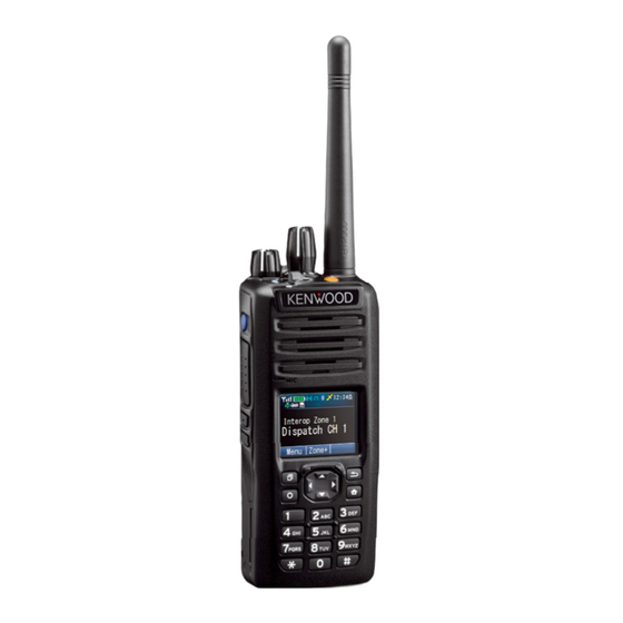
- Page 11 CIRCUIT DESCRIPTION 2.4.1 Overview The NX-5400 is a 700/800MHz FM & P25 Portable transceiver designed to operate in the frequency range of 763 to 775.99375MHz, 793 to 805.99375MHz (700M) and 806 to 825MHz, 851 to 870MHz (800M). The unit consists of a receiver, a transmitter, a phase-locked loop (PLL) frequency synthesizer, a digital control unit, and a power sup- ply circuit.
- Page 12 2.4.3.3 Audio Amplifier Circuit Audio processing (high-pass filter, low-pass filter, de-emphasized and so on) at FM mode and decoding at P25 mode are processed by DSP. SSI signal from DSP is converted to audio signal at IC902. The signal goes to amplifier (IC904 or IC905). While INTAMT is High, IC904 is activated and audio is heard from internal speaker.
- Page 13 2.4.5 PLL Frequency Synthesizer 2.4.5.1 TCXO (X700) TCXO (X700) generates a reference frequency of 19.2MHz for the PLL frequency synthesizer. This reference signal is buffered by Q700 and IC700. And it is distributed to TX PLL (IC100), RX PLL (IC200), IF IC (IC600), BT/GPS IC (IC850), and IC702. The frequency adjustment is achieved by adjusting a D/A converter (IC901) output in the voltage of the control terminal of TCXO.
- Page 14 2.4.6.5 Low Battery Warning The battery voltage is divided using R40 and R41 and is detected by A/D converter (IC900). When the battery voltage falls below the voltage set by the Low battery warning adjustment, the red LED blinks to notify the operator that it is time to replace the battery. If the battery voltage falls even more (approx.
- Page 15 (3.15A) Battery Final Amp, APC IC31 IC32 MPU/DSP RTC 31BU 12BU BackUp Battery SCM Board IC33 MPU/DSP Core, MPU/DSP PLL IC34 MPU/DSP 1.8V I/O, mDDR2, LCD Module I/O IC701 Flash ROM I/O, 18M_3 AudioCodec DVDD IC37 BT & GPS I/O 18BT IC38 BT &...
- Page 16 KEY Back Light, 3Color LED, IC82 8bit/16ch ADC, Universal I/F IC801 Universal Option IC36 PLL, IF, VCO IC60 ASSIST 200C IC360 ANTSW ANTSW IC63 50VCO Q110 TX VCO Q210 RX VCO IC65 TX circuit IC64 RX circuit 8bit ADC (1A) Int AF Amp 53AF Ext AF Amp...
- Page 17 2.4.9 Bluetooth/GPS Circuit The main component of the Bluetooth/GPS circuit is BT/GPS IC (IC850). The clocks of BT/GPS IC require 19.2MHz for core and 32.768kHz slow clock (X850) for UART. 19.2MHz clock (X700) is shared with MPU/DSP (IC702), and is supplied through the clock buffer IC (IC700). The BT/GPS IC communicates to the MPU/DSP (IC702) on the HCI UART.
- Page 18 2.4.9.2 GPS Circuit The RF signal is received by the antenna matched by the matching circuit. The matching circuit consists of L905, C948 and C883. And this signal applied to a high-pass filter. The filter consists of C882, C881, C880, L859 and L858. The filtered RF signal is then applied to a SAW filter (L857).
- Page 19 Ref. No. Part Name Description Ref. No. Part Name Description IC900 A/D converter Diode IC901 D/A converter Diode Overvoltage protection IC902 Codec Diode DC SW IC903 D/A converter Diode Backup battery charge IC904,905 IC Audio AMP Diode DC/DC converter IC906 Logic control D100 Zener diode...
- Page 20 Pin No. Name Function Pin No. Name Function - GND I/O LCD Data Bus 2 ENC2 I Rotary switch input I/O LCD Data Bus 1 ENC3 I Rotary switch input I/O LCD Data Bus 0 CNTSW I Lever switch input CABC I Backlight control signal - GND...
- Page 21 Pin No. Name Function CN13 O BTL output for internal speaker - O BTL output for internal speaker + DAT2 I/O Data 2 CD/DAT3 I/O Data 3 I/O Command input/output O 3.3V output O Clock output - GND DAT0 I/O Data 0 DAT1 I/O Data 1 I Card detect switch...
- Page 22 Rating and Condition Pin No. Name I/O Signal Type Function Parameter Min Typ Unit - Power 5V power supply output Output Voltage(Iout = 100mA) 4.9 5.0 Maximum Current O Digital Serial data output VOH(Io=-5mA) VOL(Io=5mA) Baud Rate 1.1875 Mbps USB_DP IO Analog USB DP Baud Rate (Full-Speed)
- Page 23 SECTION 3 DISASSEMBLY Precautions for Waterproof (2) Remove the selector knob spring <2>. • Do not remove the black sheet from the reverse side of the Note: transceiver (refer to the illustration below). Removal of this Use minimal contact with your fingers on the knob sheet decreases the waterproof efficiency of the transceiver spring.
- Page 24 <3> <3> • Regarding VOID, confirm the service policy of the NX- (4) Remove the LCD shielding case from the Main unit. <4> 5400 to KENWOOD (or authorized distributor). <1> <1> VOID seal 3.2.5 Remove the holder ASSY from the chassis (1) Remove the two hooks on the holder ASSY from the chas- sis.
- Page 25 (4) Remove the six screws <6>. 3.2.9 Removing the stopper of the selector circle nut and volume circle nut Note: (1) Remove the stopper <1> using a pair of tweezers. When you remove two screws (black), the battery termi- nal block is removed. <1>...
- Page 26 (4) Move the selector and volume switches and then remove Note: them both from the holes in the chassis. Perform the following procedures when you reassemble the shield cover. (1)Push evenly on the top cover and be careful that you do not bend it as you install it on a new shield cover.
- Page 27 (6) Press the packing evenly to the base of the chassis. (3) Insert the universal connector FPC into the connector (CN12). <3> Note: (4) Insert the PTT FPC into the connector (CN8). <4> To prevent doing any damage, do not press forcefully on (5) Insert the VOL/SEL/MIC FPC into the connector (CN4).
- Page 28 Main Parts Assembled Sheet/ Cushion Part Name Part Number Part Name Part Number Remark Plastic Cabinet (F3,K3) A0C-0001-00 Badge B4D-0002-00 “KENWOOD” is printed. Plastic Cabinet (F2,K2) A0C-0002-00 Fibrous Sheet (SP) G1A-0001-00 Sheet (LCD) G1B-0074-00 Spacer (2CH) J3K-0003-00 Knob (2CH) K2K-0013-00...
- Page 29 SECTION 4 ADJUSTMENT Controls Power switch/Volume control Selector knob Auxiliary (orange) key Transmit/ Receive/ Battery low indicator Lever switch Side 1 key PTT (Push To Talk) switch Universal connector Side 2 key Side 3 key 4.1.1 Preparations for checking/tuning the transceiver "FNC"...
- Page 30 "FNC" appears on the sub LCD display "FNC" appears on the sub LCD display Function Display Function Display Function off [Selector] Compander on/off icon appears Talk Around on/off icon appears Function off Analog/Phase1/Phase2/ Analog: "A" NXDN P25 phase1: "P1" [AUX For production P25 phase2: "P2"...
- Page 31 (2) Test signaling Analog mode signaling STTP-OB-1031 Symmetrical STTP-IB1031-1 None None Tone Pattern STTP-IB1031-1 (Half rate) None Square Wave Silence Pattern STP-IB-1 + LTR Data LTR Data (Half Rate) Silence Pattern (Half Rate) QT:67.0Hz QT:67.0Hz Audio Test Pattern STTP-IB1031-1 + Audio Test QT:151.4Hz QT:151.4Hz (Half Rate)
- Page 32 4.3.2 Key operation RSSI Reference, Open Squelch, Low RSSI, High RSSI, Tight Squelch Function Tuning point Display RX (MHz) TX (MHz) Push Hold (1 second) 700M RX/TA 700M RX/TA 763.100000 763.000000 [Selector] - Adjustment value up Continuation up 700M RX/TA 700M RX/TA 769.100000 769.000000...
- Page 33 Adjustment Item Description Adjustment Item Description High Transmit High Transmit Power is adjusted. QT Deviation QT deviation is adjusted. Power DQT Deviation DQT deviation is adjusted. Medium Transmit Medium Transmit Power is adjusted. RSSI Reference The minimum RSSI level for scan stop is Power adjusted.
- Page 34 Order Adjusutment Main Sub LCD Adjust item display (Analog (Analog (Analog (P25 (P25 (NXDN (NXDN item display Wide 5k) Wide 4k) Narrow) Phase1) Phase2) Nar- Very Number row) Nar- row) Adjustment range H-CPM P2DEV Transmitter Deviation Section 9 1~1024 NXDN High NDEV Transmitter...
- Page 35 4.3.6 Panel tuning mode flow chart Note: * In this Panel tuning mode flow chart, the Adjustment item name is modified. Adjustment Item N/W/VN Panel Test Mode LCD Display For all adjustment items, press the [ ] key QT Deviation to write the adjustment value.
- Page 36 BER (Bit Error Rate) Measurement (1) The Panel Test Mode is used to measure the BER (Refer "4.2.1 Test mode operation features"). (2) Select "10" (P25 Phase1), "7" (P25 Phase2) and "7" (NXDN Mode) for test signaling (Refer to "4.2.3 Frequency and Signaling"...
- Page 37 Nut wrench In order to turn the volume nut and the channel selector nut, use a recommendation tool. KENWOOD part No.: W05-1123-00 Battery Jig (W3F-0001-00) Connect the power cable properly between the battery jig installed in the transceiver and the power supply, and be sure output voltage and the power supply polarity prior to switching the power supply ON, otherwise over voltage and reverse connection may damage the transceiver, or the power supply or both.
- Page 38 *PC tuning 100 10V PCB layout Connect the wires to the PCB in the connector case of interface cable. AF Voltmeter 100 10V For output the wires out of the connector case, need to process the connector case. 10 10V KPG-36U Audio generator Shield...
- Page 39 Item Condition Measurement Adjustment Specifica- tions Panel test PC test mode Test- Unit Terminal Unit Parts Method /Remarks mode equipment 2-3. 1)CH-Sig: 7-1 1)Test Channel Power Panel ANT Check 2.5W~3.5W High PTT: ON Channel: 7 meter 2.2A or less power TA: OFF Test Signaling Mode: Analog Ammeter...
- Page 40 Item Condition Measurement Adjustment Specifica- tions Panel test PC test mode Test- Unit Terminal Unit Parts Method /Remarks mode equipment 3-2. 1)CH-Sig: 1-1 1)Test Channel Power Panel ANT Check 0.5W~1.5W PTT: ON Channel: 1 meter 1.4A or less power TA: ON Test Signaling Mode: Analog Ammeter check...
- Page 41 Item Condition Measurement Adjustment Specifica- tions Panel test PC test mode Test- Unit Terminal Unit Parts Method /Remarks mode equipment 5-1. 1)CH-Sig: 2-1 1)Test Channel Panel ANT Check 12dB SINAD Sensitivity SSG output Channel: 2 AF VTVM Universal or more check Wide 5k: Test Signaling Mode: Analog...
- Page 42 Item Condition Measurement Adjustment Specifications /Remarks Panel tuning PC test mode Test- Unit Ter- Unit Parts Method mode equip- minal ment 1) Adj item: [Manual Adjustment] Panel [Panel [PC test mode] 2.5V±0.1V Receive [RAST] 1) Adj item: tuning [Automatic Adjust- [Automatic Ad- Assist Adjust:[****]...
- Page 43 Item Condition Measurement Adjustment Specifications /Remarks Panel tuning PC test mode Test- Unit Ter- Unit Parts Method mode equip- minal ment *The Frequen- 1) Adj item: Panel ANT Panel [Panel [PC test mode] [PC test mode] Frequency cy adjust- [Frequency] tuning Press [Start] button of “IF20”...
- Page 44 Item Condition Measurement Adjustment Specifica- tions Panel tuning PC test mode Test- Unit Ter- Unit Parts Method /Remarks mode equip- minal ment 1) Adj item: 1) Adj item: Power Panel Panel [Panel [PC test mode] Ramp [RAMPD] [Ramp Down Off- meter tuning 1) Set the adjustment...
- Page 45 [TX Low]→ [TX High] (Same as TK-5400, the adjustment [TX High] [Frequency: old model of NX-5400). value after all [Frequency: 800MHz Band] Press [AUX(Orange)] adjustment 800MHz Band] [TX Low]→ key to switch the tone to points have [TX Low]→...
- Page 46 Item Condition Measurement Adjustment Specifica- tions Panel tuning PC test mode Test- Unit Ter- Unit Parts Method /Remarks mode equip- minal ment 1) Adj item: 1) Adj item: Devia- Panel ANT Panel [Panel Write fixed value “496” 4150~4250Hz Maxi- [Aw ADEV] [Maximum Devia- tion tuning...
- Page 47 Item Condition Measurement Adjustment Specifica- tions Panel tuning PC test mode Test- Unit Ter- Unit Parts Method /Remarks mode equip- minal ment [Analog 1) Adj item: 1) Adj item: Devia- Panel ANT Panel [Panel Write fixed value “488” 2050~2150Hz Narrow] [An ADEV] [Maximum Devia- tion...
- Page 48 Item Condition Measurement Adjustment Specifica- tions Panel tuning PC test mode Test- Unit Ter- Unit Parts Method /Remarks mode equip- minal ment 9. P25 1) Adj item: 1) Adj item: Devia- Panel ANT Panel [Panel Write fixed value “485” 3090~3215Hz H-CPM [P2 P2DEV] [P25 H-CPM Devi-...
- Page 49 Item Condition Measurement Adjustment Specifica- tions Panel tuning PC test mode Test- Unit Ter- Unit Parts Method /Remarks mode equip- minal ment [NXDN 1) Adj item: 1) Adj item: Devia- Panel ANT Panel [Panel Write fixed value “503” 1311~1363Hz Very [Nv NDEV] [NXDN High Devia- tion...
- Page 50 Item Condition Measurement Adjustment Specifica- tions Panel tuning PC test mode Test- Unit Ter- Unit Parts Method /Remarks mode equip- minal ment [Analog 1) Adj item: 1) Adj item: Devia- Panel ANT Panel [Panel Write the value as fol- 0.60kHz±0.05 Wide [As QT] [QT Deviation (An-...
- Page 51 Item Condition Measurement Adjustment Specifica- tions Panel tuning PC test mode Test- Unit Ter- Unit Parts Method /Remarks mode equip- minal ment 12. DQT 1) Adj item: 1) Adj item: Devia- Panel ANT Panel [Panel Write the value as fol- 0.75kHz±0.05 Devia- [Aw DQT]...
- Page 52 Item Condition Measurement Adjustment Specifica- tions Panel tuning PC test mode Test- Unit Ter- Unit Parts Method /Remarks mode equip- minal ment [Analog 1) Adj item: 1) Adj item: Devia- Panel ANT Panel [Panel Write the value as fol- 0.35kHz±0.05 Narrow] [An DQT] [DQT Deviation...
- Page 53 Item Condition Measurement Adjustment Specifica- tions Panel tuning PC test mode Test- Unit Ter- Unit Parts Method /Remarks mode equip- minal ment [Analog 1) Adj item: 1) Adj item: Devia- Panel ANT Panel [Panel Write the value as fol- 0.75kHz±0.05 Wide [As LTR] [LTR Deviation...
- Page 54 Item Condition Measurement Adjustment Specifica- tions Panel tuning PC test mode Test- Unit Ter- Unit Parts Method /Remarks mode equip- minal ment 1) Adj item: 1) Adj item: Devia- Panel ANT Panel [Panel Write the value as fol- 2.50kHz±0.05 DTMF [Aw DTMF] [DTMF Deviation tion...
- Page 55 Item Condition Measurement Adjustment Specifica- tions Panel tuning PC test mode Test- Unit Ter- Unit Parts Method /Remarks mode equip- minal ment [Analog 1) Adj item: 1) Adj item: Devia- Panel ANT Panel [Panel Write the value as fol- 1.25kHz±0.05 Narrow] [An DTMF] [DTMF Deviation...
- Page 56 Item Condition Measurement Adjustment Specifica- tions Panel tuning PC test mode Test- Unit Ter- Unit Parts Method /Remarks mode equip- minal ment [Analog 1) Adj item: 1) Adj item: Devia- Panel ANT Panel [Panel Write the value as fol- 2.40kHz±0.05 Wide [As MSK] [MSK Deviation...
- Page 57 Item Condition Measurement Adjustment Specifica- tions Panel tuning PC test mode Test- Unit Ter- Unit Parts Method /Remarks mode equip- minal ment 1) Adj item: 1) Adj item: Devia- Panel ANT Panel [Panel Write the value as fol- 1.00kHz±0.10 CWID [An CWID] [CWID Deviation tion...
- Page 58 4.9.1 Necessary Deviation adjustment item for each signaling and mode The following shows the necessary adjustment items for each signaling deviation. Please read the following table like the following example. In the case of the signaling “QT (Analog Wide 5k)”, this signaling is composed of three elements [Balance, Maximum Devi- ation (Analog Wide 5k) and QT Deviation (Analog Wide 5k)].
- Page 59 4.10 Receiver Section Item Condition Measurement Adjustment Specifi- cations Panel tuning mode PC test mode Test- Unit Ter- Unit Parts Method /Remarks equip- minal ment [Panel test mode] 1) Test Channel Panel ANT Panel Vol- Turn the Volume knob to 0.90V AF level 1) CH-Sig: 1-1...
- Page 60 Item Condition Measurement Adjustment Specifi- cations Panel tuning mode PC test mode Test- Unit Ter- Unit Parts Method /Remarks equip- minal ment [Analog 1) Adj item: 1) Adj item: Panel ANT Panel [Panel tuning mode] Wide [As SQL] [Open Squelch (An- Distor- Uni- After input signal from...
- Page 61 Item Condition Measurement Adjustment Specifi- cations Panel tuning mode PC test mode Test- Unit Ter- Unit Parts Method /Remarks equip- minal ment [P25 1) Adj item: 1) Adj item: Panel ANT Panel [Panel tuning mode] (LSM)] [P1 SQL] [Open Squelch (P25 Distor- Uni- After input signal from...
- Page 62 Item Condition Measurement Adjustment Specifi- cations Panel tuning mode PC test mode Test- Unit Ter- Unit Parts Method /Remarks equip- minal ment 1) Adj item: 1) Adj item: Panel ANT Panel [Panel tuning mode] [An LRSSI] [Low RSSI (Analog Uni- After input signal from RSSI Adjust:[***]...
- Page 63 Item Condition Measurement Adjustment Specifi- cations Panel tuning mode PC test mode Test- Unit Ter- Unit Parts Method /Remarks equip- minal ment [Analog 1) Adj item: 1) Adj item: Panel ANT Panel [Panel tuning mode] Wide [As SQLT] [Tight Squelch (Ana- Distor- Uni- After input signal from...
-
Page 64: Troubleshooting
SECTION 5 TROUBLESHOOTING Fault Diagnosis of the BGA (Ball Grid Array) IC Overview: A flowchart for determining whether or not the transceiver can be powered on (the LCD does not function even if the power switch is turned on) due to broken BGA parts. BGA parts: MPU/DSP (IC702), mobile DDR (IC703), Flash memory (IC705) When the BGA IC is problematic, please bring the printed circuit board (XC1-0321-81) in for service. - Page 65 When a normal Checking the output signal value is confirmed. from the MPU/DSP. When an abnormal If the IC706 (1 pin) is 0V or 1.8V, the MPU/DSP Normal voltage Points to be checked value is confirmed. may be broken. After power-on, and /CS_F IC706 (4 pin) If the IC706 (2 pin) is 0V or 1.8V, the MPU/DSP 1.8V...
- Page 66 Failure diagnosis of the GPS section Overview: When the GPS fuction does not operate, use this flowchart to determine the problem. Major parts for a GPS circuit GPS antenna (Connect on CN907) IC702 IC850 L857 Shee t metal IC852 LNA IC (IC851) UART UART Pre-SAW Filter (L857)
- Page 67 When a normal condition is confirmed. [The reference clock circuit When an abnormal When an abnormal Verify the reference clock for the BT/GPS. for the BT/GPS is faulty]. condition is confirmed. condition is confirmed. (BT_CLK) Intersection of Check the PCB side B (c). Verify the PCB side A parts C850 and R861: Sine waveform, C850, R861, R862.
- Page 68 [The GPS RF input circuit is faulty] Verify the RF input circuit for the GPS. When an abnormal Replace the GPS RF input circuit HPF, Pre-SAW, LNA, ATT, Post-SAW, condition is confirmed. parts. (only the parts which can be GPS IC RF Matching. replaced.) If any unexchangeable HPF parts: C882, C881, C880, L859, L858 parts are abnormal, replace the PCB.
- Page 69 Failure diagnosis of the Bluetooth section Overview: When the Bluetooth function does not operate, use this flowchart to determine the problem. Major parts for a Bluetooth circuit IC702 IC852 IC850 Bluetooth antenna (Connect on CN909) UART UART Shee t metal L855 Level LC filter (L855)
- Page 70 When a normal condition is confirmed. [The reference clock circuit Verify the reference clock for the BT/GPS. When an abnormal When an abnormal for the BT/GPS is faulty] (BT_CLK) Intersection of condition is confirmed. condition is confirmed. Verify the PCB side A parts Check the PCB side B (c).
- Page 71 Check the PCB side B (a). When a normal condition is confirmed. When an abnormal [The BT/GPS power supply line 33BT circuit is faulty] condition is confirmed. [The BT/GPS IC is abnormal] Verify the PCB side B parts. Replace the PCB. IC39, IC38, C55, L850 Replace any abnormal parts.
- Page 72 • The 0Ω resistor (R1) is used to differentiate the destina- tion with a visual check. These are not connected with any • When a new printed circuit board is used, the KENWOOD PCB pattern; they are specifically for production control.
- Page 73 SCHEMATIC DIAGRAM MAIN UNIT (XC1-0321-80) MAIN UNIT (XC1-0321-80) HDQ_1 HOLD_T OVER VOLTAGE PROTECTION VOLTAGE REGULATOR(50C) SDET RESET 7.46V 5.02V 20V DC/DC C114 IC36 DC-DC 7.48V 7.49V PLL_CLK R101 C105 7.49V FZA10BQ-3R15 XC6209B502D-G CONVERTER 100p CN301 3.15A BATT INT 18.8V 0.01u DC SW EMD12 DB2J40700...
- Page 74 BLOCK DIAGRAM MAIN UNIT (XC1-0321-80) IC702 --------------------------------------------------------- --CODEC(IC902)-- /CRST,MCLK,CODEC_DI,CODEC_D O --------------------------------------------------------- 700MHz: 763 775.99375MHz(RX/TX) --SD(J1)-- IC100 805.99375MHz(TX) SD1_DAT[0]~SD1_DAT[3],SD1_CLK,SD1_CMD,/SD_DE T SKY72310362LF 800MHz: 806 825MHz(TX) Q101 DSC9A01/T/ --------------------------------------------------------- 870MHz(RX/TX) Ripple D101 1SS400SM/T/ 50VCO 50VCO --UNIVERSAL CONNECTOR(CN12)- - Filter MIC_IESW,/EXT_PTT,/UDET,TXD1,RXD1,CTS1,RTS 1 IC102(1/2) IC712(2/2) BU7242NUX Q110 DDR_A[0]~DDR_A[13]...
-
Page 75: Printed Circuit Board
PRINTED CIRCUIT BOARD MAIN UNIT (XC1-0321-80) --- Component side view (J79-0414-09) --- CN31 R858 R859 L807 R806 C808 C807 C222 IC32 IC852 C223 IC853 Q800 R217 R745 CP851 C891 C806 C885 R746 L861 C889 IC705 L862 R331 C801 C859 Q210 C893 C856 C852... - Page 76 MAIN UNIT (XC1-0321-80) --- Foil side view (J79-0414-09) --- CP600 C603 L601 R162 C288 L600 R600 L602 C220 C880 C221 Q281 L857 C168 R291 C219 C615 C788 C283 C217 R182 R293 C611 L858 R281 C601 R214 R215 IC851 Q160 C291 C600 L180 C182...
- Page 77 A-1C ADDRESS TABLE OF BOARD PARTS Side Y axis Each address may have an address error by one X axis interval. REF.NO. LOCATION REF.NO. LOCATION REF.NO. LOCATION REF.NO. LOCATION REF.NO. LOCATION REF.NO. LOCATION REF.NO. LOCATION REF.NO. LOCATION REF.NO. LOCATION REF.NO. LOCATION REF.NO. LOCATION REF.NO. LOCATION REF.NO. LOCATION REF.NO. LOCATION REF.NO. LOCATION REF.NO. LOCATION REF.NO. LOCATION Q401 A- 4A A- 3A...
-
Page 78: Level Diagram
LEVEL DIAGRAM Receiver Section RF (Center Frequency) 1st IF (58.05MHz) AF (1kHz) - 119dBm - 120dBm - 121dBm - 123dBm - 109dBm - 110dBm - 112dBm - 115dBm - 116dBm - 105dBm - 102dBm 226mVp-p C544 L536 C540 Q530 C534 L530 C530 D350 D370 IC570... -
Page 79: Parts List
PARTS LIST [NX-5400] * SAFETY PRECAUTION Parts identified by the symbol are critical for safety. Replace only with specified part numbers. * BEWARE OF BOGUS PARTS Parts that do not meet specifications may cause trouble in regard to safety and performance. - Page 80 Exploded view of general assembly and parts list Block No.M1MM MAIN UNIT<01> 3-2(No.RA016<Rev.001>)
- Page 81 F2,K2 A8A-0005-00 REAR PANEL A1A-0005-00 CHASSIS B0K-0024-00 CAP(SD) B38-0960-05 LCD ASSY B4B-0006-00 CAUTION STICKER B4C-0105-00 TERMINAL STICKER B4D-0002-00 KENWOOD BADGE D32-0454-04 STOPPER(16CH) D3C-0001-10 STOPPER(CIRCULAR NUT) E04-0467-15 RF COAXIAL RECEPTACLE(SMA) E2D-0003-00 TERMINAL(ANT) E3H-0007-00 LEAD WIRE WITH CONNECTOR(SP) E58-0532-05 RECTANGULAR RECEPTACLE(14P) E7C-0001-00...
- Page 82 Symbol No. Part No. Part Name Description Local N14-1012-00 CIRCULAR NUT(RO-SW) N83-2005-48 PAN HEAD TAPTITE SCREW(UNIT/FIX) (x10) N84-2004-43 PAN HEAD TAPTITE SCREW(TERM-BL(+,-)) (x2) XC1-0321-81 SERVICE MAIN UNIT 3-4(No.RA016<Rev.001>)
-
Page 83: Electrical Parts List
Electrical parts list MAIN UNIT Symbol No. Part No. Part Name Description Local XC1-0321-80 KTA2012EP TRANSISTOR *Note1 : This part cannot be replaced. There- EM6M2 EM6M2 fore, this part is not supplied as a service part. LTC014EEBFS8 DIGI TRANSISTOR 2SB1132(Q,R) TRANSISTOR Block No. - Page 84 Symbol No. Part No. Part Name Description Local Symbol No. Part No. Part Name Description Local D703 RB521CM-30 DIODE CK73HBB1H681K C CAPACITOR 680PF K D704 NSSM038A CK73EB1H475KM C CAPACITOR 4.7UF K D705 RB521CM-30 DIODE CK73HB1A105K C CAPACITOR 1.0UF K D800 RB521CM-30 DIODE...
- Page 85 Symbol No. Part No. Part Name Description Local Symbol No. Part No. Part Name Description Local C191 CC73HCH1H050B C CAPACITOR 5.0PF B C340 C93-0974-05 C CAPACITOR 3.3PF G C192 CC73HCH1H1R5B C CAPACITOR 1.5PF B C341 CK73GXR1H104K C CAPACITOR 0.1UF K C200 CK73HB1H103K C CAPACITOR...
- Page 86 Symbol No. Part No. Part Name Description Local Symbol No. Part No. Part Name Description Local C574 C93-1959-05 C CAPACITOR 0.10UF K C673 CC73JCH1H101J C CAPACITOR 100PF J C580 CC73HCH1H180G C CAPACITOR 18PF G C674 CK73HBB1H102K C CAPACITOR 1000PF K C581 CC73HCH1H100B C CAPACITOR...
- Page 87 Symbol No. Part No. Part Name Description Local Symbol No. Part No. Part Name Description Local C772 C93-1959-05 C CAPACITOR 0.10UF K C857 C93-1959-05 C CAPACITOR 0.10UF K C773 CK73HB1A105K C CAPACITOR 1.0UF K C858 C93-1959-05 C CAPACITOR 0.10UF K C774 C93-1959-05...
- Page 88 Symbol No. Part No. Part Name Description Local Symbol No. Part No. Part Name Description Local C939 CC73HCH1H101J C CAPACITOR 100PF J RK73JB1H104J MG RESISTOR 100K J 1/20W C940 C93-1959-05 C CAPACITOR 0.10UF K RK73JB1H102J MG RESISTOR 1.0K J 1/20W C941 C93-1959-05 C CAPACITOR...
- Page 89 Symbol No. Part No. Part Name Description Local Symbol No. Part No. Part Name Description Local R205 RK73HB1J470J MG RESISTOR 47 J 1/16W R404 RK73HH1J472D MG RESISTOR 4.7K D 1/16W R206 RK73HB1J100J MG RESISTOR 10 J 1/16W R405 RK73HH1J472D MG RESISTOR 4.7K D 1/16W...
- Page 90 Symbol No. Part No. Part Name Description Local Symbol No. Part No. Part Name Description Local R703 RK73HB1J000J MG RESISTOR 0.0 J 1/16W R832 RK73HB1J101J MG RESISTOR 100 J 1/16W R704 RK73HH1J102D MG RESISTOR 1.0K D 1/16W R833 RK73HB1J101J MG RESISTOR 100 J 1/16W...
- Page 91 Symbol No. Part No. Part Name Description Local Symbol No. Part No. Part Name Description Local LB73H0AV-002 CHIP FERRITE BEADS L585 LK73H0AM33NJ SMALL FIXED INDUCTOR(33NH) L41-1502-70 SMALL FIXED INDUCTOR(15UH) L586 LB73H0AV-003 CHIP FERRITE BEADS LB73H0AV-002 CHIP FERRITE BEADS L587 LK73H0AM12NJ SMALL FIXED INDUCTOR(12NH)
- Page 92 Symbol No. Part No. Part Name Description Local E40-6962-05 FLAT CABLE CONNECTOR(35P) CN10 E40-6720-05 SOCKET FOR PIN ASSY(20P) CN11 E40-6720-05 SOCKET FOR PIN ASSY(20P) CN12 E41-3167-05 FLAT CABLE CONNECTOR(14P) CN13 E41-1486-05 PIN ASSY(2P) CN14 G0B-0005-00 EARTH SPRING CN15 G0B-0005-00 EARTH SPRING CN16 G0B-0005-00...
- Page 93 Packing materials and accessories parts list Block No.M2MM Packing and accessories Block No. [M][2][M][M] Symbol No. Part No. Part Name Description Local B0K-0002-00 B5A-0049-00 INSTRUCTION MANUAL ------------ PAMPHLET G5D-0027-00 PACKING ------------ PROTECTION BAG (60/110/0.07) ------------ PROTECTION BAG (100/250/0.07) H5A-0012-00 ITEM CARTON CASE J29-0730-05 BELT CLIP...
- Page 94 JVC KENWOOD Corporation Communications Equipment BU (No.RA016<Rev.001>) Printed in Japan...
Need help?
Do you have a question about the NX-5400 and is the answer not in the manual?
Questions and answers