ARM Cortex-M3 DesignStart User Manual
Hide thumbs
Also See for Cortex-M3 DesignStart:
- Technical reference manual (410 pages) ,
- Technical reference manual (400 pages)

Related Manuals for ARM Cortex-M3 DesignStart


Summary of Contents for ARM Cortex-M3 DesignStart
- Page 1 Cortex -M3 DesignStart Eval ® ® ™ Revision: r0p0 FPGA User Guide Copyright © 2017 ARM Limited or its affiliates. All rights reserved. ARM 100896_0000_00_en...
-
Page 2: Document History
Use of the word “partner” in reference to ARM’s customers is not intended to create or refer to any partnership relationship with any other company. - Page 3 Cortex -M3 DesignStart Eval ® ® ™ Product Status The information in this document is Final, that is for a developed product. Web Address http://www.arm.com ARM 100896_0000_00_en Copyright © 2017 ARM Limited or its affiliates. All rights reserved. Non-Confidential...
-
Page 4: Table Of Contents
-M3 DesignStart Eval ..............1-12 ® ™ About the ARM Versatile Express Cortex-M Prototyping System (V2M-MPS2+) . . 1-14 Using the documentation ..................1-15 FPGA Evaluation Flow directory structure .............. 1-17 Limitations ......................1-18 Chapter 2 Using the prebuilt FPGA image Setting up the MPS2+ FPGA platform ........ - Page 5 Performance and clocks ..................8-56 Utilization of default system ..................8-57 Appendix A Revisions Revisions - Cortex -M3 DesignStart Eval ............ Appx-A-59 ® ™ ARM 100896_0000_00_en Copyright © 2017 ARM Limited or its affiliates. All rights reserved. Non-Confidential...
-
Page 6: Preface
This preface introduces the ARM Cortex -M3 DesignStart Eval FPGA User Guide. ® ® ™ It contains the following: • About this book on page • Feedback on page ARM 100896_0000_00_en Copyright © 2017 ARM Limited or its affiliates. All rights reserved. Non-Confidential... -
Page 7: About This Book
Identifies the minor revision or modification status of the product, for example, p2. Intended audience This book is written for hardware engineers, software engineers, system integrators, and system designers, who might not have previous experience of ARM products, but want to run a complete example of a working system. Using this book... - Page 8 HIGH/LOW to HIGH Bus stable Bus to high impedance Bus change High impedance to stable bus Figure 1 Key to timing diagram conventions Signals The signal conventions are: ARM 100896_0000_00_en Copyright © 2017 ARM Limited or its affiliates. All rights reserved. Non-Confidential...
- Page 9 — ARM Cortex -M3 Technical Reference Manual (ARM 100165). ® ® — ARM Cortex -M3 Devices Generic User Guide (ARM DUI0552). ® ® Other publications None. ARM 100896_0000_00_en Copyright © 2017 ARM Limited or its affiliates. All rights reserved. Non-Confidential...
-
Page 10: Feedback
A concise explanation of your comments. ARM also welcomes general suggestions for additions and improvements. Note ARM tests the PDF only in Adobe Acrobat and Acrobat Reader, and cannot guarantee the quality of the represented document when used with any other PDF reader. ARM 100896_0000_00_en Copyright ©... -
Page 11: Introduction
Chapter 1 Introduction This chapter introduces Cortex-M3 DesignStart Eval and gives an overview of the FPGA Evaluation Flow, its directory structure, and limitations. It contains the following sections: • 1.1 About Cortex -M3 DesignStart Eval on page 1-12. ® ™... -
Page 12: About Cortex ® -M3 Designstart ™ Eval
Cortex-M3 DesignStart Eval provides developers an easy way to develop and simulate SoC designs based on the ARM Cortex-M3 processor. It allows a system designer to design and test on a simulator and then proceed with hardware prototyping using an FPGA. - Page 13 1.1.3 FPGA Evaluation Flow The Cortex-M3 DesignStart Eval FPGA Evaluation Flow allows developers to build an image file of the simulation system that can be used with the ARM Versatile Express Cortex-M Prototyping System (V2M-MPS2+). The FPGA image can be customized to the user system requirements.
-
Page 14: About The Arm Versatile Express Cortex-M Prototyping System (V2M-Mps2+)
A battery supplies power to the key storage area of the FPGA. Any keys stored in the FPGA are lost when battery power is lost. If battery power is lost, you must return the board to ARM for reprogramming of the key. -
Page 15: Using The Documentation
® ® Guide. This is a generic device user-level reference document. • The ARM architecture that the Cortex-M3 processor complies with, and the instruction set and exception model it uses, see the ARM Architecture Reference Manual ARMv7, for ARMv7-M ®... - Page 16 V2M-MPS2+) Technical Reference Manual. • The True Random Number Generator (TRNG), see the ARM TrustZone TRNG True Random ® ® Number Generator Technical Reference Manual. ARM 100896_0000_00_en Copyright © 2017 ARM Limited or its affiliates. All rights reserved. 1-16 Non-Confidential...
-
Page 17: Fpga Evaluation Flow Directory Structure
1 Introduction 1.4 FPGA Evaluation Flow directory structure FPGA Evaluation Flow directory structure The following diagram and table describe the main directories of the Cortex-M3 DesignStart Eval FPGA Evaluation Flow: <install_directory>/ docs/ cmsdk/ m3designstart/ fpga/ logical/ software/ m3designstart_iot/ rtc_pl031/ smm/... -
Page 18: Limitations
1-18. 1.5.1 Deliverables Cortex-M3 DesignStart Eval does not contain the EDA tools used for simulation or compilation. You must obtain the software tools separately. The following table shows the supported software tools for Cortex-M3 DesignStart Eval: Table 1-3 Software tools... -
Page 19: Chapter 2 Using The Prebuilt Fpga Image
Chapter 2 Using the prebuilt FPGA image Cortex-M3 DesignStart Eval includes a prebuilt FPGA image file of the Cortex-M3 DesignStart Eval example system. This chapter describes how to set up the MPS2+ platform to load the prebuilt file and run a self-test program. -
Page 20: Setting Up The Mps2+ Fpga Platform
2.1 Setting up the MPS2+ FPGA platform Setting up the MPS2+ FPGA platform To set up the MPS2+ platform with the provided prebuilt FPGA image file of the Cortex-M3 DesignStart Eval example system, follow these steps: 1. Connect a USB lead from your computer to the USB-B connector on the MPS2+ platform. -
Page 21: Running The Self-Test Program
The MPS2+ FPGA platform uses a self-test program to test its main components. This self-test program is specific to the prebuilt image, which is based on the Cortex-M3 DesignStart Eval example system. If you extend the example system, then you may need to modify the self-test program. - Page 22 : PASS 9 RTC : PASS Select the test you wish to run. (X - Exit) Choice: You can select 'X' to exit the self-test program. ARM 100896_0000_00_en Copyright © 2017 ARM Limited or its affiliates. All rights reserved. 2-22 Non-Confidential...
-
Page 23: Connecting To A Debugger
Connecting to a debugger The MPS2+ platform supports debug over USB, using CMSIS-DAP. This is a standard interface that is supported by most debug tools. For details on connecting and configuring specific debug toolchains, see the ARM Versatile Express ®... - Page 24 Chapter 3 FPGA platform overview This section gives an overview of the FPGA components that are used in Cortex-M3 DesignStart Eval. It contains the following sections: • 3.1 System overview on page 3-25. • 3.2 Memory map on page 3-26.
-
Page 25: System Overview
3.1 System overview System overview The Soft Macro Model (SMM) is an FPGA implementation of an ARM processor or subsystem. The SMM is based on the SSE-050 Subsystem. Extra peripherals that are required by the FPGA are placed on the expansion of APB and AHB ports. -
Page 26: Memory Map
3.2 Memory map Memory map For more information on the memory map, see the ARM Cortex -M3 DesignStart Eval RTL and ® ® ™ Testbench User Guide. ARM 100896_0000_00_en Copyright © 2017 ARM Limited or its affiliates. All rights reserved. 3-26 Non-Confidential... -
Page 27: Block Ram Instances
ZBT SSRAM1. The SMM implements four regions of 32KB internal block RAM as individual 32-bit AHB SRAM, intended for use as program RAM. ARM 100896_0000_00_en Copyright © 2017 ARM Limited or its affiliates. All rights reserved. 3-27 Non-Confidential... -
Page 28: External Zero Bus Turnaround Ssram
0x2040_0008 ZBT SSRAM3 0x2040_0004 ZBT SSRAM2 0x2040_0000 Figure 3-2 32-bit ZBT SSRAM memory space The ZBT SSRAM2 and ZBT SSRAM3 are connected through the AHB. ARM 100896_0000_00_en Copyright © 2017 ARM Limited or its affiliates. All rights reserved. 3-28 Non-Confidential... -
Page 29: External Psram
RAM used for flash memory and SRAM regions. Therefore, any program using the PSRAM for code or data accesses suffers a corresponding performance degradation. ARM 100896_0000_00_en Copyright © 2017 ARM Limited or its affiliates. All rights reserved. 3-29 Non-Confidential... -
Page 30: Arduino Adapter Board
3.6 Arduino adapter board Arduino adapter board The MPS2+ platform supports Arduino shields by using the ARM adapter for Arduino board. This is an expansion board which plugs into the GPIO connectors on the MPS2+ platform and allows you to connect up to two Arduino shields. -
Page 31: Embedded Trace Macrocell Interface
DSTREAM or ULINKpro. This can be connected using the 20-pin debug connector. Serial Wire trace (instrumentation trace only) can be captured using a DSTREAM, ULINKpro-D, ULINKplus, or ULINK2 debug adapter. ARM 100896_0000_00_en Copyright © 2017 ARM Limited or its affiliates. All rights reserved. 3-31 Non-Confidential... -
Page 32: Cmsdk Apb Subsystem
3.8 CMSDK APB subsystem CMSDK APB subsystem The Soft Macro Model (SMM) uses a CMSDK-based APB subsystem for timers, UARTs, watchdog, and APB expansion ports. For more information on the APB memory map, see the ARM Cortex -M3 DesignStart Eval RTL and ®... -
Page 33: Ahb Gpio
Where the GPIO expansion is shared with other peripherals, the pin muxing is controlled using the GPIO alternate function registers. Setting the alternate function bit to '1' disables the GPIO connection for the pin and enable the other peripheral connection. For more information on the CMSDK GPIO registers, see the ARM Cortex -M System Design Kit ®... -
Page 34: Serial Peripheral Interface
The Soft Macro Model (SMM) implements five PL022 Serial Peripheral Interface (SPI) modules: • One general-purpose SPI module that connects to the general-purpose SPI connector, J21. An adapter board is available from ARM to mount a microSD card on this connector. • One color LCD touch screen module control. -
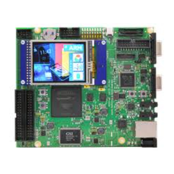
Page 35: Color Lcd Parallel Interface
These interfaces are connected to a STMicroelectronics STMPE811QTR Port Expander with Advanced Touch Screen Controller on the KEIL MCBSTM32C display board. This display board contains an Ampire AM-240320LG 2.4” Touch Panel. Schematics for this board are listed in the ARM Versatile ®... -
Page 36: Ethernet
The Soft Macro Model (SMM) self-test code includes an example code for a simple loopback operation. The Ethernet interface is supported in mbed. Related references 2.2 Running the self-test program on page 2-21. ARM 100896_0000_00_en Copyright © 2017 ARM Limited or its affiliates. All rights reserved. 3-36 Non-Confidential... -
Page 37: Vga
For example: the Left-Most Pixel (LMP) of the 0x00000400 second row is at and the LMP of the third row is at 0x41100400 0x41100800 ARM 100896_0000_00_en Copyright © 2017 ARM Limited or its affiliates. All rights reserved. 3-37 Non-Confidential... -
Page 38: Audio I 2 S
Divide ratio register (for left or right clock) [31:10] Reserved LRDIV (Left/Right). The default value is 0x80. [9:0] 12.288MHz / 48kHz / 2*(L+R) = 128. ARM 100896_0000_00_en Copyright © 2017 ARM Limited or its affiliates. All rights reserved. 3-38 Non-Confidential... - Page 39 Reserved ITCR 0x40024304 ITIP1 Integration Test Input Register 1 [31:1] Reserved SDIN 0x40024308 ITOP1 Integration Test Output Register 1 [31:4] Reserved IRQOUT LRCK SCLK SDOUT ARM 100896_0000_00_en Copyright © 2017 ARM Limited or its affiliates. All rights reserved. 3-39 Non-Confidential...
-
Page 40: Audio Configuration
The serial data is driven LOW when SDOUTEN_n is driven high, otherwise it is configured as an input pin. The audio I C control interface drives the Cirrus Logic CS42L52 codec chip on the baseboard. ARM 100896_0000_00_en Copyright © 2017 ARM Limited or its affiliates. All rights reserved. 3-40 Non-Confidential... -
Page 41: Fpga System Control And I/O
Up Counter increments when the prescale down counter reaches zero. The prescaler counter is reloaded with PRESCALE after reaching zero. 0x40028024 Reserved 0x4002804C MISC Miscellaneous control [31:7] Reserved CLCD_BL_CTRL CLCD_RD CLCD_RS CLCD_RESET Reserved SPI_nSS CLCD_CS ARM 100896_0000_00_en Copyright © 2017 ARM Limited or its affiliates. All rights reserved. 3-41 Non-Confidential... - Page 42 This chapter describes the source and derived clocks for the FPGA design. It contains the following sections: • 4.1 Source clocks on page 4-43. • 4.2 Derived clocks on page 4-44. ARM 100896_0000_00_en Copyright © 2017 ARM Limited or its affiliates. All rights reserved. 4-42 Non-Confidential...
-
Page 43: Source Clocks
5-46. CS_TCK Debugger clock Determined by the debugger. SPICFGCLK Used by MCC to load the software to the 7.5MHz ZBT memories. ARM 100896_0000_00_en Copyright © 2017 ARM Limited or its affiliates. All rights reserved. 4-43 Non-Confidential... -
Page 44: Derived Clocks
MPS2+/MB/HBI0263C/AN511 As OSCCLK[0] controls the Cortex-M3 DesignStart Eval system clock (SYSCLK), it is possible to increase the clock by changing the OSC0 value. This value can be set from 2MHz to 230MHz, with a 1% accuracy, subject to the constraints of FPGA timing performance. - Page 45 Chapter 5 Serial Communication Controller This chapter describes the Serial Communication Controller (SCC) used in the Cortex-M3 DesignStart Eval FPGA image. It contains the following sections: • 5.1 SCC interface overview on page 5-46. • 5.2 SCC memory map on page 5-47.
-
Page 46: Scc Interface Overview
Figure 5-1 SCC interface The read addresses and write addresses of the SCC interface do not use bits [1:0]. All address words are word-aligned. ARM 100896_0000_00_en Copyright © 2017 ARM Limited or its affiliates. All rights reserved. 5-46 Non-Confidential... -
Page 47: Scc Memory Map
[29:26] Reserved [25:20] Function value [19:12] Reserved [11:0] Device (value of 0/1/2 for supported clocks) 0x000000AC SYS_CFGSTAT [31:2] Reserved Error Complete 0x000000AD – Reserved 0x000000FC ARM 100896_0000_00_en Copyright © 2017 ARM Limited or its affiliates. All rights reserved. 5-47 Non-Confidential... - Page 48 Implementer ID: 0x41 = ARM [23:20] Application note IP variant number IP Architecture: 0x4 =AHB [19:16] [15:12] Reserved [11:4] Primary part number: 511 = AN511 [3:0] Reserved ARM 100896_0000_00_en Copyright © 2017 ARM Limited or its affiliates. All rights reserved. 5-48 Non-Confidential...
- Page 49 This chapter describes the steps that are required to build an FPGA bit file from the supplied source code. It contains the following sections: • 6.1 Build flow on page 6-50. • 6.2 Build requirements on page 6-52. ARM 100896_0000_00_en Copyright © 2017 ARM Limited or its affiliates. All rights reserved. 6-49 Non-Confidential...
-
Page 50: Build Flow
6.1 Build flow Build flow Cortex-M3 DesignStart Eval includes a prebuilt FPGA image file that is based on an example system. However, if your design is different from the example system, then you are required to build your own FPGA image file. - Page 51 F0FILE: an511_v1.rbe ;FPGA0 Filename Note ARM supplies an encrypted prebuilt bit file (.rbe) with the MPS2+ platform. If you are rebuilding the bit file, the file produced is not encrypted (.rbf). Therefore, if you are not using the prebuilt FPGA image and you are modifying , it is necessary to change the file extension from .rbe...
-
Page 52: Build Requirements
To build the FPGA files, use the Intel Quartus software, version 16.1 onwards. You can use the Lite Edition of Quartus Prime, which does not require a license. ARM 100896_0000_00_en Copyright © 2017 ARM Limited or its affiliates. All rights reserved. 6-52 Non-Confidential... -
Page 53: Chapter 7 Integrating With Mbed
This chapter describes the support available for integrating the FPGA system with mbed OS. It contains the following section: • 7.1 Compatibility with mbed OS on page 7-54. ™ ARM 100896_0000_00_en Copyright © 2017 ARM Limited or its affiliates. All rights reserved. 7-53 Non-Confidential... - Page 54 The MPS2+ platform is supported as a target in the mbed online compiler. https://developer.mbed.org/platforms/ARM-CM3DS/ for more information on: • Details of the platform. • Links to the example code. • mbed Cloud Quick Start application. ARM 100896_0000_00_en Copyright © 2017 ARM Limited or its affiliates. All rights reserved. 7-54 Non-Confidential...
- Page 55 Cortex-M3 DesignStart Eval. It contains the following sections: • 8.1 Performance and clocks on page 8-56. • 8.2 Utilization of default system on page 8-57. ARM 100896_0000_00_en Copyright © 2017 ARM Limited or its affiliates. All rights reserved. 8-55 Non-Confidential...
-
Page 56: Performance And Clocks
For details on the clocks used in the default system and their respective frequencies, see Table 4-2 Derived clocks on page 4-44. ARM recommends that you do not modify the clock frequencies. However, if you require modification of these clock frequencies, see 4.2 Derived clocks on page 4-44. -
Page 57: Utilization Of Default System
Table 8-1 FPGA resources Resources Value LUTs 113 560 DFFs 454 240 Memory 3.9Mbit PLLs The following table shows the Cortex-M3 DesignStart Eval code utilization of FPGA resources: Table 8-2 Resource utilization Resources Utilization LUTs DFFs Memory <1% PLLs ARM 100896_0000_00_en Copyright ©... -
Page 58: Appendix A Revisions
This appendix describes the technical changes between released issues of this book. It contains the following section: • A.1 Revisions - Cortex -M3 DesignStart Eval on page Appx-A-59. ® ™ ARM 100896_0000_00_en Copyright © 2017 ARM Limited or its affiliates. All rights reserved. Appx-A-58 Non-Confidential... -
Page 59: Revisions - Cortex -M3 Designstart Eval
Eval ® ™ This section describes the technical changes between released issues of this document. Table A-1 Issue 00 Change Location Affects First release - ARM 100896_0000_00_en Copyright © 2017 ARM Limited or its affiliates. All rights reserved. Appx-A-59 Non-Confidential...
Need help?
Do you have a question about the Cortex-M3 DesignStart and is the answer not in the manual?
Questions and answers