
Related Manuals for ARM Versatile Express Juno r2


Summary of Contents for ARM Versatile Express Juno r2
- Page 1 Versatile Express Juno r2 ® ™ Development Platform (V2M-Juno r2) Technical Reference Manual Copyright © 2015–2017 ARM Limited or its affiliates. All rights reserved. ARM 100114_0200_03_en...
- Page 2 Use of the word “partner” in reference to ARM’s customers is not intended to create or refer to any partnership relationship with any other company.
- Page 3 This document is Non-Confidential. The right to use, copy and disclose this document may be subject to license restrictions in accordance with the terms of the agreement entered into by ARM and the party that ARM delivered this document to.
-
Page 4: Table Of Contents
Resets ........................2-35 Thin Links ........................ 2-38 IOFPGA ........................2-42 HDLCD interface ....................2-45 2.10 Interrupts ........................ 2-47 2.11 USB 2.0 interface ....................2-50 ARM 100114_0200_03_en Copyright © 2015–2017 ARM Limited or its affiliates. All rights reserved. Non-Confidential... - Page 5 Secure keyboard and user push buttons connector ........Appx-A-145 A.13 ATX power connector .................. Appx-A-146 Appendix B Specifications Electrical specification ................Appx-B-148 Appendix C Revisions Revisions ....................Appx-C-150 ARM 100114_0200_03_en Copyright © 2015–2017 ARM Limited or its affiliates. All rights reserved. Non-Confidential...
- Page 6 Express Juno r2 Development Platform (V2M-Juno r2) ® ™ Technical Reference Manual. It contains the following: • About this book on page • Feedback on page ARM 100114_0200_03_en Copyright © 2015–2017 ARM Limited or its affiliates. All rights reserved. Non-Confidential...
-
Page 7: Preface
This appendix describes the technical changes between released issues of this book. Glossary The ARM Glossary is a list of terms used in ARM documentation, together with definitions for those terms. The ARM Glossary does not contain terms that are industry standard unless the ARM meaning differs from the generally accepted meaning. - Page 8 At the start or end of a signal name denotes an active-LOW signal. Additional reading This book contains information that is specific to this product. See the following documents for other relevant information. ARM 100114_0200_03_en Copyright © 2015–2017 ARM Limited or its affiliates. All rights reserved. Non-Confidential...
- Page 9 Juno ARM Development Platform SoC Technical Overview (Revision r2p0) (ARM DTO ® 0038) • AN415 Example Express 20MG design for a V2M-Juno Motherboard (ARM DAI 0415). • LogicTile Express 3MG Technical Reference Manual (ARM DUI 0449). ® • LogicTile Express 13MG Technical Reference Manual (ARM DUI 0556).
-
Page 10: Feedback
A concise explanation of your comments. ARM also welcomes general suggestions for additions and improvements. Note ARM tests the PDF only in Adobe Acrobat and Acrobat Reader, and cannot guarantee the quality of the represented document when used with any other PDF reader. ARM 100114_0200_03_en Copyright ©... - Page 11 ™ • 1.3 Location of components on the V2M-Juno r2 motherboard on page 1-15. • 1.4 Connectors on front and rear panels on page 1-16. ARM 100114_0200_03_en Copyright © 2015–2017 ARM Limited or its affiliates. All rights reserved. 1-11 Non-Confidential...
-
Page 12: Chapter 1 Introduction
Only hold the board by the edges. • Avoid touching the component pins or any other metallic element. • Do not use the board near a transmitter of electromagnetic emissions. ARM 100114_0200_03_en Copyright © 2015–2017 ARM Limited or its affiliates. All rights reserved. 1-12 Non-Confidential... -
Page 13: About The Versatile Express Juno R2 Development Platform
™ The Juno r2 Development Platform, that is, the V2M-Juno r2 motherboard, is a development motherboard that provides access to the Juno r2 ARM Development Platform SoC. This is a development chip that supports ARMv8-A software tooling, evaluation, and development. - Page 14 Debug The V2M-Juno r2 motherboard supports P-JTAG processor debug that enables connection of DSTREAM, or a compatible third-party debugger. The board also supports 32-bit trace. ARM 100114_0200_03_en Copyright © 2015–2017 ARM Limited or its affiliates. All rights reserved. 1-14 Non-Confidential...
-
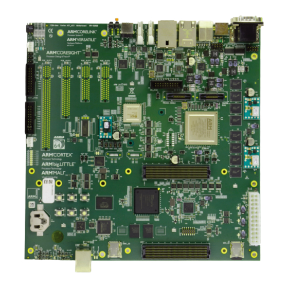
Page 15: Location Of Components On The V2M-Juno R2 Motherboard
LEDs push J2 HDRY buttons User Configuration Reserved microSD microSD card for ARM use card Ethernet only Figure 1-1 V2M-Juno r2 motherboard layout, upper face ARM 100114_0200_03_en Copyright © 2015–2017 ARM Limited or its affiliates. All rights reserved. 1-15 Non-Confidential... -
Page 16: Connectors On Front And Rear Panels
HDMI 0 Keyboard Port 2 Port 4 ON/OFF switches user push Configuration Soft Reset button connector USB 2.0 ports Figure 1-3 Rear panel ARM 100114_0200_03_en Copyright © 2015–2017 ARM Limited or its affiliates. All rights reserved. 1-16 Non-Confidential... - Page 17 2.15 Keyboard and mouse interface on page 2-56. • 2.16 Additional user key entry on page 2-57. • 2.17 Debug and trace on page 2-59. ARM 100114_0200_03_en Copyright © 2015–2017 ARM Limited or its affiliates. All rights reserved. 2-17 Non-Confidential...
-
Page 18: Overview Of V2M-Juno R2 Motherboard Hardware
The hardware infrastructure of the V2M-Juno r2 motherboard supports ARMv8-A software evaluation and tooling development using the Juno r2 SoC. The following figure shows the hardware infrastructure of the V2M-Juno r2 motherboard. ARM 100114_0200_03_en Copyright © 2015–2017 ARM Limited or its affiliates. All rights reserved. 2-18 Non-Confidential... - Page 19 V2M-Juno r2 motherboard USB 2.0 USB 2.0 USB 2.0 USB 2.0 SATA 0 SATA 1 Ethernet Figure 2-1 V2M-Juno r2 motherboard system architecture with LogicTile FPGA daughterboard ARM 100114_0200_03_en Copyright © 2015–2017 ARM Limited or its affiliates. All rights reserved. 2-19 Non-Confidential...
- Page 20 UART ports during runtime. Note The Daughterboard Configuration Controller is a microcontroller on the LogicTile that controls the configuration of the daughterboard during powerup or reset. ARM 100114_0200_03_en Copyright © 2015–2017 ARM Limited or its affiliates. All rights reserved. 2-20 Non-Confidential...
- Page 21 Denotes read or write access to the configuration microSD card through the configuration USB 2.0 port. • Debug ports: — 32-bit CoreSight Trace port. — Processor CoreSight debug (P-JTAG) port. ARM 100114_0200_03_en Copyright © 2015–2017 ARM Limited or its affiliates. All rights reserved. 2-21 Non-Confidential...
-
Page 22: Juno R2 Arm Development Platform Soc
The Juno r2 SoC development chip provides a dual-core Cortex-A72 cluster, a quad-core Cortex-A53 cluster, a quad-core Mali-T624 graphics cluster, interfaces, on-chip peripherals, and internal network connect. The following figure shows the architecture of the Juno r2 SoC. ARM 100114_0200_03_en Copyright © 2015–2017 ARM Limited or its affiliates. All rights reserved. 2-22 Non-Confidential... - Page 23 The Juno r2 SoC contains the following components and interfaces: • Dual-core Cortex-A72 cluster: — 2MB L2 cache. — NEON and Floating Point Unit (FPU). — Underdrive: Maximum operating frequency: 600MHz. ARM 100114_0200_03_en Copyright © 2015–2017 ARM Limited or its affiliates. All rights reserved. 2-23 Non-Confidential...
- Page 24 See the Juno ARM Development Platform SoC Technical Reference Manual (Revision r2p0) for more ® information. This document lists, in the Additional Reading section, references to ARM IP, such as the PL011 for example, inside the Juno r2 SoC. ARM 100114_0200_03_en Copyright ©...
-
Page 25: External Power
The mains supply powers the V2M-Juno r2 motherboard using the on-board connector, an external power supply unit, and a connector cable that ARM supplies with the V2M-Juno r2 motherboard. The external power supply unit converts mains power to 12V DC and this connects to the 12V DC connector on the rear panel of the case. -
Page 26: Power Management And Temperature Protection
Varying the Juno r2 SoC PLL dividers during runtime supports frequency scaling. Note ARM recommends that you use this method to achieve frequency scaling and do not use external control of the clock generators through the V2M-Juno r2 motherboard SCP I C interface. - Page 27 It also selectively powers down parts of the chip when it exceeds the temperature budget. The PVT sensor is calibrated during board manufacture. ARM 100114_0200_03_en Copyright © 2015–2017 ARM Limited or its affiliates. All rights reserved. 2-27 Non-Confidential...
-
Page 28: Clocks
You can change the operational clock frequencies by modifying the configuration file. board.txt Note ARM recommends that you operate the V2M-Juno r2 motherboard at the default clock frequencies. Related concepts 3.3.3 Contents of the directory on page 3-72. 2.5.2 Juno r2 SoC and V2M-Juno r2 motherboard clocks The following figure shows the Juno r2 SoC clocks and clock domains. - Page 29 Versatile Express LogicTile daughterboard Figure 2-4 Juno r2 SoC system clocks The following table shows the internal Juno r2 SoC and V2M-Juno r2 motherboard clocks and their sources. ARM 100114_0200_03_en Copyright © 2015–2017 ARM Limited or its affiliates. All rights reserved. 2-29 Non-Confidential...
- Page 30 C clock generator and reference clock for the SCP PLL inside the Juno r2 SoC. This derives the following clock: SCPHCLK: SCP subsystem and AHB expansion area clock. ARM 100114_0200_03_en Copyright © 2015–2017 ARM Limited or its affiliates. All rights reserved. 2-30 Non-Confidential...
- Page 31 Clock in the transmit direction from the TLX-400 AXI master interface Thin Links AXI master interface on the Juno r2 reference clock SoC. generator in Juno r2 ARM 100114_0200_03_en Copyright © 2015–2017 ARM Limited or its affiliates. All rights reserved. 2-31 Non-Confidential...
- Page 32 The Juno r2 SoC has internal PLLs and clock generators that generate clocks to drive the Juno r2 SoC internal systems. 2.5.3 IOFPGA clocks The following figure shows the IOFPFA clocks and clock domains. ARM 100114_0200_03_en Copyright © 2015–2017 ARM Limited or its affiliates. All rights reserved. 2-32 Non-Confidential...
- Page 33 OSCCLK 9 on the V2M-Juno r2 motherboard. The clock source then switches to SMB_CLKO from the Juno r2 SoC that becomes the master clock for the SMB_CLK domain during runtime. ARM 100114_0200_03_en Copyright © 2015–2017 ARM Limited or its affiliates. All rights reserved. 2-33 Non-Confidential...
- Page 34 The frequency of the clock 32kHz is 32.768kHz. SMB_MCLK MCC 50MHz Master clock for the SMB_MCLK domain that includes the MCC, and the MCC to AHB fabric, in the IOFPGA. ARM 100114_0200_03_en Copyright © 2015–2017 ARM Limited or its affiliates. All rights reserved. 2-34 Non-Confidential...
-
Page 35: Resets
1.4 Connectors on front and rear panels on page 1-16. 2.6.2 Reset architecture The following figure shows an overview of the V2M-Juno r2 motherboard reset system. ARM 100114_0200_03_en Copyright © 2015–2017 ARM Limited or its affiliates. All rights reserved. 2-35 Non-Confidential... - Page 36 Figure 2-6 V2M-Juno r2 motherboard resets CB_nPOR This is the main powerup reset for the Juno r2 ARM Development Platform SoC, and the devices and peripherals on the V2M-Juno r2 motherboard including the IOFPGA. The CB_nPOR signal drives the nPORESET signal inside the Juno r2 SoC.
- Page 37 Hard Reset ON/OFF Soft Reset ATXON CB_CFGnRST CB_VRAMP IOFPGA_nRST CFG_nRST CB_nPOR (nPORESET) CB_nRST CB_nTRST Figure 2-7 V2M-Juno r2 motherboard reset and configuration timing cycle ARM 100114_0200_03_en Copyright © 2015–2017 ARM Limited or its affiliates. All rights reserved. 2-37 Non-Confidential...
-
Page 38: Thin Links
— Forward direction, that is, from the FPGA to the Juno r2 SoC: 246MBps. — Reverse direction, that is, from the Juno r2 SoC to the FPGA: 305MBps. Note ARM recommends that you operate the Thin Links interfaces at the default speeds. See 3.3.4 Contents of directory on page 3-73... - Page 39 2 Hardware Description 2.7 Thin Links Note Any Versatile Express LogicTile daughterboard fitted in the tile site that implements an ARM application note meets these timing requirements. Any design that you implement in a Versatile Express LogicTile daughterboard, or in your own daughterboard, must meet these timing requirements.
- Page 40 The Thin Links non-coherent AXI slave interface uses one fewer control bit than the ACE interface in each direction, and one more data bit than the ACE interface in each direction. ARM 100114_0200_03_en Copyright © 2015–2017 ARM Limited or its affiliates. All rights reserved. 2-40 Non-Confidential...
- Page 41 The Thin Links ACE slave interface uses one more control bit than the non-coherent, AXI interface in each direction, and one fewer data bit than the non-coherent, AXI interface in each direction. ARM 100114_0200_03_en Copyright © 2015–2017 ARM Limited or its affiliates. All rights reserved. 2-41 Non-Confidential...
-
Page 42: Iofpga
The following figure shows the internal architecture of the IOFPGA and its connectivity to external peripherals, including the external interrupts to the GIC-400 interrupt controller in the Juno r2 SoC. ARM 100114_0200_03_en Copyright © 2015–2017 ARM Limited or its affiliates. All rights reserved. 2-42 Non-Confidential... - Page 43 User push PLO61 (0) buttons SP804 (2/3) PLO61 (1) Not used SB_IRQ[11] SB_IRQ[6] HDRY HDRY Versatile Express LogicTile daughteraboard FPGA Figure 2-11 IOFPGA internal architecture ARM 100114_0200_03_en Copyright © 2015–2017 ARM Limited or its affiliates. All rights reserved. 2-43 Non-Confidential...
- Page 44 AMBA 3 APB Protocol Specification v1.0. Note The peripheral versions apply to the Revision B V2M-Juno r2 motherboard. Related concepts 4.2.2 IOFPGA system peripherals memory map on page 4-85. ARM 100114_0200_03_en Copyright © 2015–2017 ARM Limited or its affiliates. All rights reserved. 2-44 Non-Confidential...
-
Page 45: Hdlcd Interface
The same audio stream connects to both HDMI connectors. Note Software that ARM supplies with the V2M-Juno r2 motherboard configures the Juno r2 SoC and board to enable correct operation of the HDLCD interface and correct HDMI output. The following figure shows the HDLCD video system on the V2M-Juno r2 motherboard. - Page 46 1.3 Location of components on the V2M-Juno r2 motherboard on page 1-15. 1.4 Connectors on front and rear panels on page 1-16. A.8 HDMI connectors on page Appx-A-132. ARM 100114_0200_03_en Copyright © 2015–2017 ARM Limited or its affiliates. All rights reserved. 2-46 Non-Confidential...
-
Page 47: Interrupts
The following figure shows an overview of the external interrupt signals from the V2M-Juno r2 motherboard peripherals to the GIC-400 interrupt controller in the Juno r2 SoC. ARM 100114_0200_03_en Copyright © 2015–2017 ARM Limited or its affiliates. All rights reserved. 2-47 Non-Confidential... - Page 48 Table 2-5 External interrupt signals to Juno r2 SoC Interrupt ID GIC IRQ ID Motherboard signal Source name 96-99 64-67 Juno r2 SoC internal peripherals and systems. SB_IRQ[0] IOFPGA-PL031 RTC. ARM 100114_0200_03_en Copyright © 2015–2017 ARM Limited or its affiliates. All rights reserved. 2-48 Non-Confidential...
- Page 49 See the Juno ARM Development Platform SoC Technical Reference Manual (Revision r2p0) for ® information on the interrupts from the systems in the Juno r2 SoC. ARM 100114_0200_03_en Copyright © 2015–2017 ARM Limited or its affiliates. All rights reserved. 2-49 Non-Confidential...
-
Page 50: Usb 2.0 Interface
1.4 Connectors on front and rear panels on page 1-16. A.2 Configuration 10Mbps Ethernet and dual-USB connector on page Appx-A-126. A.3 PCI Express Gigabit Ethernet and dual-USB connector on page Appx-A-127. ARM 100114_0200_03_en Copyright © 2015–2017 ARM Limited or its affiliates. All rights reserved. 2-50 Non-Confidential... -
Page 51: Smc 10/100 Ethernet Interface
1.3 Location of components on the V2M-Juno r2 motherboard on page 1-15. 1.4 Connectors on front and rear panels on page 1-16. A.4 SMC 10/100 Ethernet connector on page Appx-A-128. ARM 100114_0200_03_en Copyright © 2015–2017 ARM Limited or its affiliates. All rights reserved. 2-51 Non-Confidential... -
Page 52: Uart Interface
Juno r2 SoC UART 1 interface. The following figure shows the UART interface to the V2M-Juno r2 motherboard. ARM 100114_0200_03_en Copyright © 2015–2017 ARM Limited or its affiliates. All rights reserved. 2-52 Non-Confidential... - Page 53 1.3 Location of components on the V2M-Juno r2 motherboard on page 1-15. 1.4 Connectors on front and rear panels on page 1-16. A.11 Dual-UART connector on page Appx-A-143. ARM 100114_0200_03_en Copyright © 2015–2017 ARM Limited or its affiliates. All rights reserved. 2-53 Non-Confidential...
-
Page 54: Pci Express System
The following table shows the four PCIe expansion slots on the V2M-Juno r2 motherboard. Table 2-6 PCI Express expansion slots Slot number Connector size-PCIe lanes Used lanes Unused lanes Slot 0 ×4 Slot 1 ×4 ARM 100114_0200_03_en Copyright © 2015–2017 ARM Limited or its affiliates. All rights reserved. 2-54 Non-Confidential... - Page 55 1.3 Location of components on the V2M-Juno r2 motherboard on page 1-15. 1.4 Connectors on front and rear panels on page 1-16. A.3 PCI Express Gigabit Ethernet and dual-USB connector on page Appx-A-127. ARM 100114_0200_03_en Copyright © 2015–2017 ARM Limited or its affiliates. All rights reserved. 2-55 Non-Confidential...
-
Page 56: Keyboard And Mouse Interface
1.3 Location of components on the V2M-Juno r2 motherboard on page 1-15. 1.4 Connectors on front and rear panels on page 1-16. A.7 Keyboard and Mouse Interface (KMI) connector on page Appx-A-131. ARM 100114_0200_03_en Copyright © 2015–2017 ARM Limited or its affiliates. All rights reserved. 2-56 Non-Confidential... -
Page 57: Additional User Key Entry
Figure 2-19 Additional user key entry interface The following figure shows an example trusted keyboard design using an external custom device that connects to the secure keyboard entry port. ARM 100114_0200_03_en Copyright © 2015–2017 ARM Limited or its affiliates. All rights reserved. 2-57 Non-Confidential... - Page 58 1.3 Location of components on the V2M-Juno r2 motherboard on page 1-15. 1.4 Connectors on front and rear panels on page 1-16. A.12 Secure keyboard and user push buttons connector on page Appx-A-145. ARM 100114_0200_03_en Copyright © 2015–2017 ARM Limited or its affiliates. All rights reserved. 2-58 Non-Confidential...
-
Page 59: Debug And Trace
TRACEA-SINGLE connector to run 16-bit trace or to both the TRACEA-SINGLE and TRACEB-DUAL connector to run 32-bit trace. The following figure shows an overview of the V2M-Juno r2 motherboard debug and trace architecture. ARM 100114_0200_03_en Copyright © 2015–2017 ARM Limited or its affiliates. All rights reserved. 2-59 Non-Confidential... - Page 60 Figure 2-21 V2M-Juno r2 motherboard debug architecture See the Juno ARM Development Platform SoC Technical Reference Manual (Revision r2p0) for more ® information on the Juno r2 SoC debug architecture. ARM 100114_0200_03_en Copyright © 2015–2017 ARM Limited or its affiliates. All rights reserved. 2-60 Non-Confidential...
- Page 61 1.3 Location of components on the V2M-Juno r2 motherboard on page 1-15. 1.4 Connectors on front and rear panels on page 1-16. A.1.1 P-JTAG connector on page Appx-A-122. A.1.2 Trace connectors on page Appx-A-123. ARM 100114_0200_03_en Copyright © 2015–2017 ARM Limited or its affiliates. All rights reserved. 2-61 Non-Confidential...
-
Page 62: Configuration
3-70. • 3.4 Configuration switches on page 3-75. • 3.5 Use of reset push buttons on page 3-77. • 3.6 Command-line interface on page 3-78. ARM 100114_0200_03_en Copyright © 2015–2017 ARM Limited or its affiliates. All rights reserved. 3-62 Non-Confidential... -
Page 63: Overview Of The V2M-Juno R2 Motherboard Configuration System
Hardware RESET or ON/OFF/Soft Reset button pressed? Hardware RESET button pressed or ON/OFF/ Soft Reset button pressed for more than two seconds Figure 3-1 V2M-Juno r2 motherboard configuration system ARM 100114_0200_03_en Copyright © 2015–2017 ARM Limited or its affiliates. All rights reserved. 3-63 Non-Confidential... - Page 64 If the MCC does not find a configuration directory that matches the HBI number of the board, the configuration process fails and the board enters the standby-state. ARM 100114_0200_03_en Copyright © 2015–2017 ARM Limited or its affiliates. All rights reserved. 3-64 Non-Confidential...
-
Page 65: Configuration Process And Operating Modes
The following figure shows the configuration process and the transitions between the standby-state, operating-state, and sleep-state of the V2M-Juno r2 motherboard. ARM 100114_0200_03_en Copyright © 2015–2017 ARM Limited or its affiliates. All rights reserved. 3-65 Non-Confidential... - Page 66 LogicTile daughterboard and reads them to determine the HBI identification codes for the boards. 3. The system enters the standby-state. 4. The system enables the MCC command-line interface on the UART. ARM 100114_0200_03_en Copyright © 2015–2017 ARM Limited or its affiliates. All rights reserved. 3-66 Non-Confidential...
- Page 67 The powerdown sequence takes the V2M-Juno r2 motherboard from the operating-state to the standby-state. The powerdown sequence is as follows: 1. The powerdown sequence begins with one of the following: ARM 100114_0200_03_en Copyright © 2015–2017 ARM Limited or its affiliates. All rights reserved. 3-67 Non-Confidential...
- Page 68 The wake-up sequence takes the Juno r2 SoC from the sleep-state to the operating-state. Application software resumes operation from the previous operating point with all data restored. ARM 100114_0200_03_en Copyright © 2015–2017 ARM Limited or its affiliates. All rights reserved. 3-68 Non-Confidential...
- Page 69 5. The SCP releases the Power Policy Unit (PPU) to start the application cluster boot sequence. 6. The application code resumes from the point when the Juno r2 SoC went into the sleep-state. ARM 100114_0200_03_en Copyright © 2015–2017 ARM Limited or its affiliates. All rights reserved. 3-69 Non-Confidential...
-
Page 70: Configuration Files
File names that you generate must be in lower case. • Directory names must be in upper case. • All configuration files must end in DOS line endings, 0x0D 0x0A ARM 100114_0200_03_en Copyright © 2015–2017 ARM Limited or its affiliates. All rights reserved. 3-70 Non-Confidential... - Page 71 Contains application files that the MCC can load into SRAM or NOR flash. The section IMAGES in the file defines the file that the MCC loads. config.txt ARM 100114_0200_03_en Copyright © 2015–2017 ARM Limited or its affiliates. All rights reserved. 3-71 Non-Confidential...
- Page 72 A file of the form . MCC BIOS image that the file defines. mbb_vxxx.ebf board.txt A file of the form IOFPGA image file. io_bxxx.bit ARM 100114_0200_03_en Copyright © 2015–2017 ARM Limited or its affiliates. All rights reserved. 3-72 Non-Confidential...
- Page 73 ;A53 PLL Register 0 (700MHz) SCC: 0x10C 0x0000D100 ;A53 PLL Register 1 SCC: 0x0F8 0x0BEC0000 ;BL1 entry point Caution ARM reserves these registers. You must not write to them. ARM 100114_0200_03_en Copyright © 2015–2017 ARM Limited or its affiliates. All rights reserved. 3-73 Non-Confidential...
- Page 74 • ARM AP Boot ROM. bl1.bin • Firmware Image Package that contains subsequent firmware images. fip.bin • Linux kernel. Image • Juno device tree. juno.dtb ARM 100114_0200_03_en Copyright © 2015–2017 ARM Limited or its affiliates. All rights reserved. 3-74 Non-Confidential...
-
Page 75: Configuration Switches
An external controller can toggle UART0 SER0_DSR, pin 6, HIGH for 100ms to put the V2M-Juno r2 motherboard into standby-state. This is equivalent to pressing the Hardware Reset button. Power cycling the board also places the system in standby-state. ARM 100114_0200_03_en Copyright © 2015–2017 ARM Limited or its affiliates. All rights reserved. 3-75 Non-Confidential... - Page 76 Set UART0 SER0_CTS, pin 8, LOW to select system mode, or set it HIGH to select MCC mode. Remote UART0 control requires a full null modem cable that ARM supplies with the V2M-Juno r2 motherboard. The following figure shows the cable wiring.
-
Page 77: Use Of Reset Push Buttons
2.6.1 Reset push buttons on page 2-35. Related references 1.3 Location of components on the V2M-Juno r2 motherboard on page 1-15. 1.4 Connectors on front and rear panels on page 1-16. ARM 100114_0200_03_en Copyright © 2015–2017 ARM Limited or its affiliates. All rights reserved. 3-77 Non-Confidential... -
Page 78: Command-Line Interface
Change to the debug menu. DEL filename Delete file filename. DIR [mask] Display a list of files in the directory. EEPROM Change to the EEPROM menu. ARM 100114_0200_03_en Copyright © 2015–2017 ARM Limited or its affiliates. All rights reserved. 3-78 Non-Confidential... - Page 79 EEPROM submenu. The contents of the V2M-Juno r2 EEPROM motherboard EEPROMs identify the specific board variant and might contain data to load to the other devices on the board. ARM 100114_0200_03_en Copyright © 2015–2017 ARM Limited or its affiliates. All rights reserved. 3-79 Non-Confidential...
- Page 80 Display this help. READIMAGES Read images stored in Motherboard EEPROM. READCF [0] Read configuration EEPROM. READRANGE [0] [start] [end] Read EEPROM between start and end. ARM 100114_0200_03_en Copyright © 2015–2017 ARM Limited or its affiliates. All rights reserved. 3-80 Non-Confidential...
- Page 81 4.3 APB system registers on page 4-89. • 4.4 APB system configuration registers on page 4-103. • 4.5 APB energy meter registers on page 4-107. ARM 100114_0200_03_en Copyright © 2015–2017 ARM Limited or its affiliates. All rights reserved. 4-81 Non-Confidential...
-
Page 82: About This Programmers Model
4.4.1 APB system configuration register summary on page 4-103, and 4.5.1 APB energy register summary on page 4-107 describe register access type as follows: Read and write. Read-only. Write-only. ARM 100114_0200_03_en Copyright © 2015–2017 ARM Limited or its affiliates. All rights reserved. 4-82 Non-Confidential... -
Page 83: V2M-Juno R2 Motherboard Memory Maps
V2M-Juno r2 motherboard. The security status is exported security. Chip select CS3 inside the SMC accesses the low-bandwidth system peripherals inside the IOFPGA and is at 0x001C000000 ARM 100114_0200_03_en Copyright © 2015–2017 ARM Limited or its affiliates. All rights reserved. 4-83 Non-Confidential... - Page 84 Description 0x08000000-0x0BFFFFFF 64MB CS0-Motherboard NOR flash. 0x0C000000-0x13FFFFFF 128MB Reserved. Do not write to or read from these addresses. 0x14000000-0x1403FFFF 256KB CS1-256KB internal IOFPGA block RAM. ARM 100114_0200_03_en Copyright © 2015–2017 ARM Limited or its affiliates. All rights reserved. 4-84 Non-Confidential...
- Page 85 IOFPGA that the Juno r2 SoC does not provide. The following figure shows the mapping of the IOFPGA system peripherals memory map into the SMC memory map. ARM 100114_0200_03_en Copyright © 2015–2017 ARM Limited or its affiliates. All rights reserved. 4-85 Non-Confidential...
- Page 86 0x001C000000 IOFPGA peripherals memory map Figure 4-2 V2M-Juno r2 motherboard IOFPGA system peripherals memory map The following table shows the IOFPGA system peripherals memory map. ARM 100114_0200_03_en Copyright © 2015–2017 ARM Limited or its affiliates. All rights reserved. 4-86 Non-Confidential...
- Page 87 . The security is programmable access security. 0x0080000000 0x0880000000 The following figure shows the mapping of the DDR3L memory map into the Juno r2 SoC top-level application memory map. ARM 100114_0200_03_en Copyright © 2015–2017 ARM Limited or its affiliates. All rights reserved. 4-87 Non-Confidential...
- Page 88 See the Juno ARM Development Platform SoC Technical Reference Manual (Revision r2p0) for ® information on other areas of the top-level memory map of the Juno r2 SoC. ARM 100114_0200_03_en Copyright © 2015–2017 ARM Limited or its affiliates. All rights reserved. 4-88 Non-Confidential...
-
Page 89: Apb System Registers
4.3.12 SYS_PROC_ID0 Register on page 4-97. 0x0088 SYS_PROC_ID1 0x0X000XXX 32 4.3.13 SYS_PROC_ID1 Register on page 4-98. 0x0120 SYS_FAN_SPEED 0x00000000 32 4.3.14 SYS_FAN_SPEED Register on page 4-99. ARM 100114_0200_03_en Copyright © 2015–2017 ARM Limited or its affiliates. All rights reserved. 4-89 Non-Confidential... - Page 90 0x3 Rev D board. This board contains the Juno r2 SoC. [26:16] HBI board number in BCD: HBI0262. 0x262 [15:12] Build Build variant of board: All builds. ARM 100114_0200_03_en Copyright © 2015–2017 ARM Limited or its affiliates. All rights reserved. 4-90 Non-Confidential...
- Page 91 Indicates the value of the physical configuration switch SW[1]: [30] SW[0] Indicates the value of the physical configuration switch SW[0]: [29] nUART0CTS UART0 CTS signal. [28] nUART0DSR UART0 DSR signal. ARM 100114_0200_03_en Copyright © 2015–2017 ARM Limited or its affiliates. All rights reserved. 4-91 Non-Confidential...
- Page 92 Set or read the user LED states: OFF. Related concepts 4.3.1 APB system register summary on page 4-89. 4.3.5 SYS_100HZ Register The SYS_100HZ Register characteristics are: ARM 100114_0200_03_en Copyright © 2015–2017 ARM Limited or its affiliates. All rights reserved. 4-92 Non-Confidential...
- Page 93 You use the SYS_FLAGSCLR Register to clear bits in the SYS_FLAGS Register. Write clear the associated flag. Write to leave the associated flag unchanged. ARM 100114_0200_03_en Copyright © 2015–2017 ARM Limited or its affiliates. All rights reserved. 4-93 Non-Confidential...
- Page 94 Note The configuration system does not use the contents of this register for board configuration. Related concepts 4.3.1 APB system register summary on page 4-89. ARM 100114_0200_03_en Copyright © 2015–2017 ARM Limited or its affiliates. All rights reserved. 4-94 Non-Confidential...
- Page 95 The following figure shows the bit assignments. 20 19 14 13 12 Reserved Reserved Reserved SWINT nDBDET Figure 4-10 SYS_MISC Register bit assignments The following table shows the bit assignments. ARM 100114_0200_03_en Copyright © 2015–2017 ARM Limited or its affiliates. All rights reserved. 4-95 Non-Confidential...
- Page 96 Available in all V2M-Juno r2 motherboard configurations. The following figure shows the bit assignments. Reserved PCIE_RSTHALT PCIE_nPERST Figure 4-11 SYS_PCIE_CNTL Register bit assignments The following table shows the bit assignments. ARM 100114_0200_03_en Copyright © 2015–2017 ARM Limited or its affiliates. All rights reserved. 4-96 Non-Confidential...
- Page 97 4.3.12 SYS_PROC_ID0 Register The SYS_PROC_ID0 Register characteristics are: Purpose Identifies the active clusters in the Juno r2 SoC. Usage constraints There are no usage constraints. ARM 100114_0200_03_en Copyright © 2015–2017 ARM Limited or its affiliates. All rights reserved. 4-97 Non-Confidential...
- Page 98 16 15 12 11 BOARD BOARD PROC_ID1 Reserved HBI BOARD NUMBER REVISION VARIANT Figure 4-14 SYS_PROC_ID1 Register bit assignments The following table shows the bit assignments. ARM 100114_0200_03_en Copyright © 2015–2017 ARM Limited or its affiliates. All rights reserved. 4-98 Non-Confidential...
- Page 99 Available in all V2M-Juno r2 motherboard configurations. The following figure shows the bit assignments. FAN_SPEED Reserved UPDATE_FAN_SPEED Figure 4-15 SYS_FAN_SPEED Register bit assignments The following table shows the bit assignments. ARM 100114_0200_03_en Copyright © 2015–2017 ARM Limited or its affiliates. All rights reserved. 4-99 Non-Confidential...
- Page 100 21 20 19 18 17 16 15 14 Reserved Reserved TimerEn3Sel TimerEn0Sel Reserved Reserved TimerEn2Sel TimerEn1Sel Reserved Figure 4-16 SP810_CTRL Register bit assignments The following table shows the bit assignments. ARM 100114_0200_03_en Copyright © 2015–2017 ARM Limited or its affiliates. All rights reserved. 4-100 Non-Confidential...
- Page 101 Reserved. If you write to this register, you must write all zeros to these bits. If you read this register, you must ignore these bits. ARM 100114_0200_03_en Copyright © 2015–2017 ARM Limited or its affiliates. All rights reserved. 4-101 Non-Confidential...
- Page 102 If you read this register, you must ignore these bits. Related concepts 4.3.1 APB system register summary on page 4-89. ARM 100114_0200_03_en Copyright © 2015–2017 ARM Limited or its affiliates. All rights reserved. 4-102 Non-Confidential...
-
Page 103: Apb System Configuration Registers
Figure 4-17 SYS_CFGDATA_OUT Register bit assignments The following table shows the bit assignments. Table 4-20 SYS_CFGDATA_OUT Register bit assignments Bits Name Function [31:0] SYS_CFGDATA Write-data or read-data. ARM 100114_0200_03_en Copyright © 2015–2017 ARM Limited or its affiliates. All rights reserved. 4-103 Non-Confidential... - Page 104 Reserved. If you write to this register, you must write all zeros to these bits. If you read this register, you must ignore these bits. ARM 100114_0200_03_en Copyright © 2015–2017 ARM Limited or its affiliates. All rights reserved. 4-104 Non-Confidential...
- Page 105 The following figure shows the bit assignments. Reserved Configuration error Configuration complete Figure 4-19 SYS_CFGSTAT Register bit assignments The following table shows the bit assignments. ARM 100114_0200_03_en Copyright © 2015–2017 ARM Limited or its affiliates. All rights reserved. 4-105 Non-Confidential...
- Page 106 Configuration A write to SYS_CFGCTRL clears this bit: complete Configuration not complete. Configuration complete. Related concepts 4.4.1 APB system configuration register summary on page 4-103. ARM 100114_0200_03_en Copyright © 2015–2017 ARM Limited or its affiliates. All rights reserved. 4-106 Non-Confidential...
-
Page 107: Apb Energy Meter Registers
Therefore you can use a Cortex-A72 core to measure the cumulative energy consumption of the Cortex-A72 cluster and a Cortex-A53 core to read the cumulative energy consumption of the Cortex-A53 cluster. ARM 100114_0200_03_en Copyright © 2015–2017 ARM Limited or its affiliates. All rights reserved. 4-107 Non-Confidential... - Page 108 4-119. 0x011C 0x00000000 SYS_ENM_H_GPU 4.5.17 SYS_ENM_GPU Register on page 4-119. Related concepts 2.4.1 Power control and Dynamic Voltage and Frequency Scaling (DVFS) on page 2-26. ARM 100114_0200_03_en Copyright © 2015–2017 ARM Limited or its affiliates. All rights reserved. 4-108 Non-Confidential...
- Page 109 Available in all V2M-Juno r2 motherboard configurations. The following figure shows the bit assignments. Reserved SYS_I_A72 Figure 4-21 SYS_I_A72 Register bit assignments The following table shows the bit assignments. ARM 100114_0200_03_en Copyright © 2015–2017 ARM Limited or its affiliates. All rights reserved. 4-109 Non-Confidential...
- Page 110 The SYS_I_GPU Register characteristics are: Purpose Contains a 12-bit representation of the instantaneous current consumption of the Mali-T624 GPU cluster. Usage constraints This register is read-only. ARM 100114_0200_03_en Copyright © 2015–2017 ARM Limited or its affiliates. All rights reserved. 4-110 Non-Confidential...
- Page 111 • Measured voltage = (SYS_V_SYS+1)/1622 volts. • The CB_nRST reset signal resets the register to zero. The register then updates every 100µs after the reset. ARM 100114_0200_03_en Copyright © 2015–2017 ARM Limited or its affiliates. All rights reserved. 4-111 Non-Confidential...
- Page 112 Available in all V2M-Juno r2 motherboard configurations. The following figure shows the bit assignments. Reserved SYS_V_A53 Figure 4-26 SYS_V_A53 Register bit assignments The following table shows the bit assignments. ARM 100114_0200_03_en Copyright © 2015–2017 ARM Limited or its affiliates. All rights reserved. 4-112 Non-Confidential...
- Page 113 SYS_POW_SYS Register The SYS_POW_SYS Register characteristics are: Purpose Contains a 24-bit representation of the instantaneous power consumption of the Juno r2 SoC outside the clusters. ARM 100114_0200_03_en Copyright © 2015–2017 ARM Limited or its affiliates. All rights reserved. 4-113 Non-Confidential...
- Page 114 Available in all V2M-Juno r2 motherboard configurations. The following figure shows the bit assignments. Reserved SYS_POW_A72 Figure 4-29 SYS_POW_A72 Register bit assignments The following table shows the bit assignments. ARM 100114_0200_03_en Copyright © 2015–2017 ARM Limited or its affiliates. All rights reserved. 4-114 Non-Confidential...
- Page 115 4.5.1 APB energy register summary on page 4-107. 4.5.13 SYS_POW_GPU Register The SYS_POW_GPU Register characteristics are: Purpose Contains a 24-bit representation of the instantaneous power consumption of the Mali-T624 GPU cluster. ARM 100114_0200_03_en Copyright © 2015–2017 ARM Limited or its affiliates. All rights reserved. 4-115 Non-Confidential...
- Page 116 Available in all V2M-Juno r2 motherboard configurations. The following figure shows the bit assignments. SYS_ENM_H_SYS SYS_ENM_L_SYS Figure 4-32 SYS_ENM_SYS Register bit assignments The following table shows the bit assignments. ARM 100114_0200_03_en Copyright © 2015–2017 ARM Limited or its affiliates. All rights reserved. 4-116 Non-Confidential...
- Page 117 Available in all V2M-Juno r2 motherboard configurations. The following figure shows the bit assignments. SYS_ENM_H_A72 SYS_ENM_L_A72 Figure 4-33 SYS_ENM_A72 Register bit assignments The following table shows the bit assignments. ARM 100114_0200_03_en Copyright © 2015–2017 ARM Limited or its affiliates. All rights reserved. 4-117 Non-Confidential...
- Page 118 Available in all V2M-Juno r2 motherboard configurations. The following figure shows the bit assignments. 32 31 SYS_ENM_H_A53 SYS_ENM_L_A53 Figure 4-34 SYS_ENM_A53 Register bit assignments The following table shows the bit assignments. ARM 100114_0200_03_en Copyright © 2015–2017 ARM Limited or its affiliates. All rights reserved. 4-118 Non-Confidential...
- Page 119 Available in all V2M-Juno r2 motherboard configurations. The following figure shows the bit assignments. SYS_ENM_H_GPU SYS_ENM_L_GPU Figure 4-35 SYS_ENM_GPU Register bit assignments The following table shows the bit assignments. ARM 100114_0200_03_en Copyright © 2015–2017 ARM Limited or its affiliates. All rights reserved. 4-119 Non-Confidential...
- Page 120 The CB_nRST reset signal resets the register to zero. The register then updates every 100µs after the reset. Related concepts 4.5.1 APB energy register summary on page 4-107. ARM 100114_0200_03_en Copyright © 2015–2017 ARM Limited or its affiliates. All rights reserved. 4-120 Non-Confidential...
-
Page 121: Appendix A Signal Descriptions
A.11 Dual-UART connector on page Appx-A-143. • A.12 Secure keyboard and user push buttons connector on page Appx-A-145. • A.13 ATX power connector on page Appx-A-146. ARM 100114_0200_03_en Copyright © 2015–2017 ARM Limited or its affiliates. All rights reserved. Appx-A-121 Non-Confidential... -
Page 122: Debug Connectors
Pins 7 and 9 are dual-mode pins that enable the Juno r2 SoC to support both the JTAG and SWD protocols. Related concepts 2.17 Debug and trace on page 2-59. ARM 100114_0200_03_en Copyright © 2015–2017 ARM Limited or its affiliates. All rights reserved. Appx-A-122 Non-Confidential... - Page 123 No connection TRACE_CLKA EDBGRQ DBGACK No connection/nSRST 10 TDO/SWO 1V8 reference RTCK 1V8_OUT TCK/SWCLK TRACEDATA[7] TMS/SWDIO TRACEDATA[6] TRACEDATA[5] nTRST TRACEDATA[4] TRACEDATA[15] TRACEDATA[3] TRACEDATA[14] TRACEDATA[2] TRACEDATA[13] TRACEDATA[1] ARM 100114_0200_03_en Copyright © 2015–2017 ARM Limited or its affiliates. All rights reserved. Appx-A-123 Non-Confidential...
- Page 124 TRACEDATA[17] TRACEDATA[28] 30 TRACEDATA[27] 32 TRACEDATA[26] 34 1V8 reference TRACEDATA[25] 36 No connection TRACEDATA[24] 38 TRACEDATA[16] Related concepts 2.17 Debug and trace on page 2-59. ARM 100114_0200_03_en Copyright © 2015–2017 ARM Limited or its affiliates. All rights reserved. Appx-A-124 Non-Confidential...
- Page 125 A Signal Descriptions A.1 Debug connectors Related references 1.3 Location of components on the V2M-Juno r2 motherboard on page 1-15. ARM 100114_0200_03_en Copyright © 2015–2017 ARM Limited or its affiliates. All rights reserved. Appx-A-125 Non-Confidential...
-
Page 126: Configuration 10Mbps Ethernet And Dual-Usb Connector
3.3.1 Overview of configuration files and microSD card directory structure on page 3-70. Related references 1.3 Location of components on the V2M-Juno r2 motherboard on page 1-15. 1.4 Connectors on front and rear panels on page 1-16. ARM 100114_0200_03_en Copyright © 2015–2017 ARM Limited or its affiliates. All rights reserved. Appx-A-126 Non-Confidential... -
Page 127: Pci Express Gigabit Ethernet And Dual-Usb Connector
2.14.4 Gigabit Ethernet port on page 2-55. Related references 1.3 Location of components on the V2M-Juno r2 motherboard on page 1-15. 1.4 Connectors on front and rear panels on page 1-16. ARM 100114_0200_03_en Copyright © 2015–2017 ARM Limited or its affiliates. All rights reserved. Appx-A-127 Non-Confidential... -
Page 128: Smc 10/100 Ethernet Connector
2.12 SMC 10/100 Ethernet interface on page 2-51. Related references 1.3 Location of components on the V2M-Juno r2 motherboard on page 1-15. 1.4 Connectors on front and rear panels on page 1-16. ARM 100114_0200_03_en Copyright © 2015–2017 ARM Limited or its affiliates. All rights reserved. Appx-A-128 Non-Confidential... -
Page 129: Configuration Usb Connector
3.3.1 Overview of configuration files and microSD card directory structure on page 3-70. Related references 1.3 Location of components on the V2M-Juno r2 motherboard on page 1-15. 1.4 Connectors on front and rear panels on page 1-16. ARM 100114_0200_03_en Copyright © 2015–2017 ARM Limited or its affiliates. All rights reserved. Appx-A-129 Non-Confidential... -
Page 130: Header Connectors
The constraints file, an415_wrapper.xdc, available in AN415 Example Express 20MG design for a V2M-Juno Motherboard, lists the header signals. Related references 1.3 Location of components on the V2M-Juno r2 motherboard on page 1-15. ARM 100114_0200_03_en Copyright © 2015–2017 ARM Limited or its affiliates. All rights reserved. Appx-A-130 Non-Confidential... -
Page 131: Keyboard And Mouse Interface (Kmi) Connector
2.15 Keyboard and mouse interface on page 2-56. Related references 1.3 Location of components on the V2M-Juno r2 motherboard on page 1-15. 1.4 Connectors on front and rear panels on page 1-16. ARM 100114_0200_03_en Copyright © 2015–2017 ARM Limited or its affiliates. All rights reserved. Appx-A-131 Non-Confidential... -
Page 132: Hdmi Connectors
2.9 HDLCD interface on page 2-45. Related references 1.3 Location of components on the V2M-Juno r2 motherboard on page 1-15. 1.4 Connectors on front and rear panels on page 1-16. ARM 100114_0200_03_en Copyright © 2015–2017 ARM Limited or its affiliates. All rights reserved. Appx-A-132 Non-Confidential... -
Page 133: Pci Express Expansion Slots
B11 PCIE_nWAKE0 A11 PCIE_nPERST5 B12 No connection A12 GND B13 GND A13 PCIE_CLKP8 B14 PCIE_PETP2 A14 PCIE_CLKN8 B15 PCIE_PETN2 A15 GND B16 GND A16 PCIE_PERP2 ARM 100114_0200_03_en Copyright © 2015–2017 ARM Limited or its affiliates. All rights reserved. Appx-A-133 Non-Confidential... - Page 134 No connection No connection B10 3V3 A10 3V3 B11 PCIE_nWAKE0 A11 PCIE_nPERST4 B12 No connection A12 GND B13 GND A13 PCIE_CLKP7 B14 PCIE_PETP3 A14 PCIE_CLKN7 ARM 100114_0200_03_en Copyright © 2015–2017 ARM Limited or its affiliates. All rights reserved. Appx-A-134 Non-Confidential...
- Page 135 Figure A-10 PCIe ×8 connector, four-lane slot 2, connector J8 The following table shows the pin mapping for the four-lane PCIe ×8 connector, four-lane slot 2, connector J8. ARM 100114_0200_03_en Copyright © 2015–2017 ARM Limited or its affiliates. All rights reserved. Appx-A-135 Non-Confidential...
- Page 136 B31 PCIE_nPRSNT2 A31 GND B32 GND A32 No connection B33 No connection A33 No connection B34 No connection A34 GND B35 GND A35 No connection ARM 100114_0200_03_en Copyright © 2015–2017 ARM Limited or its affiliates. All rights reserved. Appx-A-136 Non-Confidential...
- Page 137 Figure A-11 PCIe ×16 connector, four-lane slot 3, connector J9 The following table shows the pin mapping for the four-lane PCIe ×16 connector, four-lane slot 3, connector J9. ARM 100114_0200_03_en Copyright © 2015–2017 ARM Limited or its affiliates. All rights reserved. Appx-A-137 Non-Confidential...
- Page 138 B31 PCIE_nPRSNT1 A31 GND B32 GND A32 No connection B33 No connection A33 No connection B34 No connection A34 GND B35 GND A35 No connection ARM 100114_0200_03_en Copyright © 2015–2017 ARM Limited or its affiliates. All rights reserved. Appx-A-138 Non-Confidential...
- Page 139 B65 GND A65 No connection B66 No connection A66 GND B67 No connection A67 GND B68 GND A68 No connection B69 GND A69 No connection ARM 100114_0200_03_en Copyright © 2015–2017 ARM Limited or its affiliates. All rights reserved. Appx-A-139 Non-Confidential...
- Page 140 A82 GND Related concepts 2.14.2 PCI Express expansion slots on page 2-54. Related references 1.3 Location of components on the V2M-Juno r2 motherboard on page 1-15. ARM 100114_0200_03_en Copyright © 2015–2017 ARM Limited or its affiliates. All rights reserved. Appx-A-140 Non-Confidential...
-
Page 141: Sata 2.0 Connectors
SATA connector pin number SATA connector pin name Motherboard signal to SATA 2.0 controller SATA_TX1_P_C SATA_TX1_N_C SATA_RX1_N_C SATA_RX1_P_C Related concepts 2.14.3 SATA 2.0 ports on page 2-55. ARM 100114_0200_03_en Copyright © 2015–2017 ARM Limited or its affiliates. All rights reserved. Appx-A-141 Non-Confidential... - Page 142 A Signal Descriptions A.10 SATA 2.0 connectors Related references 1.3 Location of components on the V2M-Juno r2 motherboard on page 1-15. ARM 100114_0200_03_en Copyright © 2015–2017 ARM Limited or its affiliates. All rights reserved. Appx-A-142 Non-Confidential...
-
Page 143: Dual-Uart Connector
The following table shows the pin mapping for UART 1. This is the lower connector, J57B, of the dual-UART connector, J57. Table A-12 UART 1 connector, J57B, signal list Pin Signal No connection SER1_RX SER1_TX SER1_DTR SER1_DSR SER1_RTS ARM 100114_0200_03_en Copyright © 2015–2017 ARM Limited or its affiliates. All rights reserved. Appx-A-143 Non-Confidential... - Page 144 2.13 UART interface on page 2-52. Related references 1.3 Location of components on the V2M-Juno r2 motherboard on page 1-15. 1.4 Connectors on front and rear panels on page 1-16. ARM 100114_0200_03_en Copyright © 2015–2017 ARM Limited or its affiliates. All rights reserved. Appx-A-144 Non-Confidential...
-
Page 145: Secure Keyboard And User Push Buttons Connector
2.16 Additional user key entry on page 2-57. Related references 1.3 Location of components on the V2M-Juno r2 motherboard on page 1-15. 1.4 Connectors on front and rear panels on page 1-16. ARM 100114_0200_03_en Copyright © 2015–2017 ARM Limited or its affiliates. All rights reserved. Appx-A-145 Non-Confidential... -
Page 146: Atx Power Connector
ATX power connector The V2M-Juno r2 motherboard provides one power connector that enables connection of a unit that ARM supplies with the V2M-Juno r2 motherboard. This unit converts AC mains power to DC power to supply the board. The following figure shows the ATX power connector, J20. -
Page 147: Appendix B Specifications
This appendix contains the electrical specifications of the Versatile Express V2M-Juno r2 motherboard. It contains the following section: • B.1 Electrical specification on page Appx-B-148. ARM 100114_0200_03_en Copyright © 2015–2017 ARM Limited or its affiliates. All rights reserved. Appx-B-147 Non-Confidential... -
Page 148: Electrical Specification
Table B-1 Cortex-A72, Cortex-A53, and Mali-T624 GPU maximum operating frequencies Operating voltage Cortex-A72 Cortex-A53 Mali-T624 GPU 0.8V 600MHz 450MHz 450MHz Underdrive 0.9V 1GHz 800MHz 600MHz Nominal 1.0V 1.2GHz 950MHz Not supported Overdrive ARM 100114_0200_03_en Copyright © 2015–2017 ARM Limited or its affiliates. All rights reserved. Appx-B-148 Non-Confidential... -
Page 149: Appendix C Revisions
Appendix C Revisions This appendix describes the technical changes between released issues of this book. It contains the following section: • C.1 Revisions on page Appx-C-150. ARM 100114_0200_03_en Copyright © 2015–2017 ARM Limited or its affiliates. All rights reserved. Appx-C-149 Non-Confidential... - Page 150 Table C-4 Differences between issue 0200-02 and issue 0200-03 Change Location Affects Corrected IOFPGA system peripherals 4.2.2 IOFPGA system peripherals memory map on page 4-85 V2M-Juno r2 motherboard memory map. ARM 100114_0200_03_en Copyright © 2015–2017 ARM Limited or its affiliates. All rights reserved. Appx-C-150 Non-Confidential...
Need help?
Do you have a question about the Versatile Express Juno r2 and is the answer not in the manual?
Questions and answers