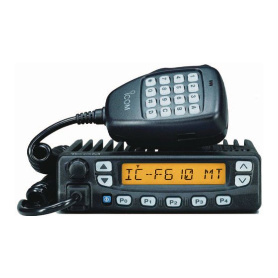
Icom IC-F610 Service Manual
Hide thumbs
Also See for IC-F610:
- Instruction manual (36 pages) ,
- Service manual (6 pages) ,
- Instruction manual (16 pages)
Table of Contents
Advertisement
Quick Links
Advertisement
Table of Contents

Subscribe to Our Youtube Channel
Related Manuals for Icom IC-F610


Summary of Contents for Icom IC-F610
- Page 1 SERVICE MANUAL UHF TRANSCEIVER iF610 iF620 iF621...
- Page 2 VERSION SYMBOL INTRODUCTION Europe This service manual describes the latest service information Europe (MPT) for the IC-F610, IC-F620 and IC-F621 UHF TRANSCEIVERS Europe (BIIS) at the time of publication. IC-F610 General General (MPT) To upgrade quality, any electrical or mechanical parts and...
-
Page 3: Table Of Contents
11 - 2 MAIN UNIT ..............11 - 2 Icom, Icom Inc. and are registered trademarks of Icom Incorporated (Japan) in the United States, the United Kingdom, Germany, France, Spain, Russia and/or other countries. - Page 4 SECTION 1 SPECIFICATIONS USA/GEN Measurement method EIA-152/204D or TIA-603 ETS 300 086 [L-band]: 400.000–430.000 MHz Frequency coverage [M-band]: 440.000–490.000 MHz [H-band]: 480.000–512.000 MHz [USA], 480.000–520.000 MHz [EUR]/[GEN] [N/W]: 8K50F3E/16K0F3E (12.5 kHz; Narrow/25 kHz; Wide) Type of emission [N/M]: 8K50F3E/14K0F3E (12.5 kHz; Narrow/20 kHz; Middle) Max.
- Page 5 SECTION 2 INSIDE VIEW Power module IC3: RA30H4047M-21 [L] Antenna switch/ RA30H4452M-21 [M]-25W, [H] Low-pass filter circuits RA45H4452M-21 [M]-45W 8V regurator (IC9: TA7808F) AF power amplifier 1st mixer* (IC8: LA4425A) (Q3: 3SK272) CPU 5V regurator* 2nd IF filter (IC10: AN78L05M) (FI2: ALFYM450F=K) FM IF IC VCO circuit...
-
Page 6: Front Unit
SECTION 3 DISASSEMBLY INSTRUCTIONS • Removing the front unit Unscrew 4 screws A, and remove the bottom cover. Lift up the front part of the main unit and remove it. Disconnect the flat cable B from J2. Unscrew 2 screws c, and remove the front unit. •... -
Page 7: Main Unit
SECTION 4 CIRCUIT DESCRIPTION 4-1 RECEIVER CIRCUITS 4-1-3 1ST MIXER AND 1ST IF CIRCUITS (MAIN UNIT) 4-1-1 ANTENNA SWITCHING CIRCUIT (MAIN UNIT) The 1st mixer circuit converts the received signals to a fixed The antenna switching circuit functions as a low-pass filter frequency of the 1st IF signal with the PLL output frequency. - Page 8 The 2nd IF signal from the 2nd mixer section (IC1, pin 3) 4-1-6 RECEIVER MUTE CIRCUITS (MAIN UNIT) passes through a ceramic filter (FI2) to remove unwanted • NOISE SQUELCH heterodyned frequencies. It is then amplified at the limiter The noise squelch circuit cuts out AF signals when no RF amplifier section (IC1, pin 5) and applied to the quadrature signals are received.
-
Page 9: Transmitter Circuits
The RF signal from the drive amplifier (Q8) is applied to the fied signals are passed through the compressor, low-pass power module (IC3) to obtain 25 W (for IC-F610/F620, 45 W; filter and high-pass filter sections and then output from pin 9 for IC-F621) of RF power. -
Page 10: Pll Circuits
4-3 PLL CIRCUITS 4-4 POWER SUPPLY CIRCUITS 4-3-1 PLL CIRCUIT LINE DESCRIPTION A PLL circuit provides stable oscillation of the transmit fre- The voltage from a DC power supply. quency and receive 1st LO frequency. The PLL output com- pares the phase of the divided VCO frequency to the refer- The same voltage as the HV line which is ence frequency. -
Page 11: Other Circuits
4-5 OTHER CIRCUITS 4-6 PORT ALLOCATIONS 4-5-1 COMPANDER CIRCUIT (MAIN UNIT) 4-6-1 OUTPUT EXPANDER (FRONT UNIT; IC1) IC-F610 series have compander circuit which can improve S/ Port N ratio and become wide dynamic range. The circuit is com- Description number name posed in the compander IC (IC14). - Page 12 4-6-3 CPU (MAIN UNIT; IC2) Port Port Description Description number name number name I/O port for data signal to the D/A con- Input port for the microphone mute DSDA verter (IC7). signal from the optional unit via J1. MMUT Low: The microphone audio is Outputs strobe signals to the D/A con- DAST muted.
- Page 13 Port Description number name Input port for the MAP27 data signals XTXD from the connected unit via the exter- nal connector (J9). Outputs the MAP27 data signals for XRXD the connected unit via the external connector (J9). Outputs the NMEA data signals for NTXD the connected unit via external con- nector (J8).
-
Page 14: Adjustment Procedures
SECTION 5 ADJUSTMENT PROCEDURES 5-1 PREPARATION When adjusting IC-F610, IC-F620 or IC-F621, one of the following optional adjustment software and JIG CABLE (modified OPC-1122 ; see illustration page 5-5) are required. CLONING CABLE • CS-F500 ADJ (Rev. 2.0 or later): [CONV], [BIIS] versions: •... - Page 15 • CS-F500 ADJ'S SCREEN EXAMPLE CS-F500 ADJ Rev.2.0 File Option COM 1: OPEN Connect Reload (F5) Disp para [A / D] [D / A] : 156 : 9Ch : 12.24 V BPF T1 : 50 : 32h : 0.98 V TEMPS : 187 : BBh : 30.81 'C BPF T2 : 50 : 32h :...
- Page 16 • CS-F600(MPT) ADJ'S SCREEN EXAMPLE CS-F500 ADJ Rev.1.0 File Option COM 1: OPEN Connect Reload (F5) Disp para [A / D] [D / A] : 156 : 9Ch : 12.24 V BPF T1 : 50 : 32h : 0.98 V TEMPS : 187 : BBh : 30.81 'C BPF T2 : 50 : 32h :...
- Page 17 • CS-F620TR ADJ'S SCREEN EXAMPLE NOTE: The above values for settings are example only. Each transceiver has its own specific values for each setting. : Transceiver's connection state : PLL lock voltage : FM deviation : Receive sensitivity (manually) : Reload adjustment data : Operating channel select : CTCSS/DTCS deviation : Reference frequency...
- Page 18 RF power meter DC power supply FM deviation meter Standard signal generator 50 Ω / 1–75 W 13.6 (13.2) V / 20 A (DC measurable) –127 to –17 dBm (0.1 V to 32 mV) Attenuator Frequency 50 dB or 60 dB counter CAUTION: to DC cable...
-
Page 19: Pll Adjustment
5-2 PLL ADJUSTMENT MEASUREMENT ADJUSTMENT ADJUSTMENT ADJUSTMENT CONDITION VALUE UNIT LOCATION UNIT ADJUST PLL LOCK 1 • Operating CH : CH1 MAIN C o n n e c t a d i g i t a l 1.0 V MAIN C133 VOLTAGE •... - Page 20 5-3 SOFTWARE ADJUSTMENT (TRANSMITTING) Select an operation using [↑] / [↓] keys, then set specifi ed value using [←] / [→] keys on the connected computer keyboard. MEASUREMENT ADJUSTMENT ADJUSTMENT CONDITION VALUE UNIT LOCATION REFERENCE 1 • Operating CH : CH7 Rear Loosely couple a frequency 430.0000 MHz [L]...
-
Page 21: Software Adjustment
SOFTWARE ADJUSTMENT (RECEIVING) • Select an operation using [↑] / [↓] keys, then set specifi ed value using [←] / [→] keys on the connected computer keyboard. • Need to adjust "S-METER ADJUSTMENT" after "RX SENSITIVITY ADJUSTMENT" is adjusted. Otherwise , "S-METER ADJUSTMENT" will not be adjusted properly. MEASUREMENT ADJUSTMENT ADJUSTMENT CONDITION... -
Page 22: Front Unit
SECTION 6 PARTS LIST [FRONT UNIT] [FRONT UNIT] ORDER ORDER DESCRIPTION DESCRIPTION LOCATION LOCATION 4030006860 S.CER C1608 JB 1H 102K-T 19/27.4 1130010800 S.IC LC75824W 80.9/24.4 1130008560 S.IC TC75S51F (TE85L) 25.4/22.7 6450002210 3017-8821 <KIN> 6510023090 S.CNR 20FLT-SM1-TB 64.5/25.9 1590000720 S.TR DTA144EUA T106 52.8/22.4 1590000430 S.TR... -
Page 23: Main Unit
[MAIN UNIT] [MAIN UNIT] ORDER ORDER DESCRIPTION DESCRIPTION LOCATION LOCATION 6200003350 S.COL ELJNC R27K-F 81.2/49.7 1590000430 S.TR DTC144EUA T106 16.7/68.3 6110001520 LA-232 [25W] 1540000550 S.TR 2SD1664 T100Q 26.2/58.6 6110002110 LA-382 [45W] 1540000550 S.TR 2SD1664 T100Q 31.2/58.6 6200005680 S.COL ELJRE 15NG-F [M], [H] T 40.3/67.5 1520000460... - Page 24 [MAIN UNIT] [MAIN UNIT] ORDER ORDER DESCRIPTION DESCRIPTION LOCATION LOCATION 7030003570 S.RES ERJ3GEYJ 123 V (12 kΩ) [25W] T 50/64.7 R156 7030003520 S.RES ERJ3GEYJ 472 V (4.7 kΩ) 40.9/63.8 R157 7030003560 S.RES ERJ3GEYJ 103 V (10 kΩ) 41.4/18.7 7030003600 S.RES ERJ3GEYJ 223 V (22 kΩ) [45W] T 50/64.7 S.RES ERJ3GEYJ 151 V (150 Ω)
- Page 25 [MAIN UNIT] [MAIN UNIT] ORDER ORDER DESCRIPTION DESCRIPTION LOCATION LOCATION 4030006860 S.CER C1608 JB 1H 102K-T 90.7/58.8 R267 7030003600 S.RES ERJ3GEYJ 223 V (22 kΩ) 53.1/28.8 4030006860 S.CER C1608 JB 1H 102K-T 82/66.2 R268 7030003650 S.RES ERJ3GEYJ 563 V (56 kΩ) 53.1/27.5 4030009510 S.CER C1608 CH 1H 010B-T...
- Page 26 [MAIN UNIT] [MAIN UNIT] ORDER ORDER DESCRIPTION DESCRIPTION LOCATION LOCATION C114 4030006990 S.CER C1608 CH 1H 080D-T [L], [H] T 62.6/37.8 C214 4030007090 S.CER C1608 CH 1H 470J-T 48.6/14 C215 4030007090 S.CER C1608 CH 1H 470J-T 39.5/14 4030007010 S.CER C1608 CH 1H 100D-T [M] T 62.6/37.8 C115...
- Page 27 [MAIN UNIT] [MAIN UNIT] ORDER ORDER DESCRIPTION DESCRIPTION LOCATION LOCATION 6510021300 S.CNR 52365-1091 21.9/45.7 C321 4030011600 S.CER C1608 JB 1E 104K-T 86.7/22.5 C322 4030006900 S.CER C1608 JB 1H 103K-T 87.3/26.2 C323 4030009880 S.CER C1608 JB 1H 682K-T 89.3/22.2 7120000470 ERDS2T0 C324 4030011600 S.CER C1608 JB 1E 104K-T...
- Page 28 SECTION 7 MECHANICAL PARTS [CHASSIS PARTS] [FRONT UNIT] REF. ORDER REF. ORDER DESCRIPTION QTY. DESCRIPTION QTY. 6510004880 Connector MR-DS-E 01 7210003020 Variable resistor EVU-F2KFK1 6450002210 Connector 3017-8821 2510001030 Speaker VS-57-0837A 8600036860 Cable FX2527 P01CH DS12 5030002780 LCD L1-0483TAT-1 8900010950 Cable OPC-1126 8010018880 2526 chassis 8010018902...
- Page 29 MP11 (C) J1 (C) MP1 (C) MAIN UNIT MP15 (M) MP17 (C) MP12 (C) MP14 (C) MP3 (F) MP12 (M) MP4 (M) MP1 (M) R12 (F) W1 (F) J4 (M) MP13 (M) MP13 (C) J1 (F) W2 (M) MP11 (C) MP3 (F) MP11 (M) MP14 (M)
- Page 30 SECTION 8 SEMI-CONDUCTOR INFORMATION • TRANSSISTORS AND FET’S • DIODES 2SB1132 T100 R 2SC3356 R24 T2B 2SC4116 BL 2SC4213 B 2SC4215 O DA221 TL DAN222TL HVC350B HVC362 MA2S111 (Symbol: BAR) (Symbol: R24) (Symbol: LL) (Symbol: AB) (Symbol: QO) (Symbol: K) (Symbol: N) (Symbol: B0) (Symbol: V2)
- Page 31 SECTION 9 BOARD LAYOUTS 9-1 FRONT UNIT • TOP VIEW VOLUME Horizonal Microphone 9 - 1...
- Page 32 • BOTTOM VIEW (FRONT UNIT) to MAIN unit J2 Horizonal 9 - 2...
- Page 33 9-2 MAIN UNIT • TOP VIEW to DC power to speaker to Optional cable OPC-822 DISC to Optional cable OPC-617 PAAF *except [LTR] HORN* to FRONT unit J2 to Optional unit Horizonal 9 - 3...
- Page 34 • BOTTOM VIEW (MAIN UNIT) Horizonal 9 - 4...
- Page 35 SECTION 10 BLOCK DIAGRAM 2SC4116 DTC144EU MA2S111 XP1214 MAIN UNIT RIPPLE 2SK880 400-520 MHz RX VCO LVIN BUFF D16 HVC350B 2SC4226 RA30H4047M-21 [L] D2 UM9401F RA30H4452M-21 [M]-25W, [H] D14, D15 D5 UM9401F D1, D11 RA45H4452M-21 [M]-45W CR-671A D20 MA2S111 SA7026DH 2SC5107 2SC5107 MA77×2...
- Page 36 SECTION 11 VOLTAGE DIAGRAMS 11-1 FRONT UNIT FRONT UNIT DS12 L1-0483TAT-1 DIM2 SEG22 SEG5 SEG23 SEG4 DTA144EU DTC144EU SEG24 SEG3 SEG25 SEG2 SEG26 SEG1 P12/S12 SEG27 P11/S11 DIM1 SEG28 P10/S10 SEG29 LC75824W P9/S9 SEG30 P8/S8 ON: 7.6V DTC144EU SEG31 HORN DTA144EU DIM: 6.1V P7/S7...
- Page 37 11-2 MAIN UNIT MAIN UNIT (1) BUS LINE1 C366 C378 R209 6.9V 0.001 NTCG20 2SC4116 5.0V 2SK880 R108 3.3k 3.3k IC11 R292 R107 C161 TC75S51F 8.2k C123 100p CR-671A 100k 12p[L] OPV1 R138 APST 2SC4226 8p[M],[H] C145 2SC4215 C372 OPV2 R139 AMSK R307...
- Page 38 CHASSIS MAIN UNIT (2) BUS LINE1 DTC144EU CPU5 R111 R112 C165 0.001 IC21 4.7µ NJM12902V R116 R117 C170 1.5k 5.6k 0.033 R130 27k R131 68k IC21a IC21d C166 NJM12902V R182 R181 R185 NJM12902V IC21b 0.001 C167 C168 C169 C190 NJM12902V 0.027 0.039 0.039...
- Page 39 E-mail : info@icomcanada.com Unit 9, Sea St., Herne Bay, Kent, CT6 8LD, U.K. Phone : +44 (01227) 741741 Fax : +44 (01227) 741742 Icom (Australia) Pty. Ltd. : http://www.icomuk.co.uk E-mail : info@icomuk.co.uk A.B.N. 88 006 092 575 290-294 Albert Street, Brunswick, Victoria, 3056, Australia Icom France S.a...
- Page 40 S-13817HZ-C1U-w C 2002-2005 Icom Inc.
Need help?
Do you have a question about the IC-F610 and is the answer not in the manual?
Questions and answers