Advertisement
Quick Links
EVBUM2277/D
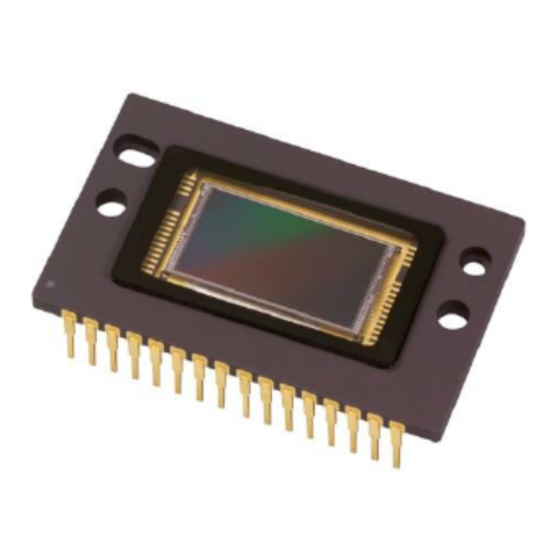
KAI-2093 Image Sensor
Evaluation Timing
Specification
12-bit 20 MHz AFE
Altera Code Version Description
The Altera code described in this document is intended for
use in the KSC−1000 Timing Boar. The code is developed
specifically for use with the following system configuration:
Table 1. SYSTEM CONFIGURATION
Evaluation Board Kit
Timing Generator Board
KAI−2001/KAI−2020/KAI−2093 CCD Imager Board
Framegrabber Board
The 3F5051 Timing Generator Board features the
KSC−1000 Timing Generator chip. The KSC−1000
provides all of the signals necessary for an imaging system
using Full Frame (KAF) or Interline (KAI) family of image
The Altera Programmable Logic Device (PLD) serves as
a state machine, which performs a variety of functions.
Three basic functions are required, common to all CCD
image sensor configurations: serial input steering, AFE
default
programming,
programming. In addition, certain other functions specific to
the KAI−2093 Image Sensor are implemented.
Serial Input Steering
The 3-wire serial interface enters the Timing Board
through the DIO Interface connector, and is routed to the
Table 2. SERIAL INPUT DEVICE SELECT
Device Select DS[2..0]
© Semiconductor Components Industries, LLC, 2014
October, 2014 − Rev. 2
ALTERA CODE FEATURES/FUNCTIONS
and
KSC−1000
default
000
001
010
011
100
101
110
111
EVAL BOARD USER'S MANUAL
PN 4H0706
PN 3F5051 (AD9845A 20 MHz)
PN 3F5121
National Instruments Model PCI−1424
sensors. It also provides the signals necessary for operation
of two analog front-end (AFE) chips, enabling independent
optimization of the AFE chips for dual channel readout
devices.
PLD. The Altera PLD decodes the addressing of the serial
input, and steers the datastream to the correct device.
The serial input must be formatted so that the Altera PLD
can correctly decode and steer the data to the correct device.
The serial interface can be used to dynamically change the
operating conditions of the AFE or KSC−1000 chips by
reprogramming the appropriate registers. Reprogramming
these registers through the serial interface will have no effect
on the default settings that are automatically programmed
into these devices on power-up or board reset.
Serial Device
KSC−1000
(Not Used)
(Not Used)
(Not Used)
(Not Used)
1
www.onsemi.com
PLD
AFE1
AFE2
Publication Order Number:
EVBUM2277/D
Advertisement

Related Manuals for ON Semiconductor KAI-2093


Summary of Contents for ON Semiconductor KAI-2093
- Page 1 EVBUM2277/D KAI-2093 Image Sensor Evaluation Timing Specification 12-bit 20 MHz AFE www.onsemi.com Altera Code Version Description EVAL BOARD USER’S MANUAL The Altera code described in this document is intended for use in the KSC−1000 Timing Boar. The code is developed specifically for use with the following system configuration: Table 1.
- Page 2 EVBUM2277/D … SLOAD_INPUT (decoded PLD output) SLOAD_xxx Ï Ï Ï Ï Ï Ï Ï Ï Ï Ï Ï Ï Ï Ï Ï SDATA_INPUT Ï Ï Ï Ï Ï Ï Ï Ï Ï Ï Ï Ï Ï Ï Ï SCLK_INPUT Figure 1. Serial Input Timing The first 3 bits in the datastream are the Device Select bits The remaining bits in the bitstream are Data bits, LSB DS[2..0], sent MSB first, as shown in Figure 1.
- Page 3 EVBUM2277/D … Ï Ï Ï Ï Ï Ï Ï Ï Ï Ï Ï Ï Ï Ï Ï SLOAD_TG Ï Ï Ï Ï Ï Ï Ï Ï Ï Ï Ï Ï Ï Ï SDATA Ï Ï Ï Ï Ï Ï Ï Ï...
- Page 4 EVBUM2277/D effect, either by pressing the BOARD_RESET button (S1) Binning Control PLD input SW2 is used to select between 2×2 Binning on the Timing Board, or by setting and resetting the Remote Single Output, and normal operation (no binning). When Reset (DIO14) input.
- Page 5 EVBUM2277/D Outputs The Altera PLD outputs include: the 3-wire serial synchronization; the PLD[2..0] signals which are auxiliary interface; control signals KSC−1000; Imager Board control bits; and the GIO[2..0] bits which are the INTEGRATE signal used for external monitoring and used for PLD monitoring and testing. Table 5.
-
Page 6: Modes Of Operation
EVBUM2277/D Table 7. CCD TIMING (continued) Pixel Counts Description Symbol Time Notes 25.05 ms VCCS Pedestal Time 12.30 ms Photodiode Transfer Time V2 3 Level 20.00 ms Photodiode Delay 85.50 ms Photodiode Frame Delay 1710 Delay before 1 Line Transfer 142.85 ms Photodiode Transfer Period 2857... - Page 7 EVBUM2277/D Table 9. DEFAULT AD9845A AFE REGISTER PROGRAMMING Register Value Address (decimal) Description Notes Operation VGA Gain Corresponds to a VGA Stage Gain of 9.9 dB (KAI−2093) Clamp The Output of the AD9845A will be Clamped to Code 96 during the CLPOB Period Control CDS Gain Enabled 4, 5, 6, 7...
- Page 8 EVBUM2277/D Table 11. REGISTER 1 DEFAULT SETTING (continued) Register Entry Data (1-channel) Data (2-channel) DATACLK1_Enable DATACLK2_Enable PIXCLK_Enable H3_Enable H1_Enable H2_Enable SH1_Enable SH3_Enable H6 24 mA Output Enable H4 24 mA Output Enable H5 24 mA Output Enable RG 24 mA Output Enable SH2 24 mA Output Enable SH4 24 mA Output Enable DATACLK1 24 mA Output Enable...
- Page 9 EVBUM2277/D Register 4: INTG_START Line Short integration times may be controlled through use of values are chosen to allow integration times adjustable in the Electronic Shutter. The default setting written to increments of one-eighth the Frame or Flush time. Register 4 controls the line number on which the Electronic If the line number is greater than the number of lines Shutter will occur.
- Page 10 EVBUM2277/D Table 15. REGISTER 5 DEFAULT SETTING (continued) Register Entry 1-channel 2-channel Evaluation Board Signal Name V3_IDLE_VAL V4_IDLE_VAL V5_IDLE_VAL (Not Used) V6_IDLE_VAL Register 6: Pixel-Rate Signal Offset The default settings written to Register 6 depend on the position of SW0 on the Timing Board, used to select between 1-channel and 2-channel operation.
- Page 11 EVBUM2277/D Register 8: Frame Tables Several Frame Tables are written by default to the Frame Table 1 is used for Single Channel 2×2 Binning KSC−1000 Frame Table registers, but only one Frame Table mode. Note that the last row in Table 18 and Table 19 are the is active at one time, as determined by the Frame Table mnemonics associated with the Flag, Count, and Address Pointer...
- Page 12 EVBUM2277/D Table 19. FRAME TABLE 1 DEFAULT SETTING (continued) FT1 Entry Bit Location Bit Location Frame Table Data Frame Table Data CLPOB1 Enable PBLK Enable Pblk_Idle_Val Flag 17:29 Count 30:32 Address 2:0 Address 3 − Mnemonic ELT0 ExLTNVD 5 ELT 1 JMPFT 1 Register 9: Line Tables There are five Line Tables written by default to the...
- Page 13 EVBUM2277/D Line Table 2 is the Integration sequence. The vertical clocks are not active, and the Horizontal register is continually flushed of charge. See Figure 6. Table 22. LINE TABLE 2 DEFAULT SETTING LT2 Entry CCD Signal Line Table Data Name Count[0..12] HCLK_H Enable V3RD...
- Page 14 EVBUM2277/D KAI−2093 TIMING Line Table 0 (Line Transfer) Line Table 0 is the Line Transfer timing sequence that is moved down the vertical CCD registers, and the last row transfers one entire row of charge toward the horizontal of charge is dumped into the horizontal register. The VCCD register.
- Page 15 EVBUM2277/D Line Table 2 (Integration) clocks are running continuously. This sequence runs until Line Table 2 is the Integration timing sequence, during Integration is complete, signaled by the assertion of the which the Vertical clocks are inactive and the Horizontal VD_TG signal from the Altera PLD.
- Page 16 EVBUM2277/D Frame Table 0 Sequence Frame Table 0 contains the Free-Running (video mode) integration is complete, the Altera PLD asserts the VD_TG timing sequence used to continuously read out all rows of the signal to the KSC−1000. This initiates the Photodiode CCD.
- Page 17 EVBUM2277/D V1_CCD V2_CCD H1A_CCD H2A_CCD CLPOB1 PBLK INTEGRATE VD_TG FRAME_VALID LINE_VALID FT0 Entry Line Table 1104 Counts PLD STATE V_TRANSFER TIMED_INTEGRATION DIODE_TRANSFER (not to scale) Figure 10. Frame Table 0 Default Timing Frame Table 1 Sequence Frame Table 1 contains the 2×2 Binning Mode timing Frame Table 0, except that the Vertical Clocks are asserted sequence used to sum the charge collected in four photosites twice per line, which dumps charge from two vertical CCD...
- Page 18 EVBUM2277/D V1_CCD V2_CCD Start of Integration VSUB H1A_CCD H2A_CCD setup width hold Reg3 Entry (Line Table 0) Pix Counts (not to scale) Figure 12. Electronic Shutter Timing Horizontal Timing Figure 13 depicts the basic theoretical relationship between the pixel-rate clocks to the CCD, the Video output of the CCD, and the pixel-rate clocks to the AFE.
- Page 19 EVBUM2277/D The Altera PLD default KSC−1000 settings contain 2×2 Pointer (Register 0) must be changed to a value of 2. This is Binning Mode timing in Frame Table 2 (See Figure 11). In done by setting SW2 HIGH and pressing the order to activate the 2×2 Binning Mode, the Frame Table BOARD_RESET button (S1 on the Timing Board).
- Page 20 EVBUM2277/D Table 25. PROGRAMMED INTEGRATION TIMES DIO[11..7] Int Count Free-Run Mode Reg4 Entry Free-Run Mode Tint(s) 0 (Default) 2040 (No Shutter) 0.115 0.014 0.029 0.043 0.057 0.072 0.086 0.101 2040 (No Shutter) 0.116 2040 (No Shutter) 0.118 2040 (No Shutter) 0.120 2040 (No Shutter) 0.125...
- Page 21 EVBUM2277/D Figure 15. Programmed Integration Times V1_CCD 1103 1104 V2_CCD VES (shutter) Shutter Line = 2040 (No shutter pulse) INTEGRATE 1ms Clock Integration Count = 0 VD_TG FRAME_VALID LINE_VALID FT0 Entry Line Table 1104 Counts DIO[11..7] (not to scale) Figure 16. Free-Running Mode Default Integration Timing http://onsemi.com...
- Page 22 EVBUM2277/D V1_CCD 965 966 1103 1104 V2_CCD VES (shutter) INTEGRATE 1ms Clock Integration Count = 0 VD_TG FRAME_VALID LINE_VALID FT0 Entry Line Table 1104 Counts DIO[11..7] 1 (Shutter Line = 966) (not to scale) Figure 17. Free-Running Mode Integration Timing with Shutter V1_CCD V2_CCD VES (shutter)
- Page 23 EVBUM2277/D BOARD INTERFACE CONNECTOR SIGNAL MAP For reference, the board interface timing signals from the shown in Table 26. Note that the power connections are not 3F5051 Timing Board to the 3F5121 Imager Board are shown here. Table 26. TIMING BOARD/IMAGER BOARD SIGNAL MAP KSC−1000 Timing Board KAI−2093 Imager Board KSC−1000...
-
Page 24: Warnings And Advisories
Board during the reprogramming of the Altera PLD, damage customer. to the Imager Board will occur. Purchasers of a ON Semiconductor Evaluation Board Kit may, at their discretion, make changes to the Timing ORDERING INFORMATION Please address all inquiries and purchase orders to:... -
Page 25: User Manual
PUBLICATION ORDERING INFORMATION LITERATURE FULFILLMENT: N. American Technical Support: 800−282−9855 Toll Free ON Semiconductor Website: www.onsemi.com Literature Distribution Center for ON Semiconductor USA/Canada Order Literature: http://www.onsemi.com/orderlit P.O. Box 5163, Denver, Colorado 80217 USA Europe, Middle East and Africa Technical Support: Phone: 303−675−2175 or 800−344−3860 Toll Free USA/Canada...
Need help?
Do you have a question about the KAI-2093 and is the answer not in the manual?
Questions and answers