
Related Manuals for IEI Technology ICPMB-8650


Summary of Contents for IEI Technology ICPMB-8650
- Page 1 ICPMB-8650 SOCKET 478 PENTIUM 4 Motherboard with SATA & Ethernet & USB 2.0 Manual Rev: 1.1 ©Copyright 2005 by IEI Electronics Inc. All Rights Reserved.
-
Page 2: Copyright Notice
Copyright Notice The information in this document is subject to change with out prior notice in order to improve reliability, design and function and does not represent a commitment on the part of the manufacturer. In no event will the manufacturer be liable for direct, indirect, special, incidental, or consequential damages arising out of the use or inability to use the product or documentation, even if advised of the possibility of such damages. -
Page 3: Table Of Contents
Specifications ..............2 What You Have ..............4 Installation ..................5 ICPMB-8650’s Layout ............6 ICPMB-8650’s Dimensions (Unit : mm)........ 7 Unpacking Precautions ............8 Clear CMOS Setup............9 COM3 RS232 or RS422/485 Selection ........ 9 Compact Flash Master/Slave Function Setting ..... 9 Connection.................. - Page 4 Advanced BIOS Features ..........31 Advanced Chipset Features ..........35 Integrated Peripherals ............37 Power Management Setup ..........42 4.10 PnP/PCI Configuration Setup..........45 4.11 PC Health Status ............46 4.12 Frequency/Voltage Control ..........47 4.13 Load Fail-Safe Defaults ............ 48 4.14 Load Optimized Defaults ..........
-
Page 5: Introduction
,but it’s not support any 3.3V AGP-card. The integrated graphics controller provides 3D, 2D, and display capabilities. ICPMB-8650 is supports one or two 64-bit wide DDR data channels. Available bandwidth up to 2.7GB/s for single-channel mode and 5.4GB/s in dual-channel mode. -
Page 6: Specifications
1.1 Specifications Intel Pentium 4 Processor, supports CPU(PGA 478) 400/533/800 MHz PSB (set by BIOS) AGP/PCI/ISA bus Bus interface Bus speed PCI: 33Mhz,ISA: 8Mhz DMA channels Interrupt levels Chipset INTEL 865G / ICH5 Four 184-pin DIMM sockets support DDR333/400 SDRAM .Support one or four 64-bit RAM memory wide DDR data channels. - Page 7 expansion Software Programmable, reset generated when Watchdog timer CPU does not periodically trigger the timer. Supports two independent serial ATA Serial ATA channels. Data transfer rate is up to 150MB/s PCI interface. INTEL 82540EM or Realtek Ethernet RTL8110S Gigabit Ethernet controller. Supports full 10,100 and1000-bast-T Ethernet A connector is located on the mounting bracket Keyboard and PS/2...
-
Page 8: What You Have
1.2 What You Have In addition to this User's Manual, the ICPMB-8650 package includes the following items: • ICPMB-8650 Single Board Computer X1. • RS-232 Cable with bracket X3. • FDD cable X1. • PATA IDE cable X2. • SATA IDE cable X2. -
Page 9: Installation
Installation This chapter describes how to install the ICPMB-8650. First a layout diagram of the ICPMB-8650 is shown, followed by unpacking information that should be carefully followed. The jumpers and switch settings for the ICPMB-8650 configuration, such as CPU type selection, system clock setting, and... -
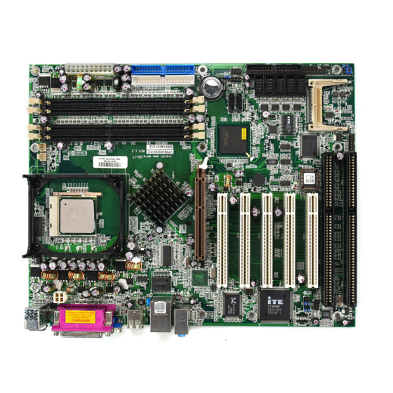
Page 10: Icpmb-8650'S Layout
ICPMB-8650’ s Layout... -
Page 11: Icpmb-8650'S Dimensions (Unit : Mm)
ICPMB-8650’ s Dimensions (Unit : mm) -
Page 12: Unpacking Precautions
ü Ground yourself to remove any static charge before touching your ICPMB-8650. You can do it by using a grounded wrist strap at all times or by frequently touching any conducting materials that is connected to the ground. -
Page 13: Clear Cmos Setup
2.4 Clear CMOS Setup To clear the CMOS Setup (e.g., you have forgotten the password, you must clear the CMOS to reset the password), you have to close the JP1 (pin 2-3) for about 3 seconds, then open it. After that, pin 1-2 has to be short for normal operation. -
Page 14: Connection
Connection This chapter describes how to connect peripherals, switches and indicators to the ICPMB-8650 board. Label Function IDE1 & IDE2 Ultra ATA100 Primary & Secondary IDE connectors FDD1 Floppy connector PRN1 Parallel port connector COM1,2,3,4,5,6 Serial port connectors Compact Flash Storage Card Type II connector... -
Page 15: Pci E-Ide Disk Drive Connector
3.1 PCI E-IDE Disk Drive Connector You can attach up to four IDE( Integrated Device Electronics) devices. • IDE1 : Primary IDE Connector • IDE2 : Secondary IDE Connector DESCRIPTION DESCRIPTION RESET# GROUND DATA 7 DATA 8 DATA 6 DATA 9 DATA 5 DATA 10 DATA 4... -
Page 16: Floppy Connector
3.2 Floppy Connector The ICPMB-8650 board is equipped with a 34-pin daisy-chain drive connector cable. • FDD1 : Floppy Connector DESCRIPTION DESCRIPTION GROUND RWC0- GROUND GROUND RWC1- GROUND INDEX- GROUND MO-A GROUND DS-B GROUND DS-A GROUND MO-B GROUND DIR- GROUND... -
Page 17: Parallel Port Connector
3.3 Parallel Port Connector Usually, a printer is connected to the parallel port. The ICPMB- 8650 includes an on-board parallel port • PRN1 : Parallel Port Connector DESCRIPTION DESCRIPTION STROBE# DATA 0 DATA 1 DATA 2 DATA 3 DATA 4 DATA 5 DATA 6 DATA 7... -
Page 18: Serial Port
3.4 Serial Port The ICPMB-8650 offers Six high speed NS16C550 compatible UART’s with 16-byte Read/Receive FIFO serial ports. • COM1: D-SUB Serial Port Connector DESCRIPTION DESCRIPTION GROUND • COM2,3,4,5,6: Serial Port Connector DESCRIPTION DESCRIPTION GROUND GROUND... -
Page 19: Compact Flash Storage Card Socket
Compact Flash Storage Card Socket The ICPMB-8650 configures Compact Flash Storage Card in IDE Mode. This type II Socket is compatible with IBM Micro Drive. • CF1 : Compact Flash Storage Card Socket pin assignment PIN NO. DESCRIPTION PIN NO. -
Page 20: Irda Infrared Interface Port
3.6 IrDA Infrared Interface Port The ICPMB-8650 comes with an integrated IrDA port which supports either a Serial Infrared(SIR) or an Amplitude Shift Keyed IR(ASKIR) interface. • IR1: IrDA connector DESCRIPTION IR-RX Ground IR-TX CIRRX 3.7 USB Port Connector The ICPMB-8650 is equipped with Eight USB(Version. 2.0) ports for the future new I/O bus expansion. -
Page 21: Keyboard/Mouse Connector
• CN2 : 2 ports USB Connector PIN DESCRIPTION DESCRIPTION DATA6- DATA7- DATA6+ DATA7+ GROUND GROUND 3.8 Keyboard/Mouse Connector The ICPMB-8650 has a keyboard/mouse connector • KB/MS1 : Keyboard/Mouse Connector PIN DESCRIPTION PIN DESCRIPTION KB DATA MS DATA GROUND GROUND KB VCC MS VCC KB CLOCK... -
Page 22: Fan Connector
3.9 Fan Connector The ICPMB-8650 also has a CPU with cooling fan connector and chassis fan connector, which can supply 12V/500mA to the cooling fan. There is a “rotation” pin in the fan connector, which transfers the fan’s rotation signal to the system BIOS in order to recognize the fan speed. -
Page 23: Vga Connector
VCC / NC GROUND DDC DAT HSYNC VSYNC DDCCLK 3.12 LAN Connector ICPMB-8650 equipped with Ethernet Controllers 10/100Mbps, which are connected to the LAN via an RJ45 LAN connector. The pin assignments are as follows: • CN2 : RJ45 Connector (10/100/1000) -
Page 24: Audio Connector
3.13 Audio Connector The onboard AC’97 CODEC supports several audio functions. The audio connectors are described below. • CN1 : Audio connector ( Line in, Line out, MIC in) • CN3 : Audio AUX In connector DESCRIPTION AUX (LEFT) GROUND GROUND AUX (RIGHT) •... -
Page 25: Atx +12V Power Connector
• CN7 : Front Panel Audio connector PIN DESCRIPTION PIN DESCRIPTION MIC IN GROUND MIC BIAS LINE OUT(R) LINE OUT (R) Return LINE OUT(L) LINE OUT (L) Return • CN8 : S/PDIF connector DESCRIPTION S/PDIF OUT GROUND S/PDIF IN 3.14 ATX +12V Power connector •... -
Page 26: Ibutton Connector
3.15 iButton connector • CN9: I button connector DESCRIPTION DESCRIPTION iButton GROUND input/output 3.16 Digital I/O connector • CN10: Digital I/O connector DESCRIPTION DESCRIPTION DGPI0 DGPO0 DGPI1 DGPO1 DGPI2 DGPO2 DGPI3 DGPO3 DGPI4 DGPO4 DGPI5 DGPO5 DGPI6 DGPO6 DGPI7 DGPO7 GROUND... -
Page 27: External Switches And Indicators
3.17 External Switches and Indicators There are several external switches and indicators for monitoring and controlling your CPU board. All functions are in the CN11connector. • CN11 : Pin Assignment and Functions FUNCTION DESCRIPTION BUZZER BUZZER- RESET RESET GROUND HDD LED IDE_LED+ IDE_LED- POWER LED... -
Page 28: Rs422/485 Connector
3.18 RS422/485 connector • CN12: RS422/485 connector DESCRIPTION 3.19 ATX Power connector • ATX1: ATX Power connector DESCRIPTION DESCRIPTION VCC3 VCC3 VCC3 -12V GROUND GROUND PS-ON GROUND GROUND GROUND GROUND GROUND POWER GOOD 5VSB +12V... -
Page 29: Award Bios Setup
Award BIOS Setup 4.1 Introduction This chapter discusses the Setup program written in the BIOS. It will give you a step-by-step guidance to configure your system. The user- defined configuration is then stored in battery-backed CMOS RAM, which retains the customized information while the power is off. 4.2 Starting Setup The BIOS is immediately active when you turn on the computer. -
Page 30: Using Setup
4.3 Using Setup In general, you can use the arrow keys to highlight items, press <Enter> to select, use the PageUp and PageDown keys to change entries, press <F1> for help and press <Esc> to quit. The following table provides more details about how to navigate in the Setup program using the keyboard. -
Page 31: Main Menu
4.4 Main Menu Once you enter the AwardBIOS™ CMOS Setup Utility, the Main Menu will appear on the screen. The Main Menu allows you to select from several setup functions and two exit choices. Use the arrow keys to go through the items and press <Enter>... - Page 32 Advanced Chipset Features Use this menu to change the values in the chipset registers and optimize your system's performance. See section 4.7 for the details. Integrated Peripherals Use this menu to configure your settings for integrated peripherals. See section 4.8 for the details. Power Management Setup Use this menu to configure your settings for power management.
-
Page 33: Standard Cmos Setup
change these defaults to meet their needs. See section 4.14 for the details. Set Password Use this menu to set Passwords. See section 4.15 for the details. Save & Exit Setup Save CMOS value changes to CMOS and exit setup. See section 4.16 for the details. - Page 34 Time HH : MM : SS Set the system time Options are in its sub Press <Enter> to enter the Primary Master menu menu detailed (described in Table 3) options Options are in its sub Press <Enter> to enter the Primary Slave menu menu...
-
Page 35: Advanced Bios Features
this menu. IDE Primary Master None Selecting ‘manual’ lets you Auto set the remaining fields on Manual this screen. Selects the type of fixed disk. "User Type" will let you select the number of cylinders, heads, etc. Note: PRECOMP=65535 means NONE ! Capacity Auto Display your disk... - Page 36 Enabled Activates automatically when the system boots up causing a warning message to appear when anything attempts to access the boot sector or hard disk partition table. Disabled No warning message will appear when anything attempts to access the boot sector or hard disk partition table. Hard Disk Boot Priority This setting is to select hard disk boot priority CPU L1 &...
- Page 37 Enabled Enable quick POST Disabled Normal POST First/Second/Third/Other Boot Device The BIOS attempts to load the operating system from the devices in the sequence selected in these items. The Choice: Floppy, LS120, HDD0-3, SCSI, CDROM, ZIP 100 , LAN, Disabled. Swap Floppy Drive If the system has two floppy drives, you can swap the logical drive name assignments.
- Page 38 The choice: Enabled/Disabled. Typematic Rate (Chars/Sec) Sets the number of times a second to repeat a key stroke when you hold the key down. The choice: 6, 8, 10, 12, 15, 20, 24, 30. Typematic Delay (Msec) Sets the delay time after the key is held down before it begins to repeat the keystroke.
-
Page 39: Advanced Chipset Features
4.7 Advanced Chipset Features This section allows you to configure the system based on the specific features of the installed chipset. This chipset manages bus speeds and access to system memory resources, such as DRAM and the external cache. It also coordinates communications between the conventional ISA bus and the PCI bus. - Page 40 DRAM RAS# to CAS# Delay This field lets you insert a timing delay between the CAS and RAS strobe signals, used when DRAM is written to, read from, or refreshed. Fast gives faster performance; and Slow gives more stable performance. This field applies only when synchronous DRAM is installed in the system.
-
Page 41: Integrated Peripherals
Memory Hole At 15M-16M You can reserve this area of system memory for ISA adapter ROM. When this area is reserved, it cannot be cached. The user information of peripherals that need to use this area of system memory usually discusses their memory requirements. - Page 43 On-Chip Primary/Secondary PCI IDE The integrated peripheral controller contains an IDE interface with support for two IDE channels. Select Enabled to activate each channel separately. The choice: Enabled, Disabled. IDE Primary/Secondary Master/Slave PIO The four IDE PIO (Programmed Input/Output) fields let you set a PIO mode (0-4) for each of the four IDE devices that the onboard IDE interface supports.
- Page 44 The Choice: Auto, Disabled. On-Chip Serial ATA [Disable] : Disable SATA controller. [Combined] : SATA and PATS are combined. Max. of 2 IDE drivers in each channel. [Enhanced] : Enhanced both SATA and PATA. Max. of 6 IDE drivers are support.
- Page 45 The choice: Enabled, Disabled Onboard Serial Port 1/Port 2 Select an address and corresponding interrupt for the first and second serial ports. The choice: 3F8/IRQ4, 2E8/IRQ3, 3E8/IRQ4, 2F8/IRQ3, Disabled, Auto UART Mode Select Select a serial port 2 operation mode. The choice: Normal, IrDA, ASKIR, SCR Onboard Parallel Port Select an address and corresponding interrupt for the parallel ports.
-
Page 46: Power Management Setup
4.9 Power Management Setup The Power Management Setup allows you to configure you system to most effectively save energy while operating in a manner consistent with your own style of computer use. ACPI Function This feature is switch of ACPI function. Configuration options: Enable/Disable. - Page 47 Power Management This category allows you to select the type (or degree) of power saving and is directly related to the following modes: Min. Power Saving Minimum power management. Doze Mode = 1 hr. Standby Mode = 1 hr., Suspend Mode = 1 hr., and HDD Power Down = 15 min.
- Page 48 Suspend Mode When enabled and after the set time of system inactivity, all devices except the CPU will be shut off. The choice: 1Min, 2Min, 4Min, 8Min, 12Min, 20Min, 30Min, 40Min, 1Hour, Disabled HDD Power Down When enabled and after the set time of system inactivity, the hard disk drive will be powered down while all other devices remain active.
-
Page 49: Pnp/Pci Configuration Setup
4.10 PnP/PCI Configuration Setup This section describes configuring the PCI bus system. PCI, or Personal Computer Interconnect, is a system which allows I/O devices to operate at speeds nearing the speed the CPU itself uses when communicating with its own special components. This section covers some very technical items and it is strongly recommended that only experienced users should make any changes to the default settings. -
Page 50: Pc Health Status
this capability means absolutely nothing unless you are using a Plug and Play operating system such as Windows®95. If you set this field to “manual” choose specific resources by going into each of the sub menu that follows this field (a sub menu is preceded by a “ Ø”). The choice: Auto(ESCD), Manual. -
Page 51: Frequency/Voltage Control
4.12 Frequency/Voltage Control Auto Detect DIMM/PCI Clk This item allows you to enable/disable auto detect DIMM/PCI Clock. The choice: Enabled, Disabled. Spread Spectrum This item allows you to enable/disable the spread spectrum modulate. The choice: Enabled, Disabled. -
Page 52: Load Fail-Safe Defaults
4.13 Load Fail-Safe Defaults When you press <Enter> on this item you get a confirmation dialog box with a message similar to: Load Fail-Safe Defaults (Y/N) ? N Pressing ‘Y’ loads the BIOS default values for the most stable, minimal- performance system operations. -
Page 53: Set Password
4.15 Set Password can enter and change the options of the setup menus. ENTER PASSWORD: Type the password, up to eight characters in length, and press <Enter>. The password typed now will clear any previously entered password from CMOS memory. You will be asked to confirm the password. Type the password again and press <Enter>. -
Page 54: Exit Selecting
4.16 Exit Selecting Save & Exit Setup Pressing <Enter> on this item asks for confirmation: Save to CMOS and EXIT (Y/N)? Y Pressing “Y” stores the selections made in the menus in CMOS – a special section of memory that stays on after you turn your system off. The next time you boot your computer, the BIOS configures your system according to the Setup selections stored in CMOS. -
Page 55: Appendix A. Watchdog Timer
Appendix A. Watchdog Timer The Watchdog Timer is provided to ensure that standalone systems can always recover from catastrophic conditions that cause the CPU to crash. This condition may have occurred by external EMI or a software bug. When the CPU stops working correctly, hardware on the board will either perform a hardware reset (cold boot) or a Non-Maskable Interrupt (NMI) to bring the system back to a known state. - Page 56 Example program: ; INITIAL TIMER PERIOD COUNTER W_LOOP: AX, 6F02H ;setting the time-out value BL, 30 ;time-out value is 48 seconds ; ADD YOUR APPLICATION PROGRAM HERE EXIT_AP, 1 ;is your application over? W_LOOP ;No, restart your application AX, 6F02H ;disable Watchdog Timer BL, 0 ;...
-
Page 57: Appendix B. Address Mapping
Appendix B. Address Mapping IO Address Map I/O address Range Description 000-01F DMA Controller 020-021 Interrupt Controller 040-05F System time 060-06F Keyboard Controller 070-07F System CMOS/Real time Clock 080-09F DMA Controller 0A0-0A1 Interrupt Controller 0C0-0DF DMA Controller 0F0-0FF Numeric data processor 1F0-1F7 Primary IDE Channal 2E8-2EF... -
Page 58: Dma Channel Assignments
1st MB Memory Address Map Memory address Description 00000-9FFFF System memory A0000-BFFFF VGA buffer F0000-FFFFF System BIOS 1000000- Extend BIOS *Default setting IRQ Mapping Table IRQ0 System Timer IRQ8 RTC clock IRQ1 Keyboard IRQ9 AUDIO/SMBus Cntrlr IRQ2 Available IRQ10 COM4/COM6 IRQ3 COM2 IRQ11... -
Page 59: Appendix C. How To Upgrade A New Bios
Appendix C. How to Upgrade a New BIOS <Note> Before flashing BIOS , please enable the item “FLASH BIOS” in BIOS setting. You can install an upgrade BIOS for the that you can SAGP-865EVG download from the manufacturer’ s web site ). - Page 60 5. At the DOS command prompt type , "awdflash filename.xxx", where filename.xxx is the file name of the BIOS file . Hit enter. 6. Your first option, in sequence, will be to save the old BIOS. We recommend that you do that in case, for whatever reason, you decide you don't wish to use the new version once it is installed.
- Page 61 initial boot-up screen has changed to the new BIOS version. Your BIOS upgrade is now complete. Recovering Your Old BIOS: 1. Assuming you have the floppy made during the upgrade procedure noted above, boot the system with that diskette in the floppy drive.
-
Page 62: Appendix D. Install Memory Modules
Appendix D. Install memory modules ICPMB-8650 has four dual in line memory module (DIMM) sockets . The BIOS will automatically detects memory type and size. To ins tall the memory module, just push it vertically into the DIMM socket. The DIMM module can only fit in one direction due to the notch.
Need help?
Do you have a question about the ICPMB-8650 and is the answer not in the manual?
Questions and answers