Table of Contents
Advertisement
Quick Links
Advertisement
Table of Contents

Related Manuals for Phytec phycore i.mx7


Summary of Contents for Phytec phycore i.mx7
- Page 1 A product of a PHYTEC Technology Holding company...
-
Page 2: Pcm-061/Phycore-I.mx7 System On Module L-821E
Additionally, PHYTEC America L.L.C. offers no guarantee nor accepts any liability for damages arising from the improper usage or improper installation of the hardware or software. PHYTEC America L.L.C. further reserves the right to alter the layout and/or design of the hardware without prior notification and accepts no liability for doing so. -
Page 3: Table Of Contents
QSPI NOR Flash Memory (U9) ........................... 35 Memory Model ..............................35 SD/MMC Card Interfaces ............................36 Serial Interfaces................................. 37 USB ..................................37 Ethernet ................................37 C ..................................38 PCI Express ................................ 38 Debug Interface..............................39 © PHYTEC America L.L.C. 2017... - Page 4 PCM-061/phyCORE-i.MX7 System on Module L-821e_2 Technical Specifications ............................40 Hints for Integrating and Handling the phyCORE-i.MX7 ..................42 12.1 Integrating the phyCORE-i.MX7 ........................42 12.2 Handling the phyCORE-i.MX7 ........................... 42 Revision History..............................43 © PHYTEC America L.L.C. 2017...
-
Page 5: List Of Figures
Figure 4. Pinout of the phyCORE-Connector (top view, with cross section insert) ............. 18 Figure 5. Jumper Numbering Schemes ..........................25 Figure 6. Power Supply Diagram ............................28 Figure 7. phyCORE-i.MX7 Mechanical Dimensions (profile view)..................40 © PHYTEC America L.L.C. 2017... -
Page 6: List Of Tables
Table 10. SD/MMC Boot Configuration Description ......................33 Table 11. I2C1 Reserved Addresses ............................. 38 Table 12. Technical Specifications............................41 Table 13. Recommended Operating Conditions for the Input and Output Power Domains ..........41 Table 14. Revision History ..............................43 © PHYTEC America L.L.C. 2017... -
Page 7: Conventions, Abbreviations And Acronyms
Text in blue italic indicates a hyperlink within, or external to the document. Click these links to quickly jump to the applicable URL, part, chapter, table, or figure. • References made to the phyCORE-Connector always refer to the high density Samtec connectors on the undersides of the phyCORE-i.MX7 © PHYTEC America L.L.C. 2017... -
Page 8: Table 1. Abbreviations And Acronyms Used In This Manual
3.3V tolerant input with pull-down 3V3_PD LVDS Differential line pairs 100 Ohm LVDS LVDS Differential 90 Ohm Differential line pairs 90 Ohm DIFF90 Differential 100 Ohm Differential line pairs 100 Ohm DIFF100 Analog Analog input or output Analog © PHYTEC America L.L.C. 2017... -
Page 9: Preface
The part numbering of the phyCORE-i.MX7 has the following structure This structure shows the ordering options available as of the printing of this manual. Additional ordering options may have been added. Please contact our sales team to check current availability, inventory, and lead-time. © PHYTEC America L.L.C. 2017... - Page 10 The phyCORE-i.MX7 is one of a series of PHYTEC System on Modules that can be populated with different controllers and, hence, offers various functions and configurations. PHYTEC supports a variety of 8-/16- and 32-bit controllers in two ways: 1.
-
Page 11: Product Change Management
In addition to our HW and SW offerings, the buyer will receive a free obsolescence maintenance service for the HW provided when purchasing a PHYTEC SOM. Our Product Change Management Team of developers is continuously processing all incoming PCN's (Product Change Notifications) from vendors and distributors concerning parts which are being used in our products. -
Page 12: Introduction
L-821e_2 Introduction The phyCORE-i.MX7 belongs to PHYTEC’s phyCORE System on Module family. The phyCORE SOMs represent the continuous development of PHYTEC System on Module technology. Like its mini-, micro- and nanoMODULE predecessors, the phyCORE boards integrate all core elements of a microcontroller system on a subminiature board and are designed in a manner that ensures their easy expansion and embedding in peripheral hardware development. - Page 13 4x ADC • 3x Tamper • 3x PWM • 1x SAI • 1x QSPI • Keypad (3x3) • JTAG • GPIO Highly multiplexed. All ports may not be available at once depending on use case. © PHYTEC America L.L.C. 2017...
-
Page 14: Block Diagram
PCM-061/phyCORE-i.MX7 System on Module L-821e_2 Block Diagram Figure 1. phyCORE-i.MX7 Block Diagram © PHYTEC America L.L.C. 2017... -
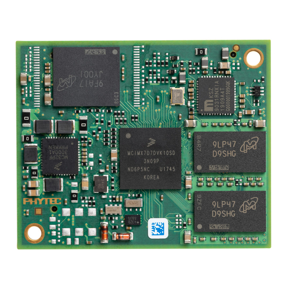
Page 15: Component Placement Diagram
PCM-061/phyCORE-i.MX7 System on Module L-821e_2 Component Placement Diagram Figure 2. phyCORE-i.MX7 Component Placement (top view) Detailed component placement diagrams with all reference designators are available through our website © PHYTEC America L.L.C. 2017... -
Page 16: Figure 3. Phycore-I.mx7 Component Placement (Bottom View)
PCM-061/phyCORE-i.MX7 System on Module L-821e_2 Figure 3. phyCORE-i.MX7 Component Placement (bottom view) © PHYTEC America L.L.C. 2017... -
Page 17: Pin Description
(defined with dotted lines) as it would be mounted on a Carrier Board. In order to facilitate understanding of the pin assignment scheme, the diagram presents a cross-view of the phyCORE-module showing these phyCORE- Connectors mounted on the underside of the module’s PCB. © PHYTEC America L.L.C. 2017... -
Page 18: Figure 4. Pinout Of The Phycore-Connector (Top View, With Cross Section Insert)
The NXP i.MX7 is a multi-voltage operated microcontroller and as such special attention should be paid to the interface voltage levels to avoid unintentional damage to the microcontroller and other on-board components. Please refer to the NXP i.MX7 Reference Manual for details on the functions and features of controller signals and port pins. © PHYTEC America L.L.C. 2017... -
Page 19: Table 3. Phycore-Connector (X1, X2) Pin-Out Description
X_GPIO2_30 3.3V i.MX7 GPIO2_30 X_GPIO2_10 3.3V i.MX7 GPIO2_10 X_I2C4_SCL 3.3V I²C bus 4 clock X_I2C4_SDA 3.3V I²C bus 4 data X_GPIO2_11 3.3V i.MX7 GPIO2_11 X_PWM3 3.3V Pulse Width Modulation 3 Ground X_SD1_RESET_B 3.3V SD/MMC1 Reset © PHYTEC America L.L.C. 2017... - Page 20 UART3 Transmit Ground X_PCIE_RX_N DIFF100 PCIe Differential Negative Receive X_PCIE_RX_P DIFF100 PCIe Differential Positive Receive Ground X_PCIE_TX_P DIFF100 PCIe Differential Positive Transmit X_PCIE_TX_N DIFF100 PCIe Differential Negative Transmit Ground X_PCIE_REFCLK_P DIFF100 PCIe Differential Positive Reference Clock © PHYTEC America L.L.C. 2017...
- Page 21 Battery Input Power VCC_SOM 3.3V 3.3V Input Power No Connect For Internal Use Only No Connect For Internal Use Only Voltage reference level determined by jumper population. Refer to the following ‘Jumpers’ section for further details. © PHYTEC America L.L.C. 2017...
- Page 22 RGMII2 Receive Data 1 X_RGMII2_RX2 3.3V RGMII2 Receive Data 2 X_RGMII2_RX3 3.3V RGMII2 Receive Data 3 Ground X_RGMII2_RX_CTL 3.3V RGMII2 Receive Control X_RGMII2_RXC 3.3V RGMII2 Receive Clock X_RGMII2_TX_CTL 3.3V RGMII2 Transmit Control X_RGMII2_TXC 3.3V RGMII2 Transmit Clock © PHYTEC America L.L.C. 2017...
- Page 23 DIFF100 DSI Differential Data 1 Positive Ground X_MIPI_CSI_D0_P DIFF100 CSI Differential Data 0 Positive X_MIPI_CSI_D0_N DIFF100 CSI Differential Data 0 Negative Ground X_MIPI_CSI_CLK_N DIFF100 CSI Differential Clock Negative X_MIPI_CSI_CLK_P DIFF100 CSI Differential Clock Positive Ground © PHYTEC America L.L.C. 2017...
- Page 24 SPI3 Master In Slave Out X_SPI3_MOSI 3.3V SPI3 Master Out Slave In X_SPI3_SCLK 3.3V SPI3 Clock X_SPI3_SS0 3.3V SPI3 Slave Select 0 Ground X_SAI1_TX_SYNC 3.3V SAI1 Transmit Sync X_SAI1_TXD0 3.3V SAI1 Transmit Data 0 X_SAI1_MCLK 3.3V SAI1 Master Clock © PHYTEC America L.L.C. 2017...
-
Page 25: Jumpers
The table also describes the function of each jumper as well as each alternative position. Note that each solder jumper on the phyCORE-i.MX7 should be populated with a 0-ohm 0402 resistor. © PHYTEC America L.L.C. 2017... -
Page 26: Table 4. Jumper Descriptions And Settings
External RTC interrupt is routed to the PMIC PWRON pin to be used to trigger a PMIC power on event. SD3 clock is routed to eMMC. SD3 clock is routed to NAND. SD3 strobe signal is routed to eMMC. SD3 strobe signal is routed to NAND. © PHYTEC America L.L.C. 2017... -
Page 27: Power
SNVS or low power mode, the i.MX7 will transition to the RUN mode. When a ‘long’ press occurs on X_MX7_ONOFF in the RUN mode, the processor will transition back to the SNVS mode. The technical reference manual can be referenced for further details regarding the various power modes. © PHYTEC America L.L.C. 2017... -
Page 28: Power Management Ic (U2)
The phyCORE-i.MX7 provides an on-board Power Management IC (PMIC), NXP PF3000, at position U2 to generate the voltages required by the processor and on-board components. Figure 6 presents a graphical depiction of the SOM powering scheme. Figure 6. Power Supply Diagram © PHYTEC America L.L.C. 2017... -
Page 29: Table 5. External Supply Voltages
POR. It is recommended to use this power sequencing for configuring the boot signals on a carrier board (as these are strapped at the release of POR) and supplying memory devices (i.e. SD card). © PHYTEC America L.L.C. 2017... - Page 30 VSNVS will be turned off. To prevent this, the VBAT rail should supply the LICELL pin with a voltage between 1.8V and 3.0V. For applications that do not require the external RTC backup or PMIC Coin Cell operation, VBAT can be left floating. © PHYTEC America L.L.C. 2017...
-
Page 31: Real-Time Clock (Rtc)
This configuration drives the PWRON input pin at the PMIC, allowing the RTC to bring the PMIC out of OFF and Sleep modes. Use this configuration for applications that require the RTC interrupt to turn on the PMIC. © PHYTEC America L.L.C. 2017... -
Page 32: System Configuration And Booting
For development and debugging purposes, the LCD1_DATA boot pins are all available at the phyCORE connector. However, PHYTEC can provide the SOM with any specific boot configuration for final production. To modify the default boot configuration on a Carrier Board, it is recommended to use 1k pull-up or pull-down resistors to override the SOM settings. -
Page 33: Boot Device Configuration
1 – Fast Boot X_LCD1_DATA[6:4]_BOOT[6:4] Bus Width 0 – 1-bit 1 – 4-bit X_LCD1_DATA[3:1]_BOOT[3:1] Speed 000 – Normal 001 – High 010 – SDR50 001 – SDR104 X_LCD1_DATA[0]_BOOT[0] USDHC2 IO Voltage 0 – 3.3V 1 – 1.8V © PHYTEC America L.L.C. 2017... -
Page 34: System Memory
C interface as an ordering option. This memory can be used to store configuration data or other general purpose data. This device is accessed through I C port 1 on the i.MX7 at address 0x50. © PHYTEC America L.L.C. 2017... -
Page 35: Qspi Nor Flash Memory (U9)
There is no special address decoding device on the phyCORE-i.MX7, therefore the memory model is given according to the memory mapping of the i.MX7. Please refer to the i.MX7 Technical Reference Manual for the memory map. © PHYTEC America L.L.C. 2017... -
Page 36: Sd/Mmc Card Interfaces
SD card or a WiFi/Blueooth module, and are provided with 22 Ohm source termination resistors on the SOM. The SD/MMC3 interface is used to interface with an on-board flash device, either eMMC at U5 or NAND at U6 depending on the SOM configuration (see Section 7.2). © PHYTEC America L.L.C. 2017... -
Page 37: Serial Interfaces
Additional routing, layout, and other circuit design considerations should be followed by referencing the phyCORE-i.MX7 Carrier Board schematics. For signal integrity purposes, source termination resistors are placed on the output signals of the RGMII2 interface on the SOM. © PHYTEC America L.L.C. 2017... -
Page 38: I 2 C
PMIC rail is not sufficient, a regulator should be implemented on a carrier board to provide 1.5V from the main system power. Refer to the i.MX7 Technical Reference Manual for further details regarding PCI Express. © PHYTEC America L.L.C. 2017... -
Page 39: Debug Interface
The phyCORE-i.MX7 is equipped with a JTAG interface for downloading program code into the internal RAM or for debugging programs currently executing. The JTAG interface is accessible via the phyCORE-Connectors. Please reference the NXP documentation for further information regarding the JTAG interface. © PHYTEC America L.L.C. 2017... -
Page 40: Technical Specifications
PCB and approximately 2 mm on the top (microcontroller) side. The PCB is approximately 1.5 mm thick. The distance from the surface of the Carrier Board to the highest component on the top side of the board is approximately 8.55 mm. Figure 7. phyCORE-i.MX7 Mechanical Dimensions (profile view) © PHYTEC America L.L.C. 2017... -
Page 41: Table 12. Technical Specifications
External RTC Powered with Internal 1.32 RTC Disconnected Internal and External RTCs Powered 36.12 The mass is calculated by averaging the measurements of 4x PCM-061.A4 units using a digital scale The VBAT rail should never exceed the VCC_SOM supply © PHYTEC America L.L.C. 2017... -
Page 42: Hints For Integrating And Handling The Phycore-I.mx7
Alternatively, a hot air gun can be used to heat and loosen the bonds. WARNING: Modifications to the SOM, regardless of their nature, will void the warranty. © PHYTEC America L.L.C. 2017... -
Page 43: Revision History
1.8V or 3.3V. Revised Table 4 to include UART7 under the J21 jumper description. Updated VCC_SOM operating current values in Table 13. Updated explanation of SW2_1V8 under the Power section. Added option tree ordering information. © PHYTEC America L.L.C. 2017...
Need help?
Do you have a question about the phycore i.mx7 and is the answer not in the manual?
Questions and answers