
Related Manuals for Phytec phyCORE-i.MX 6


Summary of Contents for Phytec phyCORE-i.MX 6
- Page 1 ® phyCORE -i.MX 6 Hardware Manual Document No.: L-808e_2 SOM Prod. No.: PCM-058 SOM PCB. No.: 1429.3 Edition: August 2016 A product of a PHYTEC Technology Holding company...
- Page 2 GmbH neither gives any guarantee nor accepts any liability whatsoever for consequential damages resulting from the use of this manual or its associated product. PHYTEC Messtechnik GmbH reserves the right to alter the information contained herein without prior notification and accepts no responsibility for any damages that might result.
-
Page 3: Table Of Contents
Introduction ...................... 1 1.1 Features of the phyCORE-i.MX 6 ............... 1 1.2 Block Diagram....................3 1.3 phyCORE-i.MX 6 Component Placement ............. 4 1.4 Minimum Requirements to operate the phyCORE-i.MX 6 ........6 Pin Description ....................7 Jumpers ......................18 Power......................22 4.1 Primary System Power (VDD_3V3) ..............22... - Page 4 Technical Specifications ..................56 17.1 Product Temperature Grades ................. 58 17.2 Connectors on the phyCORE-i.MX 6: ..............59 Hints for Integrating and Handling the phyCORE-i.MX 6.......... 60 18.1 Integrating the phyCORE-i.MX 6 ..............60 18.2 Handling the phyCORE-i.MX 6 ................ 62 Revision History....................
- Page 5 List of Figures Figure 1: Block Diagram of the phyCORE-i.MX 6.............. 3 Figure 2: phyCORE-i.MX 6 Component Placement (top view) ..........4 Figure 3: phyCORE-i.MX 6 Component Placement (bottom view) ........5 Figure 4: Pinout of the phyCORE-Connector (top view) ............ 8 Figure 5: Typical Jumper Pad Numbering Scheme ............18...
- Page 6 Pinout of the phyCORE-Connector X1, Row D ........... 16 Table 7: Jumper Settings ..................21 Table 8: Boot Modes of the phyCORE-i.MX 6 ............... 27 Table 9: Boot Configuration Pins at the phyCORE-Connector.......... 29 Table 10: EEPROM write protection states via J4 ............32 Table 11: Location of the SD / MM Card Interface Signals..........
-
Page 7: Conventions, Abbreviations And Acronyms
URL, part, chapter, table, or figure. References made to the phyCORE-Connector always refer to the high density Samtec connector on the undersides of the phyCORE-i.MX 6 System on Module. © PHYTEC Messtechnik GmbH 2016 L-808e_2... -
Page 8: Table 1: Signal Types Used In This Manual
Differential line pairs 100 Ohm PCIe level input PCIe_I PCIe Output Differential line pairs 100 Ohm PCIe level output PCIe_O MIPI CSI-2 Differential line pairs 100 Ohm MIPI CSI-2 level input CSI-2_I Input Table 1: Signal Types used in this Manual © PHYTEC Messtechnik GmbH 2016 L-808e_2... -
Page 9: Table 2: Abbreviations And Acronyms Used In This Manual
Solderless jumper; these types of jumpers can be removed and placed by hand with no special tools. Printed circuit board. PHYTEC Display Interface; defined to connect PHYTEC display adapter boards, or custom adapters PHYTEC Extension Board PMIC... -
Page 10: Preface
As a member of PHYTEC's phyCORE product family the phyCORE-i.MX 6 is one of a series of PHYTEC System on Modules (SOMs) that can be populated with different controllers and, hence, offers various functions and configurations. PHYTEC supports a variety of 8-/16-... - Page 11 Assembly options include choice of Controller; RAM (Size/Type); Size of NAND Flash, etc.; Interfaces available; Vanishing; Temperature Range; and other features. Please contact our sales team to get more information on the ordering options available. © PHYTEC Messtechnik GmbH 2016 L-808e_2...
- Page 12 Caution! PHYTEC products lacking protective enclosures are subject to damage by ESD and, hence, may only be unpacked, handled or operated in environments in which sufficient precautionary measures have been taken in respect to ESD-dangers. It is also necessary that only appropriately trained personnel (such as electricians, technicians and engineers) handle and/or operate these products.
- Page 13 Product Change Management and information in this manual on parts populated on the SOM / SBC When buying a PHYTEC SOM / SBC, you will, in addition to our HW and SW offerings, receive a free obsolescence maintenance service for the HW we provide.
- Page 14 ® phyCORE -i.MX 6 [PCM-058] © PHYTEC Messtechnik GmbH 2016 L-808e_2...
-
Page 15: Introduction
The phyCORE-i.MX 6 is a subminiature (40 mm x 50 mm) insert-ready System on Module populated with the NXP® Semiconductor i.MX 6 microcontroller. Its universal design enables its insertion in a wide range of embedded applications. - Page 16 (section 17.1) The maximum memory size listed is as of the printing of this manual. Please contact PHYTEC for more information about additional, or new module configurations available. Please refer to the order options described in the Preface, or contact PHYTEC for more information about additional module confi- gurations.
-
Page 17: Block Diagram
Introduction Block Diagram Figure 1: Block Diagram of the phyCORE-i.MX 6 The specified direction indicated refers to the standard phyCORE use of the pin. © PHYTEC Messtechnik GmbH 2016 L-808e_2... -
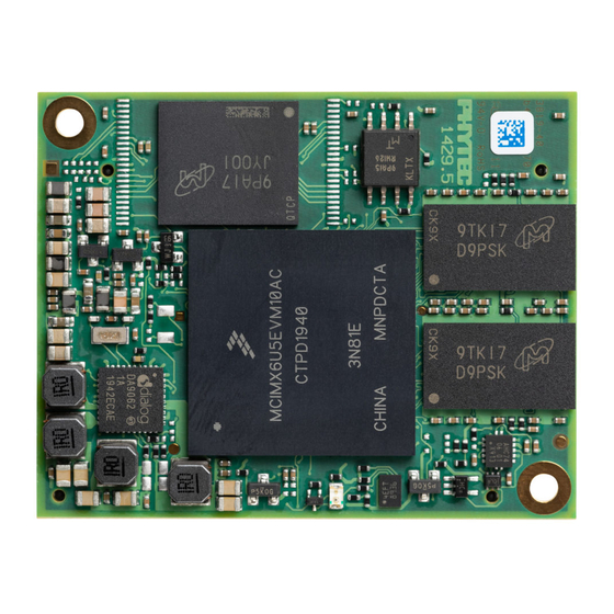
Page 18: Phycore-I.mx 6 Component Placement
R136 R146 R140 R122R116 R108 C313 C121 C310 C285 R139 R104 C110 C301 C216 C325 C238 C296 C321 C322 C308 C302 C219 R123 C292 C293 C298 Figure 2: phyCORE-i.MX 6 Component Placement (top view) © PHYTEC Messtechnik GmbH 2016 L-808e_2... -
Page 19: Figure 3: Phycore-I.mx 6 Component Placement (Bottom View)
C138 C184 C226 C189 C165 C130 C255 C123 C227 C252 C111 C159 C205 C122 C158 C256 C134 C166 C254 C251 C235 C215 C268 DMC2 C258 TP10 Figure 3: phyCORE-i.MX 6 Component Placement (bottom view) © PHYTEC Messtechnik GmbH 2016 L-808e_2... -
Page 20: Minimum Requirements To Operate The Phycore-I.mx 6
-i.MX 6 [PCM-058] Minimum Requirements to operate the phyCORE-i.MX 6 Basic operation of the phyCORE-i.MX 6 only requires supply of a +3.3 V input voltage with typical 2.5 A load and the corresponding GND connection. These supply pins are located at the phyCORE-Connector X1:... -
Page 21: Pin Description
Carrier Board/user target circuitry. The upper left-hand corner of the numbered matrix (pin X1C1) is thus covered with the corner of the phyCORE-i.MX 6. The numbering scheme is always in relation to the PCB as viewed from above, even if all connector contacts extend to the bottom of the module. -
Page 22: Figure 4: Pinout Of The Phycore-Connector (Top View)
Table • It is mandatory to avoid voltages at the IO pins of the phyCORE-i.MX 6 which are sourced from the supply voltage of peripheral devices attached to the SOM during power-up, or power–down. These voltages can cause a current flow into the controller especially if peripheral devices attached to the interfaces of the i.MX 6 are supposed to... - Page 23 (e.g. Camera_0). Thus, some signals might not be available on your module. • If the phyCORE-i.MX 6 is delivered with a carrier board (e.g. the phyBOARD-Mira) the pin muxing might be changed within the appropriate BSP in order to support all features of the carrier board.
- Page 24 VDD_3V3_LOGIC IPU2_CSI1 data 3 X_CSI1_DATA02 VDD_3V3_LOGIC IPU2_CSI1 data 2 X_CSI1_DATA_EN VDD_3V3_LOGIC IPU2_CSI1 data enable Ground 0 V Table 3: Pinout of the phyCORE-Connector X1, Row A connects to PMIC_VBBAT or VDD_MX6_SNVS via J3 (Table © PHYTEC Messtechnik GmbH 2016 L-808e_2...
-
Page 25: Table 3: Pinout Of The Phycore-Connector X1, Row A
VDD_3V3_LOGIC ENET transmit error X_ENET_RXD0 VDD_ENET_IO ENET RMII receive data 0 X_ENET_RXD1 VDD_ENET_IO ENET RMII receive data 1 X_ENET_RX_ER VDD_ENET_IO ENET RMII receive error Table 3: Pinout of the phyCORE-Connector X1, Row A (continued) © PHYTEC Messtechnik GmbH 2016 L-808e_2... -
Page 26: Table 4: Pinout Of The Phycore-Connector X1, Row B
VDD_3V3_LOGIC IPU2_CSI1 data 17 X_CSI1_DATA16 VDD_3V3_LOGIC IPU2_CSI1 data 16 Ground 0 V X_CSI1_DATA15 VDD_3V3_LOGIC IPU2_CSI1 data 15 X_CSI1_DATA14 VDD_3V3_LOGIC IPU2_CSI1 data 14 X_CSI1_PIXCLK VDD_3V3_LOGIC IPU2_CSI1 pixel clock Table 4: Pinout of the phyCORE-Connector X1, Row B © PHYTEC Messtechnik GmbH 2016 L-808e_2... - Page 27 Special care must be taken not to override the device configuration when using this pin as input (section 6.2). Special care must be taken not to override the device configuration when using this pin as input (section 6.2 ,section 10). © PHYTEC Messtechnik GmbH 2016 L-808e_2...
-
Page 28: Table 5: Pinout Of The Phycore-Connector X1, Row C
MIPI/CSI-2 data2+ X_CSI_D2M CSI2_I i.MX 6 internal MIPI/CSI-2 data2- X_CSI_CLK0P CSI2_I i.MX 6 internal MIPI/CSI-2 clock+ X_CSI_CLK0M CSI2_I i.MX 6 internal MIPI/CSI-2 clock- Ground 0 V Table 5: Pinout of the phyCORE-Connector X1, Row C © PHYTEC Messtechnik GmbH 2016 L-808e_2... - Page 29 6 internal LVDS1 clock- Ground 0 V X_LVDS1_TX0+ LVDS_O i.MX 6 internal LVDS1 data 0+ X_LVDS1_TX0- LVDS_O i.MX 6 internal LVDS1 data 0- Table 5: Pinout of the phyCORE-Connector X1, Row C (continued) © PHYTEC Messtechnik GmbH 2016 L-808e_2...
-
Page 30: Table 6: Pinout Of The Phycore-Connector X1, Row D
Ground 0 V Table 6: Pinout of the phyCORE-Connector X1, Row D Signal not used by any other interface can be used as GPIO without harming other features of the phyCORE-i.MX 6 (section 10). © PHYTEC Messtechnik GmbH 2016 L-808e_2... - Page 31 LVDS1 data 3- Tamper or ENET_RXC signal of X_TAMPER/ENET_RXC VDD_3V3_LOGIC i.MX 6 Pinout of the phyCORE-Connector X1, Row D (continued) Table 6: selection of either Tamper, or ENET_RXC signal can be done with jumper J6 (Table © PHYTEC Messtechnik GmbH 2016 L-808e_2...
-
Page 32: Jumpers
6 to your needs. It shows their default positions, and possible alternative positions and functions. A detailed description of each solder jumper can be found in the applicable chapter listed in the table. -
Page 33: Figure 6: Jumper Locations (Top View)
Jumpers Figure 6: Jumper Locations (top view) © PHYTEC Messtechnik GmbH 2016 L-808e_2... -
Page 34: Figure 7: Jumper Locations (Bottom View)
® phyCORE -i.MX 6 [PCM-058] Figure 7: Jumper Locations (bottom view) © PHYTEC Messtechnik GmbH 2016 L-808e_2... -
Page 35: Table 7: Jumper Settings
TAMPER signal of i.MX 6 is connected to phyCORE- 0 Ω (0402) Connector pin X1D70 ENET_RXC signal of i.MX 6 is connected to phyCORE- Connector pin X1D70 Table 7: Jumper Settings Default settings are in bold blue text © PHYTEC Messtechnik GmbH 2016 L-808e_2... -
Page 36: Power
X1 in detail. Primary System Power (VDD_3V3) The phyCORE-i.MX 6 operates off of a primary voltage supply with a nominal value of +3.3 V. On-board switching regulators generate the 2.5 V, 1.375 V, 1.5 V, 0.75 V, 1.2 V and 3 V voltage supplies required by the i.MX 6 MCU and on-board components from the... -
Page 37: Power Domains
NVCC_CSI, NVCC_EIM, NVCC_SD, NVCC_GPIO, (NVCC_ENET C EEPROM, SPI Flash, NAND Flash, eMMC, Ethernet PHY, User LED, reference output X1B5 NVCC_ENET is connected via jumper J1 and can alternatively be supplied by VDD_3V3_LOGIC (section 9.4.4) © PHYTEC Messtechnik GmbH 2016 L-808e_2... -
Page 38: Figure 8: Powering Scheme Of The Phycore- I.mx 6
® phyCORE -i.MX 6 [PCM-058] VDD_3V3 VDD_3V3_LOGIC Switch VDD_MX6_ARM VDD_MX6_SOC VDD_DDR3_1V5 DDR3_VREF Voltage divider VDD_ETH_1V2 DA9062 VDD_ETH_IO VDD_MX6_SNVS VDD_eMMC_1V8 VDD_MX6_HIGH Figure 8: Powering Scheme of the phyCORE- i.MX 6 © PHYTEC Messtechnik GmbH 2016 L-808e_2... -
Page 39: Supply Voltage For External Logic
If devices with a higher power consumption are to be connected to the phyCORE-i.MX 6 their supply voltage should be switched on and off by use of the X_3V3_GOOD signal. This way the power-up and power–down sequencing will be considered even if the devices are not supplied directly by VDD_3V3_LOGIC. -
Page 40: Reset
In case of a hard reset, no matter if it was triggered externally or internally, the PMIC holds down the nRESET signal until the module voltages are generated. The nRESET signal is released 2 ms after the last module voltage is generated correctly. © PHYTEC Messtechnik GmbH 2016 L-808e_2... -
Page 41: System Configuration And Booting
Internal Boot reserved Table 8: Boot Modes of the phyCORE-i.MX 6 The BOOT_MODE[1:0] lines have 10 kΩ pull-up and pull-down resistors populated on the module. Hence leaving the two pins unconnected sets the controller to boot mode 2, internal boot. -
Page 42: Boot Device Selection And Configuration
Please refer to the i.MX 6 Reference Manual for further information about the eFUSEs and the impact of the settings at the BCFG pins. For series production Phytec offers to order the phyCORE-i.MX 6 with a custom configuration of the eFUSEs © PHYTEC Messtechnik GmbH 2016 L-808e_2... -
Page 43: Table 9: Boot Configuration Pins At The Phycore-Connector
X1A24 X_ECSPI1_SS0 3.3 V eCSPI1 chip select 0 BCFG4[7] X1A20 X_UART3_RTS_B 3.3 V UART3 request to send input Table 9: Boot Configuration Pins at the phyCORE-Connector Connected to GND for the standard module configuration © PHYTEC Messtechnik GmbH 2016 L-808e_2... -
Page 44: System Memory
6 controller. Refer to the i.MX 6 Reference Manual for accessing and configuring these registers. The maximum memory size listed is as of the printing of this manual. Please contact PHYTEC for more information about additional, or new module configurations available. -
Page 45: Nand Flash Memory (U12)
System Memory NAND Flash Memory (U12) Use of Flash as non-volatile memory on the phyCORE-i.MX 6 provides an easily reprogrammable means of code storage. The NAND Flash memory at U12 is connected to the General Purpose Media Interface (GPMI). Dependent on the memory size one or more of the chip enable signals NANDF_CS0, NANDF_CS1, NANDF_CS2 and NANDF_CS3 of the GPMI interface select the NAND Flash. -
Page 46: Spi Flash Memory (U9) )
EEPROM write protection states via J4 SPI Flash Memory (U9) ) The SPI Flash Memory of the phyCORE-i.MX 6 at U9 can be used to store configuration data or any other general purpose data. Beside this it can also be used as boot device recovery boot device . -
Page 47: Sd / Mm Card Interfaces
SD / MMC Card Interfaces SD / MM Card Interfaces The phyCORE bus features two SD / MM Card interface. On the phyCORE-i.MX 6 the interface signals extend from the controllers third and first Ultra Secured Digital (uSDHC3 / uSDHC1) Host Controller to the phyCORE-Connector. -
Page 48: Serial Interfaces
Universal Asynchronous Interface The phyCORE-i.MX 6 provides two high speed universal asynchronous interfaces with up to 4 MHz and one with additional hardware flow control (RTS and CTS signals). The following table shows the location of the signals on the phyCORE-Connector. -
Page 49: Usb Otg Interface
Serial Interfaces USB OTG Interface The phyCORE-i.MX 6 provides a high speed USB OTG interface which uses the i.MX 6 embedded HS USB OTG PHY. An external USB Standard-A (for USB host), USB Standard-B (for USB device), or USB mini-AB (for USB OTG) connector is all that is needed to interface the phyCORE-i.MX 6 USB OTG functionality. -
Page 50: Ethernet Interface
-i.MX 6 [PCM-058] Ethernet Interface Connection of the phyCORE-i.MX 6 to the world wide web or a local area network (LAN) is possible using the on-board GbE PHY at U2. It is connected to the RGMII interface of the i.MX 6. The PHY operates with a data transmission speed of 10 Mbit/s, 100 Mbit/s or 1000 Mbit/s. -
Page 51: Software Reset Of The Ethernet Controller
In order to guarantee that the MAC address is unique, all addresses are managed in a central location. PHYTEC has acquired a pool of MAC addresses. The MAC address of the phyCORE-i.MX 6 is located on the bar code sticker attached to the module. This number is a 12-digit HEX value. -
Page 52: Rmii Interface
ENET RMII RX enable X1B67 X_ENET_TX_EN VDD_ENET_IO ENET RMII TX enable X1B69 X_ENET_TXD0 VDD_ENET_IO ENET RMII transmit data 0 X1B70 X_ENET_TXD1 VDD_ENET_IO ENET RMII transmit data 1 Table 16: Location of the RMII Interface Signals © PHYTEC Messtechnik GmbH 2016 L-808e_2... -
Page 53: Spi Interface
The SPI Flash is accessed through SS1 of module eCSPI1 (section 7.5). Special care must be taken not to override the device configuration when using this pin as input (section 6.2). © PHYTEC Messtechnik GmbH 2016 L-808e_2... -
Page 54: I 2 C Interface
S) and Intel AC’97 standard. The i.MX 6 provides three instances of the SSI module. On the phyCORE-i.MX 6 SSI is brought out to the phyCORE-Connector through port 5 of the i.MX 6's Digital Audio Multiplexer (AUDMUX5). The main purpose of this interface is to connect to an external codec, such as I S. -
Page 55: Can Interface
CAN Interface Signal Location SATA Interface The SATA II interface of the phyCORE-i.MX 6 is a high-speed serialized ATA data link interface compliant with SATA Revision 3.0 (physical layer complies with SATA Revision 2.5) which supports data rates of up to 3.0 Gbit/s. The interface includes an internal DMA engine, command layer, transport layer, link layer and the physical layer. -
Page 56: Pci Express Interface
-i.MX 6 [PCM-058] 9.10 PCI Express Interface The 1-lane PCI Express interface of the phyCORE-i.MX 6 provides PCIe Gen. 2.0 functionality which supports 5 Gbit/s operation. Furthermore the interface is fully backwards compatible to the 2.5 Gbit/s Gen. 1.1 specification. Additional control signals which might be required (e.g. -
Page 57: General Purpose I/Os
X1B27 (EIM_DA15) and X1B44 (EIM_EB1) are latched during boot to determine the device configuration (section 5). Because of that special care must be taken not to override the device configuration when using these pins as input. To avoid this danger, the eFUSEs can be used. © PHYTEC Messtechnik GmbH 2016 L-808e_2... -
Page 58: User Led
-i.MX 6 [PCM-058] 11 User LED The phyCORE-i.MX 6 provides one green user LED (D1) on board. It can be controlled by setting GPIO1_04 to the desired output level. A high-level turns the LED on, a low-level turns it off. -
Page 59: Debug Interface
Debug Interfaces 12 Debug Interface The phyCORE-i.MX 6 is equipped with a JTAG interface for downloading program code into the external flash, internal controller RAM or for debugging programs currently executing. Table 24 shows the location of the JTAG pins on the phyCORE-Connector X1. -
Page 60: Display Interfaces
The signals from the LCD interface of the i.MX 6 are brought out at the phyCORE-Connector X1. Thus an LCD interface with up to 24-bit bus width can be connected directly to the phyCORE-i.MX 6. The table below shows the location of the applicable interface signals. Pin #... -
Page 61: Lvds Display Interface
The LVDS-Signals from both channels of the on-chip LVDS Display Bridge (LDB) on the i.MX 6 are brought out at phyCORE-Connector X1. Thus up to two LVDS-Displays can be connected directly to the phyCORE-i.MX 6. The location of the applicable interface signals can be found in the table below. -
Page 62: High-Definition Multimedia Interface (Hdmi)
As the signals extend directly from the i.MX 6's HDMI PHY a standard HDMI connector, a 5 V level shifter for the DDC and the CEC signals and an optional ESD circuit protection device is all that is needed to interface the phyCORE-i.MX 6's HDMI functionality. © PHYTEC Messtechnik GmbH 2016 L-808e_2... -
Page 63: Camera Interfaces
LVDS Camera Interface 15 Camera Interfaces The phyCORE-i.MX 6 SOM offers various interfaces to connect digital cameras. Up to two parallel camera interfaces (IPU1_CSI0 and IPU2_CSI1 ) as well as the interface to the MIPI/CSI-2 Host Controller are supported and brought out in different ways. All signals... -
Page 64: Figure 12: Camera Interfaces At The Phycore-Connector (Parallel 0(Csi0 Of Ipu#1)
Camera Interfaces at the phyCORE-Connector (Parallel 0(CSI0 of IPU#1), Parallel 1(CSI1 of IPU#2), and MIPI/CSI-2) The camera interfaces of the phyCORE-i.MX 6 include all signals and are prepared to be used as phyCAM-S(+), phyCAM-P, or MIPI/CSI-2 interface on an appropriate carrier board. -
Page 65: Parallel 0 Camera Interface (Csi0 Of Ipu#1)
Recommended to implement special control features for the camera interface circuitry on the carrier board (e.g. enabling/disabling of the interface, switching between phyCAM-P and phyCAM-S, etc.). Please refer to L-748 or appropriate Phytec CB designs as reference. © PHYTEC Messtechnik GmbH 2016 L-808e_2... -
Page 66: Parallel 1 Camera Interface (Csi1 Of Ipu#2)
Recommended to implement special control features for the camera interface circuitry on the carrier board (e.g. enabling/disabling of the interface, switching between phyCAM-P and phyCAM-S, etc.). Please refer to L-748 or appropriate Phytec CB designs as reference. © PHYTEC Messtechnik GmbH 2016 L-808e_2... -
Page 67: Mipi/Csi-2 Camera Interface
CCM clock output 1 (Camera0 X1D16 X_CCM_CLKO1 O VDD_3V3_LOGIC MCLK) Table 31: Camera Interface MIPI/CSI-2 Signal Location Use of the I²C bus and the camera clock signal allows to directly connect a MIPI/CSI-2 camera module. © PHYTEC Messtechnik GmbH 2016 L-808e_2... -
Page 68: Utilizing The Camera Interfaces On A Carrier Board
-i.MX 6 [PCM-058] 15.4 Utilizing the Camera Interfaces on a Carrier Board On Phytec carrier boards the interfaces are used directly as parallel interface according to the phyCAM-P standard (Figure 13) and/or by converting the signals with an LVDS... -
Page 69: Tamper Detection
Tamper Detection 16 Tamper Detection The phyCORE-i.MX 6 supports the tamper detection feature of the i.MX 6. With the tamper detection feature it is possible to recognize when the device encounters unauthorized opening, or tampering. For this purpose, the i.MX 6's Tamper Detection signal is available at pin X1D70 of the phyCORE-Connector. -
Page 70: Technical Specifications
6 D2.6mm Figure 15: Physical Dimensions (top view) The physical dimensions of the phyCORE-i.MX 6 are represented in Figure 15. The module’s profile is max. 10 mm thick, with a maximum component height of 3.0 mm on the bottom (connector) side of the PCB and approximately 5.0 mm on the top (microcontroller) side. -
Page 71: Table 32: Technical Specifications
Technical Specifications Note: To facilitate the integration of the phyCORE-i.MX 6 into your design, the footprint of the phyCORE-i.MX 6 is available for download (section 18.1). Additional specifications: Dimensions: 40 mm x 50 mm Weight: approx. 17.4 g Storage temperature: -40 °C to +125 °C... -
Page 72: Product Temperature Grades
-20 °C to +105 °C -40 °C to +95 °C -40 °C to +85 °C Consumer Consumer Commercial 0 °C to +95 °C 0 °C to +95 °C 0 °C to +70 °C Table 33: Product Temperature Grades © PHYTEC Messtechnik GmbH 2016 L-808e_2... -
Page 73: Connectors On The Phycore-I.mx 6
Technical Specifications 17.2 Connectors on the phyCORE-i.MX 6: Manufacturer Samtec phyCORE-Connector X1: Number of pins per contact rows 140 pins (2 rows of 70 pins each) Samtec part number (lead free) BSH-070-01-L-D-A-K-TR (old part#) REF-183456-03 Information on the receptacle sockets that correspond to the connectors populating the underside of the phyCORE—i.MX 6 is provided below. -
Page 74: Hints For Integrating And Handling The Phycore-I.mx 6
It is available in different file formats. Use of this data data as shown in Figure 16. allows to integrate the phyCORE-i.MX 6 SOM as a single component into your design. different support packages are available to support you in all stages of your embedded development. Please visit http://www.phytec.de/de/support/support-... -
Page 75: Figure 16: Footprint Of The Phycore-I.mx 6
A tolerance of +/- 0.1 mm applies to all indicated measures, except for the measures of the outer edges which have a tolerance of +/- 0.2 mm Figure 16: Footprint of the phyCORE-i.MX 6 © PHYTEC Messtechnik GmbH 2016 L-808e_2... -
Page 76: Handling The Phycore-I.mx 6
® phyCORE -i.MX 6 [PCM-058] 18.2 Handling the phyCORE-i.MX 6 • Modifications on the phyCORE Module Removal of various components, such as the microcontroller and the standard quartz, is not advisable given the compact nature of the module. Should this nonetheless be necessary, please ensure that the board as well as surrounding components and sockets remain undamaged while de-soldering. -
Page 77: Revision History
19 Revision History Date Version Changes in this manual numbers 04.06.2015 Manual First edition. L-808e_1 Describes the phyCORE-i.MX 6 PCB-Version 1429.1 04.08.2016 Manual Second edition. L-808e_2 Describes the phyCORE-i.MX 6 PCB-Version 1429.2 and 1429.3 © PHYTEC Messtechnik GmbH 2016 L-808e_2... - Page 78 ® phyCORE -i.MX 6 [PCM-058] © PHYTEC Messtechnik GmbH 2016 L-808e_2...
-
Page 79: Index
X1-B..........12 X1-C ..........14 X1-D..........16 General Purpose I/Os......43 PMIC ..........22 GND Connection ........62 PMIC_VBAT......... 25 Power Consumption ......57 Humidity..........57 Power Domains ........23 Power Management IC ......22 © PHYTEC Messtechnik GmbH 2016 L-808e_2... - Page 80 System Configuration ......27 System Memory ........30 VDD_3V3..........22 System Power........22 VDD_DDR3_1V5 ........23 VDD_eMMC_1V8 ........23 VDD_MX6_SNVS........25 Tamper Detection ........ 55 Voltage Output ........25 Technical Specifications ......56 Weight..........57 U11........... 31 © PHYTEC Messtechnik GmbH 2016 L-808e_2...
- Page 81 How would you improve this manual? Did you find any mistakes in this manual? page Submitted by: Customer number Name: Company: Address: Return to: PHYTEC Messtechnik GmbH Postfach 100403 D-55135 Mainz, Germany Fax : +49 (6131) 9221-33 © PHYTEC Messtechnik GmbH 2016 L-808e_2...
- Page 82 Published by © PHYTEC Messtechnik GmbH 2016 Ordering No. L-808e_2 Printed in Germany...
Need help?
Do you have a question about the phyCORE-i.MX 6 and is the answer not in the manual?
Questions and answers