Table of Contents
Advertisement
This product is a lead free model.
Lead free solder is used in PWB stamped LF mark.
Please keep the following conditions when you repair.
1. Use lead free solder.
* Koki's lead free solder S3X-55M 0.6mm
(CLARION Parts No.642-0231-01)
* Koki's lead free solder S3X-55M 1.0mm
(CLARION Parts No.642-0231-02)
2. Use a nitrogen solder system.
3. Do not use "General solder" and "Lead free solder"
together.
NOTES
*
The tuner of this unit is DSP type. When you exchange
the tuner pack(880-2091D), it is necessary to adjust for
S-meter etc. The special JIG is used for an accurate
adjustment.
*
This DVD video player can play the following discs.
DVD video discs
Video CDs
Audio CDs
MP3 ID3 TAG
*
Precautions when creating an MP3 disc
When writing an MP3/WMA file on a disc, please select
"ISO9660 level 1 or level 2(without including expansion
format)" as the writing software format. Normal playback
may not be possible if the disc is recorded on another
format.
Clarion Co., Ltd.
50 Kamitoda, Toda-shi, Saitama 335-8511 Japan
Service Dept.: 5-66 Azuma , Kitamoto-shi, Saitama 364-0007 Japan
Tel: +81-48-541-2335 / 2432 FAX: +81-48-541-2703
Service Manual
MONI
CD TEXT
WMA
- 1 -
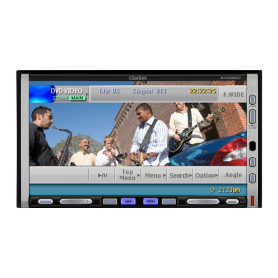
DVD Multimedia Station
With Touch Panel Control
Model
(QZ-6070E-B)
In case of a track recorded at VBR (variable bit rate), the
display for the play time of the track may be slightly dif-
ferent from the actual play time. Also, the recommended
value of VBR ranges from 64 kbps to 320kbps.
*
Manufactured under license from Dolby Laboratories.
"Dolby" and the double-D symbol are trademarks of Dolby
Laboratories.
*
"DTS" and "DTS Digital Out" are registered trademarks
of Digital Theater Systems, Inc.
*
This product includes technology owned by Microsoft
Corporation and cannot be used or distributed without a
license from MSLGP.
*
and
or registered trademarks of Microsoft Corporation in the
United States and/or other countries.
*
is for legal or rightholder-authorized copying only.
Don't steal music.
iPod is a trademark of Apple Computer, Inc., registered
in the U.S. and other countries.
*
This product incorporates copyright protection technol-
ogy that is protected by U.S. patents and other intellec-
tual property rights.
Use of this copyright protection technology must be au-
thorized by Macrovision, and is intended for home and
other limited viewing uses only unless otherwise autho-
rized by Macrovision. Reverse engineering or disas-
sembly is prohibited.
*
We cannot supply PWB with component parts in
principle. When a circuit on PWB has failure, please
repair it by component parts base.
Parts which are not mentioned in service manual are
not supplied.
*
Specifications and design are subject to change without
notice for further improvement.
Published by Service Dept.
298-6379-00 Sep.2006
Printed in Japan
logo are trademarks
MAX668RVD
Advertisement
Table of Contents

Related Manuals for Clarion MAX668RVD


Summary of Contents for Clarion MAX668RVD
- Page 1 Clarion Co., Ltd. Published by Service Dept. 50 Kamitoda, Toda-shi, Saitama 335-8511 Japan 298-6379-00 Sep.2006 Service Dept.: 5-66 Azuma , Kitamoto-shi, Saitama 364-0007 Japan Printed in Japan Tel: +81-48-541-2335 / 2432 FAX: +81-48-541-2703 Service Manual DVD Multimedia Station With Touch Panel Control...
-
Page 2: Specifications
Power source voltage: 14.4V DC (10.8 to 15.6V allowable) Ground: Negative Current consumption: 4.0A(at 1W) Dimensions(mm): Main unit; 178(W)x100(H)x160.0(D) Remote Control Unit; 54(W)x28.8(H)x155(D) Weight: Main Unit; 2.4kg Remote Control Unit; 100g (including battery) Top view of the unit MAX668RVD - 2 -... - Page 3 Also take care not to apply the tip with force. 9. Turn the unit OFF during disassembly and parts replacement. Recheck all work before you apply power to the unit. MAX668RVD - 3 -...
- Page 4 1. Adjust VR702 so that the black-white level of the wave- form of TP716(G) will become 3.8V+0.1/-0.1V. Black Withe 3.8V+0.1/0.1V Withe Black White balance pre-adjustment Measurement conditions: the same conditions as the ad- justment of "Power supply voltage". / Measuring instrument: oscilloscope(DC range) MAX668RVD - 4 -...
-
Page 5: Error Display
If an error display other than the ones described above appears, press the [RESET] button. RESET button When the [RESET] button is pressed, frequencies of TV/radio stations, titles, etc. stored in memory are cleared. MAX668RVD - 5 -... -
Page 6: Wire Connection
FRONT R-CH(-) GRY/BLK N.C. REAR R-CH(+) iPod Connector REAR R-CH(-) PUR/BLK BACK UP(15A) AUDIO-L GRN/BLK REAR L-CH(-) AUDIO-R A RETURN PHONE MUTE ACC IDENT ACC DET N.C. IPOD-AV BLU/WHT AMP-REM AV-IPOD ORN/WHT D/FW GND 3.3V L.GRN F/W-PWR MAX668RVD - 6 -... - Page 7 : O : The illumination ON signal output. pin 52: NU : IN : Not in use. pin108: BLINK LED : O : Signal output for the LED. pin 53: IRI : IN : The remote control signal input. MAX668RVD - 7 -...
-
Page 8: Table Of Contents
Rear V Sel 2 ( pin 131 ) 716-3504-10 SCREW(M2.6x4) Rear V Sel 3 ( pin 128 ) 714-2610-8B MACHINE SCREW(M2.6x10) Rear V Sel 4 ( pin 127 ) 716-3504-20 SCREW(M2.6x4) 716-1886-00 DECORATIVE SCREW(M2x3.4) 746-0935-00 WASHER 276-0111-00 SETPLATE MAX668RVD - 8 -... - Page 9 18 17 15 43 36 41 3 32 MAX668RVD - 9 -...
- Page 10 LCD PWB 780-2003-03 SCREW(M2x3) 347-8068-00 DOUBLE FACE 039-2808-05 FPC 347-8069-00 DOUBLE FACE 335-7846-00 IR-FILTER 347-8070-00 DOUBLE FACE 382-7966-00 BUTTON(PWR) 347-8072-00 FILM 382-7967-00 BUTTON(OP/CL) 347-8078-00 EARTH FILM 382-7968-01 BUTTON(TA) 347-8084-00 FILM 382-7969-00 BUTTON(ADJ) 331-3672-11 SHIELD CASE 382-7970-00 BUTTON(PLAY) MAX668RVD - 10 -...
- Page 11 168-1042-78 16V 0.1uF C166 168-1042-78 16V 0.1uF C254 166-2701-50 27pF CH C341 168-1032-55 0.01uF K C167 163-1073-15 6.3V 100uF C256 163-2263-15 6.3V 22uF C350 166-1021-50 1000pF CH C168 168-3322-55 3300pF K C258 043-0264-56 270pF C351 168-1042-78 16V 0.1uF MAX668RVD - 11 -...
- Page 12 119-2231-15 1/10W 22k ohm R224 119-1831-15 1/10W 18k ohm L113 010-3105-62 1k ohm/100MHz R134 119-1031-15 1/10W 10k ohm R225 119-1031-15 1/10W 10k ohm L201 010-3103-64 1.5k ohm/100MHz R135 119-2231-15 1/10W 22k ohm R226 119-1031-15 1/10W 10k ohm MAX668RVD - 12 -...
-
Page 13: Main Pwb
166-1011-50 100pF CH C414 042-0592-58 16V 10uF C431 042-0472-91 16V 47uF C447 166-1011-50 100pF CH C415 163-1053-65 50V 1uF C432 168-1042-78 16V 0.1uF C448 168-1045-56 0.1uF Z C416 178-4742-78 0.47uF C433 178-3342-78 0.33uF C449 166-1011-50 100pF CH MAX668RVD - 13 -... - Page 14 CCT612 050-0140-63 1/32W 47k ohm x4J UEN-A C618 168-1042-78 16V 0.1uF CCT613 050-0140-63 1/32W 47k ohm x4J IC501 051-5440-08 S-80931CNMC-G81 C619 168-1042-78 16V 0.1uF D400 001-0517-90 1SS355 IC502 051-3406-90 NJM2078M C620 168-1042-78 16V 0.1uF D401 001-0517-90 1SS355 IC503 051-5410-38 BU4820G-TR MAX668RVD - 14 -...
- Page 15 119-3321-15 1/10W 3.3k ohm R530 119-1041-15 1/10W 100k ohm Q425 198-0302-50 2SK302 Y,GR R449 119-1031-15 1/10W 10k ohm R531 119-1051-15 1/10W 1M ohm Q426 125-2026-95 UN521N R450 119-4711-15 1/10W 470 ohm R532 032-0140-67 1/10W 3.3k ohm F MAX668RVD - 15 -...
- Page 16 C732 168-1032-55 0.01uF K C772 166-3301-50 33pF CH C812 166-4711-50 470pF CH C733 168-1032-55 0.01uF K C773 168-1042-78 16V 0.1uF C814 166-4711-50 470pF CH C734 168-4732-78 0.047uF K C774 166-3301-50 33pF CH C816 168-1042-78 16V 0.1uF MAX668RVD - 16 -...
- Page 17 R707 119-1001-15 1/10W 10 ohm R782 119-1051-15 1/10W 1M ohm D901 001-0517-90 1SS355 R708 119-1011-15 1/10W 100 ohm R783 119-2711-15 1/10W 270 ohm D902 001-0517-90 1SS355 R709 119-9121-15 1/10W 9.1k ohm R784 119-2421-15 1/10W 2.4k ohm MAX668RVD - 17 -...
- Page 18 119-4711-15 1/10W 470 ohm S1012 013-6312-50 SKRP-ABE-010 D1012 001-7098-90 CL-190UB2C-X-T R1007 119-3311-15 1/10W 330 ohm S1013 013-6312-50 SKRP-ABE-010 D1013 001-7098-90 CL-190UB2C-X-T R1008 119-3311-15 1/10W 330 ohm 039-2902-00 PWB(WITHOUT D1014 001-7098-90 CL-190UB2C-X-T R1009 119-0000-05 1/10W 0 ohm JW COMPONENTS) MAX668RVD - 18 -...
-
Page 19: Tuner Pwb
REG. Ce-NET CONECTOR TO AUDIO BLOCK AND TUNER P400 (13P) IC403 Q425 Q408 REM3.3V IC402 DRIVER AV8.5V B/U3.3V 3.3V REG. REG. MEM3.3V TO DVD MECHANISM IC461 IC460 IC462 Q463 SW&9V 1.8V 3.3V REM5V REGURATER REG. REG. - 19 - MAX668RVD... -
Page 20: Ant-Recept
ANT Recept. Remote cont. V-IN terminal N.C. N.C. V-GND N.C. J303 C125 To P1103 of Joint PWB-A (Page 25) C124 R126 R124 Tuner PWB (B1) *Four layers To J1100 of Joint PWB-B (Page 25) COMPONENT SIDE MAX668RVD - 20 -... - Page 21 C350 5.1V 1000p 4.8V 5.0V 1.9V C364 0.8V 0.047 R361 R366 Q350 2SA1586 C363 AV5V 3.3V C361 100 16V LZ C359 1.0 B C358 16V 470 Tuner PWB (B1) *Four layers C357 10 25V SOLDER SIDE - 21 - MAX668RVD...
- Page 22 IC105 BA033CC0FP L113 3.3V S-GND (3.3V-DIG) R179 mmZ1608S102CT mmZ1608S102CT 3.3V C1101 IC102 To 4/4 HA17558AF 0.018 (3.3V-ANA) L112 REM5V 1/2VCC mmZ1608S102CT MICOM To 3/4 4.7V 4.7V -GND VREF 8.5V 4.7V To 4/4 SPDIF SPDIF SPD-G SPDIF-G MAX668RVD - 22 -...
- Page 23 Q209 2-ZONE 2-ZONE MUTE R277 DTA143ZUA MUTE:2.8V MUTE:2.8V SUB-MUTE Q208 2SD1306 R249 C275 C239 R281 SYS-MUTE: R246 R247 6.3V 6.3V 1.7V DTA143ZUA SUB-R SYS-MUTE:1.8V SYS-MUTE R250 L214 R280 C242 680p To 4/4 8.6V AV8.5V MICOM-GND F-GND MAX668RVD - 23 -...
- Page 24 C338 B/U14V Jack R312 10 16V DC-GND 5.0V Video Line-IN REM-5V TP353 F-SEL DVD A/C D312 DAN217U P302 VIDEO-IN To 2/4 V-GND REM5V DVD-A/C AV8.5V V-GND VISUAL1 To 3/4 F-GND V-GND V-GND V-OUT V-OUT-G AV8.5V S-GND MAX668RVD - 24 -...
- Page 25 3.0V SEL-2 SEL-2 9.8V 9.8V MTR10V 3.3V F-SEL F-SEL REM5V 4.9V REM-5V REM-5V 4.8V MOT1R MOT1F 4.9V REM-5V REM-5V 4.8V 3.1V PULSE OP/CL DC-GND DC-GND DC-GND DC-GND 13.7V B/U14V B/U14V 13.7V B/U14V B/U14V 3.2V AV-ON AV-ON MAX668RVD - 25 -...
- Page 26 N.C. R(+) REAR-R(-) N.C. F/W-PWR J670 10 9 8 To FAN Motor C422 To J1100 of Joint PWB-A (Page 25) R415 IC672 Main PWB (B3) *Four layers To J1101 of Joint PWB-B COMPONENT SIDE (Page 25) MAX668RVD - 26 -...
-
Page 27: Dvd Mech
To CN701 of DVD mech(30P) FPC(039-2706-05) To CN401 of DVD mech(12P) D500 R550 R555 Q504 R562 Q505 D674 Main PWB (B3) *Four layers To P1101 of Joint PWB-C SOLDER SIDE (Page 25) FPC(039-2808-05) To J700 of LCD PWB (Page 37) MAX668RVD - 27 -... - Page 28 AUDIO L 1.6V IC403 IPOD-L R492 3.1V R454 IPOD-AV To 2/6 HA12187FP ACC IDENT SYS-ACC AV-IPOD 3.1V Q432 9 10 UN5212 3.1V 3.1V CENET-RX R493 R456 CENET-TX R494 3.1V 3.1V To 2/6 IPOD-ON IPOD-DET AV-IPOD R458 IPOD-AV MAX668RVD - 28 -...
- Page 29 3.2V W-IR B/U14V (VDD3.3V) (VDD3.3V) (REM3.3V) (REM3.3V) R549 DVD-IND 100K RESET DVD-EJ IC504 BR93L56F-W To 5/6 V2/5 3.3V 3.3V POWER 3.2V Q505 OP/CL UN5211 M108 MECH 3.3V BL-LED Q504 2SA1576A SCLK SCLK R557 IC505 BR93L56F-W TP468 MAX668RVD - 29 -...
- Page 30 5.0V 5.0V 3.1V R659 1R/1C R626 IC603 To 2/6 SN74AHC2G53 4.9V ROM-EN 1CLR 5.0V C617 2200p C616 R624 2200p 2CLR R625 5.0V 5.0V 5.0V R627 5.0V 3.1V 5.0V 2R/2C 2:INH 1:COM(OUT) 6:Y1:DELAY 5.0V IC604 SN74AHC1G32 7:Y0:NORMAL MAX668RVD - 30 -...
- Page 31 2.1V 2.0V C693 2.1V 2.1V C698 2.2V 2.1V C699 C700 1.9V 4.9V C701 C703 1.9V 1.9V C702 To 5/6 R688 TP663 1.3V TP664 0.4V 1.9V C704 C705 1.9V R689 1.4V TP665 C706 1.5V 1.9V R690 TP666 - 31 - MAX668RVD...
- Page 32 To 2/6 L465 DVD+5V SUB-MUT SYNC 4.9V SYNC DVD+5V INES-ON To 4/6 9V REG R479 3.3V DVD+3.3V L466 3.3V DVD+3.3V L467 1.8V L468 DVD+1.8V 1.8V DVD+1.8V 9.0V DVD+9V L469 9.0V DVD+9V To CN401 of DVD mech MAX668RVD - 32 -...
- Page 33 VIDEO R746 6.8K ILL+9V R710 X701 ILL-GND 5.6K 3.579545MHz REM+5V C755 D-GND Q705 TP704 R719 UM5211 BRIGHT Q701 Q703 39K (F) UM5211 UM5211 C754 V-MUTE X700 4.433618M Q706 COLOR 2SA1738 CLAMP R747 1.5K L:VTR/DVD TP700 H:TV/RGB MAX668RVD - 33 -...
- Page 34 C776 1000p D711 R766 1SS355 1.8K R782 C769 560p TP46 TP45 R781 C770 R779 C787 2.6V 5.2V 220p Q712 R786 L712 C779 R778 2SC4081 3.3u 1000p 2.6V 2.6V C778 100p IC710 NJM2107F R784 R785 2.4K 4.7K - 34 - MAX668RVD...
- Page 35 R819 MOD W J805 VIDEO/RGB IC801-8 4.9V 9.2V ILL+9V ILL-GND 3.5V D802 1SS355 POWER 3.5V IC801- IC801-10 OP/CL 15,17,19,23 4.2V D-GND 4.8V 3.8V 0.4V 4.9V REM+5V CCT801 1Kx4 R812 4.8V KI-3 KO-0 K0-1 9.2V ILL+9V ILL-GND MAX668RVD - 35 -...
- Page 36 POWER 13.4V 0.6V R903 L903 0.6V 0.5V 100uH TM804 R905 680K 5.3V EARTH PLATE 2.5V 0.5V +5.3V C905 2200p 5.3V-ADJ D902 L902 1SS355 100uH 7.4V VR600 +7.5V D901 L901 1SS355 100uH 15.1V +15.0V TM801 EARTH PLATE MAX668RVD - 36 -...
- Page 37 (Page 38) TP705 VR701 TP713 TP711 TP709 TP710 To J460 of Main PWB F900 (Page 27) R989 C960 D961 R964 R966 VR600 D965 P950 LCD PWB (B4) LCD PWB (B4) To LCD SOLDER SIDE COMPONENT SIDE MAX668RVD - 37 -...
- Page 38 9.2V ILL+9V KI-2 4.8V 4.8V KI-1 S1005 S1009 S1012 KO-0 >> VOL- KO-1 KO-2 S1006 S1010 S1013 KO-3 4.8V K1-0 << VOICE 9.2V ILL+9V ILL-GND D-GND Switch PWB-B (B5) Switch PWB-B (B5) SOLDER SIDE COMPONENT SIDE MAX668RVD - 38 -...
- Page 39 Clarion Co., Ltd. Published by Service Dept. 50 Kamitoda, Toda-shi, Saitama 335-8511 Japan Service Dept.: 5-66 Azuma , Kitamoto-shi, Saitama 364-0007 Japan Printed in Japan Tel: +81-48-541-2335 / 2432 FAX: +81-48-541-2703 Service Manual DVD mechanism 929-2506-00 Model NOTES 658-0244-01 C0JBAZ001014...
- Page 40 pin 10: A out R+ : O : Audio signal right channel positive output. output buffers are placed in a High-Z state during a READ cycle. DQM 0 corresponds pin 11: A out L- : O : Audio signal left channel negative output. to D0-D7.
- Page 41 pin 74: D 8 :I/O: Data input/output. 658-0246-11 C3GBCA000001 16Kb FRAM (FM25C160-GTR) pin 75: VDD : - : Positive supply voltage. pin 76: D 9 :I/O: Data input/output. Terminal Description pin 77: D 10 :I/O: Data input/output. 1: CS IN : IN : The chip select command input.
- Page 42 pin 52: MD22 :I/O: SDRAM data bus (1V) pin118: CVBS/C : O : Composite/S-Video Chrominance (0.5V) pin 53: VDDIO : - : I/O pad power (3.3V) pin119: RSET : O : Current setting resistor connection (1.4V) pin 54: MD23 :I/O: SDRAM data bus (0V) pin120: COMP : O : Compensation capacitor connection (2V) pin 55: MD24...
- Page 43 pin186: LA2 : O : Latch address (3.3V) pin187: LA3 : O : Latch address (3.3V) pin188: VSSIO : - : I/O pad ground (0V) pin189: RD : O : Read signal (3.3V) pin190: LHLDA : - : Not used pin191: LHLD : - : Not used pin192: VDD...
- Page 44 Remove SUSPENSION-ASSY DISASSEMBLY 1. Remove EARTH-SPRING and OFFSET-SPRINGS. Remove Servo-PWB Earth-Spring 1. Solder two points of FPC to prevent destruction with static electricity. Offset-Spring Servo PWB side Solder points Pick-up side Offset-Spring Suspension-ASSY 2. Remove FCPs from PICK-UP-UNIT and SENSOR-FPC- ASSY.
- Page 45 [NOTE] Remove LOADING-GEAR/LOADING-MOTOR When assembling, set the dot marks of LOCK-GEAR(1) 1. Remove six LOADING-GEARS in the following order. and MAIN-CHASSIS. (1) > (4) > (3) > (2) > (5) > (6) 2. Remove two SCREWS,and remove LOADING-MOTOR- ASSY. Loading-Motor-ASSY Loading-Gear(1) Gear(1) Loading-Gear(6)
-
Page 46: Upper Chassis
EXPLODED VIEW / PARTS LIST GREASE GREASE GREASE GREASE GREASE GREASE GREASE GREASE GREASE : MOLYKOTE PG-641 PART NO. DESCRIPTION Q'TY PART NO. DESCRIPTION Q'TY ----------- Servo PWB 658-0238-03 Laoding Gear (6) 658-0247-01 Suspension Assy 658-0238-04 Worm Gear Housing Spring 658-0244-16 Upper Chassis 658-0238-05 Clamp Rack 658-0247-02 Sensor FPC Assy... -
Page 47: Electrical Parts List
ELECTRICAL PARTS LIST Servo PWB(BM1) section REF No. PART No. DESCRIPTION REF No. PART No. DESCRIPTION REF No. PART No. DESCRIPTION C101 658-0246-12 50V560pF C253 658-0240-12 0.1uF 10WV C544 658-0240-12 0.1uF 10WV C102 658-0240-12 0.1uF 10WV C261 658-0240-12 0.1uF 10WV C545 658-0240-12 0.1uF 10WV C103... - Page 48 REF No. PART No. DESCRIPTION REF No. PART No. DESCRIPTION REF No. PART No. DESCRIPTION L403 658-0240-32 YELTBMHS800T R223 033-3931-15 1/16W 39k ohm R431 658-0240-23 100k ohm 1/16W L404 658-0240-32 YELTBMHS800T R227 033-0000-05 1/16W 0 ohm R441 033-4731-15 1/16W 47k ohm L406 658-0240-32 YELTBMHS800T R231...
-
Page 49: Block Diagram
BLOCK DIAGRAM IC101 RF AMP CN701 CN101 DVD RPF RF INP STOIO DVD REN RF INN DACK DVD TA IC652 SRCK VIN1 STANDBY IC501 LRCK DVD TB VIN2 MEDIAMATICS DVD IC721 IC201 DVD TC VIN3 AUDIO DAC DVD SERVO/DSP DVD TD AUDIO L+ VIN4 SSPOUT1... - Page 50 PRINTED WIRING BOARD Servo PWB(BM1) section 621 641 652 561 601 201 721 441 301 321 151 152 NOTE When you release suspension assy, please solder two points of FPC to prevent destruction with static electricity. SOLDER POINTS To 12-pin connector of Main unit Optical Pick Up...
- Page 51 CIRCUIT DIAGRAM Servo PWB(BM1) section 1/2 To 2/2 (g) To Sensor FPC Assy To Loading Motor To Suspension Assy To 2/2 (h) To 2/2 (i) To 2/2 (k) To 2/2 (l) To 2/2 (m) To 2/2 (n) To 2/2 (o) No Connection To 2/2 (p) To 2/2 (a)
- Page 52 Servo PWB(BM1) section 2/2 To 12-pin connector of Main unit C0FBBK000048 To 1/2 (g) To 30-pin connector To 1/2 (a) of Main unit To 1/2 (h) To 1/2 (k) To 1/2 (l) To 1/2 (o) To 1/2 (i) To 1/2 (p) To 1/2 (m) To 1/2 (n) To 1/2 (c)
Need help?
Do you have a question about the MAX668RVD and is the answer not in the manual?
Questions and answers
Hola se me a rota la cinta flexible de conexión .se puede remplacar . Gracias