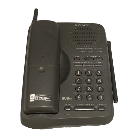
Sony SPP-935 Service Manual
Hide thumbs
Also See for SPP-935:
- Operating instructions manual (62 pages) ,
- Operating instructions manual (62 pages) ,
- Operating instructions manual (60 pages)
Table of Contents
Advertisement
Quick Links
Advertisement
Table of Contents

Related Manuals for Sony SPP-935


Summary of Contents for Sony SPP-935
- Page 1 SPP-935 SERVICE MANUAL US Model SPECIFICATIONS CORDLESS TELEPHONE MICROFILM...
-
Page 2: Table Of Contents
WITH MARK ! ON THE SCHEMATIC DIAGRAMS AND IN THE PARTS LIST ARE CRITICAL TO SAFE OPERATION. TEST MODE REPLACE THESE COMPONENTS WITH SONY PARTS WHOSE 3-1. Base Unit ................. 14 PART NUMBERS APPEAR AS SHOWN IN THIS MANUAL 3-2. Handset ................15 OR IN SUPPLEMENTS PUBLISHED BY SONY. - Page 3 SECTION 1 This section is extracted from instruction manual. GENERAL – 3 –...
- Page 4 – 4 –...
- Page 5 – 5 –...
- Page 6 – 6 –...
- Page 7 – 7 –...
- Page 8 – 8 –...
- Page 9 – 9 –...
- Page 10 – 10 –...
- Page 11 – 11 –...
-
Page 12: Disassembly
SECTION 2 DISASSEMBLY Note: Follow the disassembly procedure in the numerical order given. HAND CABINET (REAR) 2 two screws (BTP3 × 12) 1 Remove the battery case lid to direction of the arrow A . 3 two claws 5 Remove the hand cabinet (rear) to direction of the arrow B . - Page 13 HAND MAIN BOARD 2 two screws (BTP3 × 10) 3 washer 5 Remove the HAND MAIN board to direction of the arrow C . 1 two screws (P2 × 5) 4 antenna (ANT2) 1 two screws (P2 × 5) BASE CABINET (UPPER) 3 base cabinet (upper) 2 claw 1 two screws...
-
Page 14: Test Mode
SECTION 3 TEST MODE [INTERCOM] 3-1. BASE UNIT • Toggle mic mute signal ON/OFF (U12 !™ pin). [Start-up] • CHARGE LED is ON at mic mute enable, off at mic mute disable. 1. When powered up, press and hold keys at the same time for 1 ~ 2 seconds. -
Page 15: Handset
3-2. HANDSET [Start-up] 1. When powered up, press and hold at the same time for 1 ~ 2 seconds. 2. Then press at the same time. 3. Release and press again at the same time to enter testmode, and happy tone is emitted. Default setting: •... -
Page 16: Electrical Adjustments
SECTION 4 ELECTRICAL ADJUSTMENTS 4-1. BASE UNIT SECTION 3. RX LOOP VOLTAGE check Setting: digital voltmeter • Make the set in Test Mode (See page 14) 1. TX LOOP VOLTAGE check TP (RX-LOOP-VOLTAGE) – Setting: digital voltmeter Precedure: • Connect a voltmeter to TP3 (RX-LOOP-VOLTAGE) and GND. TP4 (TX-LOOP-VOLTAGE) •... -
Page 17: Handset Section
4-2. HANDSET SECTION 3. RX LOOP VOLTAGE check Setting: frequency counter • Make the set in test mode (See page 15) 1. TX LOOP VOLTAGE check J2 (RX-LOOP-VOLTAGE) – Setting J2 (GND) digital voltmeter Precedure: J2 (TX-LOOP-VOLTAGE) • Connect a frequency counter to J2 (RX-LOOP-VOLTAGE) and –... -
Page 18: Diagrams
SPP-935 SECTION 5 DIAGRAMS 5-1. BLOCK DIAGRAM – BASE UNIT Section – • SIGNAL PATH : TX (TELEPHONE) : TX (INTERCOM) : RX (TELEPHONE) : RX (INTERCOM) EXPANDER, NIOSE GATE IF AMP, LIMITER AMP, MIX U6 (1/2) : BELL ANT1... -
Page 19: Block Diagram - Handset Section
SPP-935 5-2. BLOCK DIAGRAM – HANDSET Section – EXPANDER, NIOSE GATE IF AMP, LIMITER AMP, MIX U7 (1/2) ANT2 FILTER LIMITER IF AMP DMOD RF AMP IF AMP BUFFER RF AMP IF AMP PRE/SUM B.P.F. U5 (1/3) FILTER FIL2 FIL2... -
Page 20: Note For Printed Wiring Boards And Schematic Diagrams
5-3. NOTE FOR PRINTED WIRING BOARDS AND SCHEMATIC DIAGRAMS • Waveforms – BASE UNIT Section – – HANDSET Section – Note on Schematic Diagram: Note on Printed Wiring Boards: • All capacitors are in µF unless otherwise noted. pF: µµF •... -
Page 21: Printed Wiring Board - Base Main Board (Side A)
SPP-935 5-4. PRINTED WIRING BOARD – BASE MAIN Board (SIDE A) – • Semiconductor Location (SIDE A) Ref. No. Location I-11 G-11 H-12 G-11 F-13 I-12 F-13 G-12 H-12 C-13 D-13 D-13 F-12 F-13 I-12 H-11 H-12 I-11 D-10 J-11... -
Page 22: Printed Wiring Board - Base Main Board (Side B)
SPP-935 5-5. PRINTED WIRING BOARD – BASE MAIN Board (SIDE B) – • Semiconductor Location (SIDE B) Ref. No. Location F-13 G-13 G-13 F-13 G-13 G-12 F-10 E-14 F-10 (Page 33) – 27 – – 28 –... - Page 23 SPP-935 5-6. SCHEMATIC DIAGRAM – BASE MAIN Section (1/2) – • See page 24 for Waveforms. • See page 40 to 42 for IC Block Diagrams. (Page 31) The components identified by mark ! or dotted line with mark ! are critical for safety.
- Page 24 SPP-935 5-7. SCHEMATIC DIAGRAM – BASE MAIN Section (2/2) – • See page 24 for Waveforms. • See page 40 to 42 for IC Block Diagrams. (Page 34) (Page 30) (Page 34) The components identified by mark ! or dotted line with mark ! are critical for safety.
-
Page 25: Printed Wiring Board - Base Key Section
SPP-935 5-8. PRINTED WIRING BOARD – BASE KEY Section – 5-9. SCHEMATIC DIAGRAM – BASE KEY Section – (Page 32) (Page 31) • Semiconductor Location Ref. No. Location (Page 27) Note: • : carbon pattern. – 33 – – 34 –... - Page 26 SPP-935 5-10. SCHEMATIC DIAGRAM – HAND MAIN Section – • See page 24 for Waveforms. • See page 40 to 42 for IC Block Diagrams. – 35 – – 36 –...
-
Page 27: Printed Wiring Board - Hand Main Section
SPP-935 5-11. PRINTED WIRING BOARD – HAND MAIN Section – (Page 40) – 37 – – 38 –... -
Page 28: Printed Wiring Board - Sheet Switch Section
SPP-935 • Semiconductor Location • IC Block Diagrams Ref. No. Location Ref. No. Location U1 MC13156FB (HAND MAIN BOARD) U1 MC13156DWR2 (BASE MAIN BOARD) 23 22 20 19 VEE1 D-13 LO EMIT C-13 DEMOD B-10 LO IN QUAD COIL VCC N/C... - Page 29 U6 TA31103F (BASE MAIN BOARD) U14 MC34119DR2 (BASE MAIN BOARD) U15, 16 MC74HC595AF (BASE MAIN BOARD) U7 TA31103F (HAND MAIN BOARD) 15 14 13 – ∆G – – SWITCH BIAS MUTE CONTROL PRE AMP CIRCUIT VREF VREF – SHIFT REGISTER VREF THROUG VREF...
-
Page 30: Ic Pin Function Description
5-13. IC PIN FUNCTION DESCRIPTION • BASE MAIN BOARD U3 LSC433399FB (SYSTEM CONTROLLER) Pin No. Pin Name Function DTMF EN DTMF tone control signal output to the KS58015D (U17) “H”: enable, “L”: disable EEPROM CS Chip select signal output to the EEPROM (U4) “H” active, Normally: “L” Serial data latch pulse output to the MC74HC595AF (U15) When LATCH 1 goes from “L”... - Page 31 • HAND MAIN BOARD U3 LSC433400FB (SYSTEM CONTROLLER) Pin No. Pin Name Function RX ENABLE RX system power supply on/off control signal output “L”: power on LO BAT Battery level detect signal input from the LP2953IM (U11) “L”: battery low level OPEN Not used (open) 4 to 7...
-
Page 32: Exploded Views
SECTION 6 EXPLODED VIEWS NOTE: • -XX and -X mean standardized parts, so they • Items marked “*” are not stocked since they • The mechanical parts with no reference num- may have some difference from the original are seldom required for routine service. Some ber in the exploded views are not supplied. - Page 33 (2) BASE UNIT SECTION not supplied not supplied ANT1 (including r A) Ref. No. Part No. Description Remark Ref. No. Part No. Description Remark * 51 1-670-653-11 BASE KEY BOARD * 62 A-3672-439-A BASE MAIN BOARD, COMPLETE 1-771-451-11 SWITCH, RUBBER KEY (BASE) 3-026-666-01 CABINET (LOWER), BASE 3-026-669-01 LENS (3 LED) 3-383-270-01 FOOT, RUBBER...
-
Page 34: Electrical Parts List
BASE KEY SECTION 7 ELECTRICAL PARTS LIST BASE MAIN NOTE: • Due to standardization, replacements in the • Items marked “*” are not stocked since they The components identified by mark ! or dotted line with mark parts list may be different from the parts speci- are seldom required for routine service. - Page 35 BASE MAIN Ref. No. Part No. Description Remark Ref. No. Part No. Description Remark 1-162-910-11 CERAMIC CHIP 0.25PF 50V 1-162-909-11 CERAMIC CHIP 0.25PF 50V C135 1-164-004-11 CERAMIC CHIP 0.1uF 1-162-910-11 CERAMIC CHIP 0.25PF 50V C136 1-164-227-11 CERAMIC CHIP 0.022uF C137 1-126-967-11 ELECT 47uF 1-162-919-11 CERAMIC CHIP...
- Page 36 BASE MAIN Ref. No. Part No. Description Remark Ref. No. Part No. Description Remark C194 1-162-968-11 CERAMIC CHIP 0.0047uF 10% 8-729-016-85 TRANSISTOR 2SC4226(R24) T-941-615-31 TRANSISTOR MMBT3904LT1 < DIODE > T-941-615-31 TRANSISTOR MMBT3904LT1 8-719-026-45 DIODE BB535E7989GEG 8-729-041-22 FET CF739R 8-719-026-45 DIODE BB535E7989GEG 8-729-923-31 TRANSISTOR 2SC4083-P 8-719-026-45 DIODE BB535E7989GEG 8-729-923-31 TRANSISTOR 2SC4083-P...
- Page 37 BASE MAIN Ref. No. Part No. Description Remark Ref. No. Part No. Description Remark 1-216-853-11 METAL CHIP 470K 1/16W 1-216-841-11 METAL CHIP 1/16W 1-216-815-11 METAL CHIP 1/16W 1-216-809-11 METAL CHIP 1/16W 1-216-815-11 METAL CHIP 1/16W 1-216-679-11 METAL CHIP 0.5% 1/10W R100 1-216-815-11 METAL CHIP 1/16W...
- Page 38 BASE MAIN HAND MAIN Ref. No. Part No. Description Remark Ref. No. Part No. Description Remark R163 1-216-833-11 METAL CHIP 1/16W < IC > R164 1-216-833-11 METAL CHIP 1/16W R165 1-216-833-11 METAL CHIP 1/16W 8-759-459-06 IC MC13156DWR2 R166 1-218-292-11 RES, CHIP 1/16W 8-759-294-10 IC TB31202FN R167...
- Page 39 HAND MAIN Ref. No. Part No. Description Remark Ref. No. Part No. Description Remark 1-162-908-11 CERAMIC CHIP 0.25PF 50V 1-162-909-11 CERAMIC CHIP 0.25PF 50V 1-162-923-11 CERAMIC CHIP 47PF 1-162-912-11 CERAMIC CHIP 0.5PF 1-162-909-11 CERAMIC CHIP 0.25PF 50V 1-162-923-11 CERAMIC CHIP 47PF 1-162-910-11 CERAMIC CHIP 0.25PF 50V...
- Page 40 HAND MAIN Ref. No. Part No. Description Remark Ref. No. Part No. Description Remark 1-218-653-11 METAL CHIP 0.5% 1/16W 8-719-047-37 DIODE BAS16 1-218-653-11 METAL CHIP 0.5% 1/16W 8-719-047-37 DIODE BAS16 1-216-815-11 METAL CHIP 1/16W 8-719-909-90 DIODE BAV99 8-719-063-75 LED SML-010JT-T86 (INTERCOM) 1-216-817-11 METAL CHIP 1/16W 1-801-729-11 DIODE VARISTOR, CHIP...
- Page 41 HAND MAIN Ref. No. Part No. Description Remark Ref. No. Part No. Description Remark R142 1-216-817-11 METAL CHIP 1/16W 1-216-853-11 METAL CHIP 470K 1/16W R143 1-216-845-11 METAL CHIP 100K 1/16W 1-218-759-11 METAL CHIP 200K 0.5% 1/10W R144 1-216-853-11 METAL CHIP 470K 1/16W 1-216-699-11 METAL CHIP...
- Page 42 Ref. No. Part No. Description Remark Ref. No. Part No. Description Remark ACCESSORIES & PACKING MATERIALS ******************************** 1-475-852-11 ADAPTOR, AC (AC-T122) 1-528-769-11 BATTERY PACK (BP-T23) 1-696-453-21 CORD (WITH MODULAR PLUG) (LINE) (22cm) 1-696-454-11 CORD (WITH MODULAR PLUG) (LINE) (2m15cm) 3-010-356-11 LABEL (MEMORY) 3-012-609-01 SPACER (WALL HOOK) 3-016-278-11 CASE, WALL HOOK 3-862-850-11 MANUAL, INSTRUCTION (ENGLISH, SPANISH)
- Page 43 SPP-935 Sony Corporation 98D0513-1 9-925-927-11 Personal & Mobile Communication Company Printed in Japan © 1998. 4 – 56 – Published by Quality Assurance Dept.
Need help?
Do you have a question about the SPP-935 and is the answer not in the manual?
Questions and answers