Table of Contents
Advertisement
Quick Links
These models are RoHS-compliant. Provide
servicing referring to "NOTES FOR SERVICING
RoHS-COMPLIANT PRODUCTS" described in
the service manual.
CAUTION
Before servicing this chassis, it is important that the service person read the "SAFETY PRECAUTIONS" and "PRODUCT
SAFETY NOTICE" in this service manual.
Copyright C 2006 Mitsubishi Electric Corporation All Rights Reserved.
Pb Solder, Pb Joints, Pb PCA
This product uses lead-free solder
on the circuit boards. For repairing
circuit boards, see "Precautions for
resoldering" in this Service Manual.
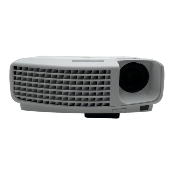
MITSUBISHI ELECTRIC
DLP
TM
PROJECTOR
MODEL
SD420U/SD430U/
XD420U/XD430U/
XD435U/XD435U-G
2006
Advertisement
Table of Contents

Related Manuals for Mitsubishi Electric SD420U


Summary of Contents for Mitsubishi Electric SD420U
- Page 1 Service Manual. CAUTION Before servicing this chassis, it is important that the service person read the “SAFETY PRECAUTIONS” and “PRODUCT SAFETY NOTICE” in this service manual. MITSUBISHI ELECTRIC Copyright C 2006 Mitsubishi Electric Corporation All Rights Reserved.
-
Page 2: Notes For Servicing Rohs-Compliant Products
NOTES FOR SERVICING RoHS-COMPLIANT PRODUCTS Follow the notes and instructions below when servicing RoHS-compliant products. 1. For RoHS-compliant products, be sure to use RoHS-compliant service parts. Check the presence of <G> marking on the rating plate to distinguish RoHS- compliant product from non-RoHS-compliant product. <G>... -
Page 3: Specifications
• Resolution • Audio Input : 350 mV(rms), 10 kΩ or more : RGB : 0.7 V(p-p), 75 Ω(negative sync.) [SD420U / SD430U] • Analog RGB Input : 1,024 × 768 = 786,432 pixels / YC Y : 1.0 V(p-p) , 75 Ω(negative sync.) [XD420U / XD430U / XD435U / XD435U-G] : 0.7 V(p-p), 75 Ω... -
Page 4: Table Of Contents
CONTENTS – FILE “COVERPGE” – – FILE “ELCTADJ” – ELECTCAL ADJUSTMENT ··········································· NOTES FOR SERVICING RoHS-COMPLIANT PRODUCTS ······ Necessary equipment and connecting ····················· SPECIFICATIONS ························································· Test signal ································································ CONTENTS ································································ Adjustment with Microsoft ® Windows ® 98/Me/XP – FILE “EXPOSED” – operating system ················································... -
Page 5: Video Signal
DIAGNOSIS FLOW CHART Video signal : Computer no signal. Video no signal. Abnormal Abnormal Check Check Turn on source. Turn on source. source. source. Normal Normal Abnormal Abnormal Check Check Replace cable. Replace cable. cable. cable. Normal Normal Computer Video Abnormal Abnormal Chang to... - Page 6 Fail to light up. Check Abnormal Look up service manual and follow indication. check point. Normal Check Abnormal Replace lamp lamp power unit and power unit or re- connector. inseert connector. Normal Check PCB- Abnormal Replace PCB- POWER and POWER or re- connector.
- Page 7 No volume. Color missing on screen. Abnormal Abnormal Replace cable or Check Check Replace cable. connect the top cover. cable. cable back. Normal Normal Check Check Abnormal Abnormal Speaker speaker inner Re-connect wire. connector connect. become loose. wire. Normal Normal Abnormal Abnormal Check...
- Page 8 Opereation function : Remote control doesn't work. Button doesn't work. Abnormal Abnormal Check Replace cable or Check Replace battery. connect the battery top cover cable. cable back. level. Normal Normal Abnormal Abnormal Check Check Replace remote Replace button. remote control. button.
- Page 9 Power source : No power source Fan failure after turning on. after turning on. Check Check Abnormal Abnormal Replace Fan connector Lamp lamp cover or become loose. Cover. reassembly. connector. Normal Normal Unplug the power cord, check that LED goes out, Check Abnormal Replace...
- Page 10 DIAGNOSIS INFORMATION Outline of self-diagnosis function This projector is provided with the self-diagnosis function. In case of any failure, the LED at the top of the projector will indicate the failure. Diagnosis result indication LED indication and failures are described in the following table. LED can be reset “automatically” or “by turning on/off of the main power”...
- Page 11 Preferen LED Indication Check Point -tial Symptom Failure Reset POWER STATUS Reference order Replace the lamp and reset the lamp operating Power-on is prohibited because of No power-on time. (Press and hold the Power, , and Manual the end of the lamp life. buttons on the projector together for 3 seconds.) High temperature of the intake air Temperature around the air inlet (on the...
-
Page 12: Operating Conditions
OBTAINING WARNING HISTORY Outline 8. The failure code corresponding to the button you pressed is displayed. Display the warning history of the projector using the - History 1 : The latest failure is displayed. program. Before displaying the warning history, install DLP - History 2 : The second latest failure is displayed. -
Page 13: Specification Of Rgb Signals In Each Computer Mode Of The Projector
The projector’s maximum resolution is 1024 x 768 pixels (800 x supplied to the COMPONENT terminal, the signal mode is indi- 600 pixels for SD420U/SD430U). It may not display images of cated as 480i or 576i. higher reso lutions than 1024 x 768 (or 800 x 600) correctly. -
Page 14: Electrical Adjustments
Monitor for personal COMPUTER IN computer Test signal terminal USB cable • SVGA signal (Vertical frequency 60 Hz) (for SD420U / SD430U) Signal • XGA signal (Vertical frequency 60 Hz) Personal generator Projector computer (for XD420U / XD430U / XD435U / XD435U-G) •... - Page 15 Adjustment with Microsoft ® Windows ® 98/Me/XP operating system 1. Starting 1. Start Windows 98/Me/XP. 2. Select [Start] - [Programs] - [Accessories] - [Communications] - [Hyper Terminal] in order to display the Hyper Terminal window. 2. Hyper terminal setting Item Setting 1.
- Page 16 Model Signal 4. Supply an test signal (White/black, No. 29). 5. Enter [00 ~ 5] (the command for RGB input clamp adjustment) on the Hyper SD420U SVGA Terminal window, and the adjustment proceeds automatically. SD430U 6. When the adjustment finishes, the return command [00 ~ 5111] is displayed on XD420U/XD430U the Hyper Terminal window.
- Page 17 BRIGHTNESS ... . .0 Pattern COLOR TEMP ..STANDARD Built-in red pattern 2. Project an image on the screen. SD420U 3. Display the FUNCTION menu and select [C/W Delay]. The built-in red pattern SVGA_WRGB_64scale signal will be displayed. SD430U...
- Page 18 DMD BIAS VOLTAGE ADJUSTMENT Procedure: Check the bias voltage setting code printed on the DMD chip to be mounted on the DMD PCB ASSY. Change the setting of the DIP switch on the DMD PCB ASSY according to the last letter (B to E) of the code.
-
Page 19: Trademark, Registered Trademark
TRADEMARK, REGISTERED TRADEMARK (Digital Light Processing) and DMD (Digital Micromirror Device) are trademarks of Texas Instruments Incorporated. Other brand or product names are trademarks or registered trademarks of their respective holders. PRODUCT SAFETY NOTICE Many electrical and mechanical parts in the projector have special safety related characteristics. These characteristics are often not evident from visual inspection nor can the protection afforded by them necessarily be obtained by using replacement components rated for higher voltage, etc. -
Page 20: Safety Precautions
SAFETY PRECAUTIONS North america NOTICE: Observe all cautions and safety related notes located inside the cabinet and on the chassis. Warning 1. Operation of this projector outside the cabinet or with the cover removed presents a shock hazard from the projector power supplies. -
Page 21: Precautions For Resoldering
PRECAUTIONS FOR RESOLDERING Lead-free solder is handled in a different way from eutectic solder. See below for details. How to distinguish circuit boards using lead-free solder from those using eutectic solder Circuit boards using lead-free solder A mark of Pb Solder, Pb Joints, Pb PCA or LFS (for limited marking space) is printed near the board assembly number on the component side. -
Page 22: Exposed View Dlp Assy
EXPOSED VIEW DLP ASSY Fig. 1-1 Parts list : See page 2 of PARTS LIST. Part name q TOP COVER w MAIN PCB ASSY e POWER PCB ASSY 4 LENS COVER t BOTTOM COVER 6 LAMP COVER 7 AC SWITCH Table 1-1 - 4 -... -
Page 23: Sub Assy
Sub ASSY Fig. 1-2 Parts list : See page 3 of PARTS LIST. Part name Part name q LAMP POWER UNIT o COOLING FAN (EXHAUST) w THERMISTOR1 !0 COOLING FAN (POWER) e KEYPAD PCB ASSY !1 BACK COVER 4 KEY BUTTON !2 DC OUT PCB ASSY t SPEAKER !3 AC INLET UNIT... -
Page 24: Optical Unit
Optical unit Fig. 1-3 Parts list : See page 3 of PARTS LIST. Part name Part name q THERMISTOR2 6 DMD THERMAL PAD w LIGHT TUNNEL 7 DMD PCB ASSY e CW UNIT i DMD CHIP 4 CW PCB ASSY o LENS UNIT t COOLING FAN (OPTICAL) !0 LAMP... -
Page 25: Disassembly
DISASSEMBLY 1. Removal of the top cover and front ASSY 1. Place the projector upside down as shown in Fig. 2-1-1. 2. Remove the five screws (a) as shown in Fig. 2-1-1. 3. Place the projector bottom down as shown in Fig. 2-1-2. 4. -
Page 26: Removal Of The Main Pcb Assy
2.Removal of the MAIN PCB ASSY 1. Remove the top cover and front ASSY following “1. Removal of the top cover and front ASSY.” 2. Remove the eight screws (a) and one screw (b) as shown in Fig. 2-2-1. 3. Remove the four screws (a) as shown in Fig. 2-2-2. 4. -
Page 27: Removal Of The Lamp Power Unit
3. Removal of the lamp power unit Ballast ASSY 1. Remove the top cover and front ASSY following “1. Removal of the top cover and front ASSY.” 2. Remove the MAIN PCB ASSY following “2. Removal of the MAIN PCB ASSY.” 3. -
Page 28: Removal Of The Optical Unit
4. Removal of the optical unit Back ASSY 1. Remove the top cover and front ASSY following “1. Removal of the top cover and front ASSY.” 2. Remove the MAIN PCB ASSY following “2. Removal of the MAIN PCB ASSY.” 3. -
Page 29: Removal Of The Power Pcb Assy
5. Removal of the POWER PCB ASSY 1. Remove the top cover and front ASSY following “1. Removal of the top cover and front ASSY.” 2. Remove the MAIN PCB ASSY following “2. Removal of the MAIN PCB ASSY.” 3. Remove the ballast ASSY following “3. Removal of the lamp power unit.”... -
Page 30: Removal Of The Ir (F) Pcb Assy,Coolingfan (Exhaust) And Cooling Fan (Power)
7. Removal of the IR(F) PCB ASSY,cooling fan (exhaust) and cooling fan (power) 1. Remove the top cover and front ASSY following “1. Removal of the top cover and front ASSY.” Cooling fan 2. Remove the two screws (a) as shown in Fig. 2-7-1. (power) 3. -
Page 31: Removal Of The Dmd Pcb Assy
10. Removal of the DMD PCB ASSY and DMD chip 1. Remove the top cover and front ASSY following “1. Removal of the top cover and front ASSY.” 2. Remove the MAIN PCB ASSY following “2. Removal of DMD PCB ASSY the MAIN PCB ASSY.”... -
Page 32: Removal Of The Lamp
11. Removal of the lamp 1. Remove the top cover and front ASSY following “1. Removal of the top cover and front ASSY.” 2. Remove the MAIN PCB ASSY following “2. Removal of the MAIN PCB ASSY.” Lamp ASSY 3. Remove the ballast ASSY following “3. Removal of the lamp power unit.”... -
Page 33: Removal Of The Cw Unit
12. Removal of the CW unit and CW PCB ASSY 1. Remove the top cover and front ASSY following “1. Removal of the top cover and front ASSY.” 2. Remove the MAIN PCB ASSY following “2. Removal of the MAIN PCB ASSY.” 3. -
Page 34: Removal Of The Light Tunnel
13. Removal of the light tunnel 1. Remove the top cover and front ASSY following “1. Removal of the top cover and front ASSY.” 2. Remove the MAIN PCB ASSY following “2. Removal of the MAIN PCB ASSY.” 3. Remove the ballast ASSY following “3. Removal of the lamp power unit.”... - Page 35 LIGHT TUNNEL ADJUSTMENT 1. Replace the light tunnel and assemble the optical unit in the reverse order of removal of the light tunnel. Note that the two screws for light tunnel adjustment (a) should be temporarily fastened and should not be sealed by screw lock. Screws for light tunnel adjustment (temporarily fastened without screw lock) 2.
- Page 36 4. Turn the adjustment screws so that the inside of the light tunnel can be viewed completely as shown in the figure and conceptual drawing below. Inadequate adjustment (Inside is partly hidden.) Adequate adjustment (Inside can be viewed completely.) Conceptual drawing Moves in the arrow's direction Inner wall of the...
-
Page 37: Label Position
LABEL POSITION TR label S label C label Name label 0 0 0 1 0 0 1 Lamp label U lens label... -
Page 38: Packing
PACKING werty Parts list : See page 4 of PARTS LIST. Item No. Part name EPE bag Instraction CD Safety manual Remote control VGA cable Composite video cable AC power cord (EU) AC power cord (US) Packing cushion Packing case - 20 -... -
Page 39: Replacing The Lamp
REPLACING THE LAMP When the lamp no longer functions, replace it with a new one. Tighten up the screw (a) using a Phillips screwdriver (+) to secure the lamp Caution: cover. Do not remove the lamp immediately after using the projector. You Reset of the lamp operation time may get burned because the lamp very hot after use. -
Page 40: Maintenance
MAINTENANCE Caution: Be sure to turn off the lamp and unplug the power cor d from the wall outlet before you perform any maintenance on the projector. Cleaning of the projector and the ventilation slots Use a soft cloth to clean the pr ojector and the ventilation grilles. When the grilles become dirty , wipe them with a soft cloth dampened with diluted mild deter gent, and then wipe them with a dry cloth. -
Page 41: Service Commands
SERVICE COMMANDS Display the operation status screen S/W VERSION 1.00 XD430 SET TIME (total) 519H 04M Hold down the [ ], [ ], and [ENTER] buttons on the projector together to LAMP TIME (total) 519H 04M display the picture shown on the right. LAMP TIME (LOW) 519H 04M LAMP RESET... -
Page 42: Replacement Of The Main Pcb Assy
REPLACEMENT OF THE MAIN PCB ASSY Outline When replacing the MAIN PCB ASSY, transfer the factory adjustment data from the old MAIN PCB ASSY to the new MAIN PCB ASSY to write the DDC data into the new MAIN PCB ASSY. There are three ways to transfer the data as follows: (1) Replace the EEPROM (U25). -
Page 43: Function Menu (Setting Menu Only For Service)
FUNCTION MENU ( SETTING MENU ONLY FOR SERVICE ) Displaying the FUNCTION menu 1. Select “LANGUAGE” in the FEATURE menu. 2. Press the “AUTO POSITION,” “ENTER,” and “AUTO POSITION” buttons on the remote control in order. The FUNCTION menu will be displayed. Exiting the FUNCTION menu Press the “MENU”... -
Page 44: Installation Of Dlp Composer (Tm) Lite And Preparations
INSTALLATION OF DLP COMPOSER (TM) LITE AND PREPARATIONS Outline DLP Composer (TM) Lite is a program used for downloading the firmware to the ROM in the projector, adjusting ADC offset, and obtaining the warning history. Select [ALL]. Operating conditions Microsoft ®... - Page 45 When [Hit any key to continue] is displayed on the screen, e Set [Vendor] and [Product]. press any key on the keyboard and wait for the installation process to complete. Product name Vendor Product SD420U/SD430U Preparation XD420U/XD430U 0x784 0x5001 1. Start DLP Composer (TM) Lite. (The dialog shown XD435U/XD435U-G below appears.)
-
Page 46: Download Of The Firmware
[SD420_Flash_v***.img], - [BP_DDP2000_Library_35] : folder [SD430_Flash_v***.img], w Put a checkmark to [Skip [XD420_Flash_v***.img], - [SD420_Flash_v***.img] : Firmware data (for SD420U) Boot Loader Area]. [XD430_Flash_v***.img], or - [SD430_Flash_v***.img] : Firmware data (for SD430U) [XD435_Flash_v***.img] - [XD420_Flash_v***.img] : Firmware data (for XD420U) - [XD430_Flash_v***.img] : Firmware data (for XD430U) -
Page 47: Parts List
PARTS LIST MODEL : SD420U / SD430U / XD420U / XD430U / XD435U / XD435U-G Purpose of this parts list : To expedite delivery of replacement parts ordered. Please specify : 1. Model number/serial number 2. Part number and its description 3. -
Page 48: Exposed View
The parts on this page correspond to those on page 4 in the EXPOSED file. ITEM PART NO. PART NAME DESCRIPTION EXPOSED VIEW DLP ASSY (Fig. 1-1) 750D033O30 TOP COVER [SD420U] 750D033O10 TOP COVER [SD430U] 750D033O20 TOP COVER [XD420U] 750D032O10 TOP COVER... -
Page 49: Sub Assy
CW PCB ASSY 288P298O10 COOLING FAN (OPTICAL) 499D106O30 DMD THERMAL PAD 935D875O60 DMD PCB ASSY 276P209O10 DMD CHIP [SD420U / SD430U] 276P255O10 DMD CHIP [XD420U / XD430U / XD435U / XD435U-G] 490D036O10 LENS UNIT ! 10 253P196O20 LAMP [SD420U / SD420U]... -
Page 50: Packing
ITEM PART NO. PART NAME DESCRIPTION PACKING 772D040O10 EPE BAG 871D495O10 INSTRUCTION CD [SD420U / XD420U] 871D492O10 INSTRUCTION CD [SD430U / XD430U] 871D495O20 INSTRUCTION CD [XD435U / XD435U-G] 871D495O30 SAFETY MANUAL [SD420U / XD420U] 871D492O20 SAFETY MANUAL [SD430U / XD430U]... -
Page 51: Electrical Parts And Others
871D492O10 INSTRUCTION CD [SD430U/XD430U] 276P255O10 DMD CHIP 1076-6002/6008 871D495O20 INSTRUCTION CD [XD435U/XD435U-G] [XD420U/XD430U/XD435U/XD435U-G] 871D495O30 SERVICE MANUAL (SAFETY MANUAL) [SD420U/XD420U] 288P298O10 FAN MOTOR (COOLING FAN(OPTICAL)) 288P299O10 FAN MOTOR (COOLING FAN(EXHAUST)) 871D492O20 SERVICE MANUAL (SAFETY MANUAL) [SD430U/XD430U] 288P300O10 FAN MOTOR (COOLING FAN(POWER)) - Page 52 RoHS SYMBOL PART SYMBOL PART PART NAME TYPE/MODEL PART NAME TYPE/MODEL OTHER CRITICAL COMPONENTS - - - - - - - - - - EMI FILTER WIHT INLET 06SS2-LMG-W - - - - - - - - - - THERMOSTAT YS11-A-140-B-C6 - - - - - - - - - - TRIGGER COIL KP-113...
-
Page 53: Block Diagram
UNIT Color For XD435U/ POWER PCB-CW LAMP BLOCK DIAGRAM XD435U-G Wheel STBY12 L-BOX STBY3.3,DGND PCB-POWER STBYR5 CWINDEX SENSOR Photo-Intrrupter GP2S27C MA18..MA0 (3pin SH) (5pinZ-H) (2pinZ-H) (10pinS-H) (4pinFPC) IS42S16400A STBY3.3-FMT CWCTR, STBY5 CWY1,CWY2,CWY3 STBY1.5-FMT LM393 EXT_ARSTZ PMD1000 MCLK MCLK <<PUMARSTZ>> RIN1- USB-R LD7..LD0 SCLK1... - Page 54 CONNECTOR INFOMATION PCB-MAIN TEMP3 J5 : INTER LOCK SWITCH Pin No. Description J6 : FRONT IR Pin No. Description DGND RSI0 STBY5T J7 : FAN3 (COOLING FAN (LAMP)) Pin No. Description L-FANV L-FGND L-FSTOP J8 : FAN2 (COOLING FAN (EXHAUST)) Pin No.
- Page 55 J9 : FAN1 (COOLING FAN (POWER)) Pin No. Description P-FANV P-FGND P-FSTOP J10 : CW Pin No. Description CWCTR CWY1 CWY2 CWY3 J12 : DC INPUT Pin No. Description AGND STBYR5 POWER2 POW-TEMP FAN-TEMP AGND STBY12 AGND STBY12 AGND J13 : BALLAST CONTROL Pin No.
- Page 56 TEMP4 : THERMISTOR Pin No. Description TMPIN DGND CN2 : KEYPAD CONTROL Pin No. Description LOUT+ LOUT- KEY_0 KEY_1 KEY_2 LEDPWR LEDLMPG LEDLMPR CN3 : CW SENSOR Pin No. Description STBY3.3 CWINDEX DGND...
- Page 57 Con3 Con1 Con2 Con4 J2 : USB Pin No. Description VCCUSB USB_N USB_P AGND AGND AGND J3 : AUDIO OUTPUT Pin No. Description AGND LOUT+ ROUT+ LIN1- RIN1- AGND SE/BTL J4 : AUDIO INPUT Pin No. Description AGND PCI-L PCI-R...
- Page 58 CON1 : RS232 Pin No. Description R2IN T2OUT AGND AGND AGND CON2-1 : COMPUTER INPUT 1 Pin No. Description PCIR PCIG AGND AGND AGND AGND AGND AGND STBY5T AGND AGND AGND VCLK CON2-2 : COMPUTER INPUT 2 Pin No. Description PC2R PC2G PC2B...
- Page 59 CON3 : D-SUB OUTPUT Pin No. Description MRED MGRN MBLU AGND AGND AGND AGND AGND CON4 : S-VIDEO AND VIDEO Pin No. Description AGND AGND AGND COMPIN AGND CN1(Not available in current main board version) Pin No. Description USB5V GNDD AGND AGND AGND...
- Page 60 PCB-POWER Summarize Connector Description AC input 390V output DC output PJ1 : AC INPUT Pin No. Description Line Neutral PJ2 : +380 output AC INPUT Pin No. Description +380 -380...
- Page 61 PJ3 : DC output Pin No. Description AUGND STBY 12AU AGND STBY 12V AGND STBY12V AGND FAN ON Power Temp Power 2 STBY R5 AGND...
- Page 62 LAMP POWER UNIT Control board is installed vertically on the ballast Control board Ballast CN1: Input Pin No. Description DC 370V CN2 : Control signal Pin No. Description Lighting detection signal (collector) Lighting detection signal (emitter) Lighting order signal (common anode) Lighting order signal (cathode) Power change signal (cathode) CN3 : Output...
- Page 65 STBY5 STBY5 TPIN1 TPIN1 STBY3.3 STBY3.3 AGND 56uH 56uH 350mA TPIN2 TPIN2 L7760 L7760 C323 C323 C324 C324 10Kx4 10Kx4 STBY12 STBY12 C326 C326 R4A8 R4A8 STBY12 C322 C322 10uF/16V 10uF/16V 10uF/16V 10uF/16V 100uF/6.3V 100uF/6.3V PRTFANSTOP PRTFANSTOP TPIN3 TPIN3 SMD24PT SMD24PT C1210 C1210...
- Page 68 DEC_SW1.5D DEC_SW3.3D DEC_SW1.5D DEC_SW3.3D C126 C126 C144 C144 C145 C145 C146 C146 C113 C113 C143 C143 0.1uF 0.1uF 0.1uF 0.1uF 0.1uF 0.1uF 0.1uF 0.1uF 0.1uF 0.1uF 0.1uF 0.1uF 0.1uF 0.1uF 0.1uF 0.1uF 0.1uF 0.1uF 0.1uF 0.1uF P2_FLD P2_FLD P2_VSYNC P2H1 P2H1 P2K1 P2K1...
- Page 69 STBY3.3-FMT STBY3.3-FMT R352 R352 R360 R360 0/NC 0/NC STBY5 STBY5 PSA1 PSA1 2SA1576-S/NC 2SA1576-S/NC TXDL TXDL R372NC R372NC TO DDP2000 LSENSE R106100 R106100 PSA2 PSA2 C184 C184 SN74LVC1G07DBVR SN74LVC1G07DBVR DGND 0.1uF 0.1uF RXDL C4220.1uF C4220.1uF RXDL PSA3 PSA3 L35600 L35600 R351 R351 STBY_5...
- Page 70 L58600 L58600 STBY5 L109600 L109600 STBY5 RSII R256 R256 RSII C283 C283 R257 R257 PSM1 PSM1 0.1uF 0.1uF C478 C478 NJM2407R NJM2407R R428 R428 2SA1576AT106R 2SA1576AT106R PSM2 PSM2 SSOP8-065M_KIC SSOP8-065M_KIC 0.1uF 0.1uF RSIO PSM3 PSM3 DAP202KT146 DAP202KT146 STBY5 PDTC124EU PDTC124EU PDTC124EU PDTC124EU R427...
- Page 71 CTMN CTMN STBY3.3-FMT STBY3.3-FMT RD_DQB[0..8] RD_DQB[0..8] 220uF/6.3V 220uF/6.3V S-C63MM S-C63MM RD_RQ[0..7] RD_RQ[0..7] RD_DQA[0..8] RD_DQA[0..8] RD_DQA8 RD_DQA7 0.1uF 0.1uF RD_DQA3 RD_DQA4 DRCGPDZ RD_DQA6 RD_DQA5 DRCGPDZ 0.1uF 0.1uF RD_DQA0 0.1uF 0.1uF RD_DQA1 RD_DQA2 0.1uF 0.1uF 0.1uF 0.1uF CTMN CFMN CFMN 0.1uF 0.1uF 0.1uF 0.1uF K4R271669F-TCS8...
- Page 72 STBY5 STBY5 10uH 10uH C196 C196 STBY5 STBY5 10uH 10uH C421 C421 47uF/6.3V 47uF/6.3V C185 C185 S-C63MM S-C63MM C4200.1uF C4200.1uF 0.1uF 0.1uF 47uF/6.3V 47uF/6.3V R160 R160 2SC3123 2SC3123 C398 C398 S-C63MM S-C63MM R394 R394 R155 R155 2SC3326-B 2SC3326-B C432 C432 R384 R384 SN74LV14APWR...
- Page 73 R261 R261 VCCUSB VCCUSB C289 C289 1000P 1000P USB_N USB_N USB_P USB_P STBY12U KS-001-BNW KS-001-BNW AGND 2.2K 2.2K R255 R255 PC1-L S2B-ZR-SM3A-TF(D)(LF) S2B-ZR-SM3A-TF(D)(LF) 2.2K 2.2K R254 R254 PC1-R R271 R271 R272 R272 C291 C291 C290 C290 SI-3090KM-TL SI-3090KM-TL 470P 470P 470P 470P EPJ-035-33A...
- Page 74 1PS226 1PS226 1PS226 1PS226 1PS226 1PS226 STBY5T2 STBY5T STBYR5T2 STBY5T L106600 L106600 STBYR5T STBYR5T L40600 L40600 2SC3123 2SC3123 C217 C217 CON2-1 CON2-1 C447 C447 C445 C445 C443 C443 C442 C442 C456 C456 47uF/6.3V 47uF/6.3V GSYS R176 R176 R174 R174 S-C63MM S-C63MM GSYS IN0A...
- Page 77 STBY3.3-FMT 5VREF 5VREF STBY3.3-FMT C232 C232 C215 C215 USB_P USB_N USB_P USB_N 0.1uF 0.1uF 0.1uF 0.1uF SN74LVC1G07DBVR SN74LVC1G07DBVR 02237-C05 02237-C05 R170 R170 1.3K 1.3K NC7SB3157P6X NC7SB3157P6X PWM-VOL I2CEN I2CEN R1682.7K R1682.7K SNAD500H/NC SNAD500H/NC LOUT+ LOUT+ IDA1 LOUT- IDA1 LOUT- C2330.1uF C2330.1uF STBY3.3-FMT C2060.1uF...
- Page 84 0x8,1/16W,5% 0x8,1/16W,5% PR37 PR37 0x8,1/16W,5% 0x8,1/16W,5% PR36 PR36 P1_RV[0..7] P1_GY[0..7] P1_BU[0..7] P1_RV[0..7] P1_GY[0..7] P1_BU[0..7] P1_RV0 P1_ARV0 P1_GY0 P1_AGY0 P1_BU0 P1_ABU0 P1_RV1 P1_ARV1 P1_GY1 P1_AGY1 P1_BU1 P1_ABU1 P1_RV2 P1_ARV2 P1_GY7 P1_AGY7 P1_BU2 P1_ABU2 P1_AGY[0..7] P1_RV3 P1_ARV3 P1_GY6 P1_AGY6 P1_BU3 P1_ABU3 P1_AGY[0..7] P1_RV4 P1_ARV4 P1_GY5...
Need help?
Do you have a question about the SD420U and is the answer not in the manual?
Questions and answers