Table of Contents

Subscribe to Our Youtube Channel
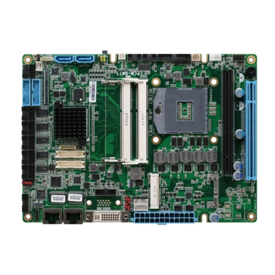
Related Manuals for Aaeon PCM-QM77


Summary of Contents for Aaeon PCM-QM77
- Page 1 PCM-QM77 Compact Board User‟s Manual 3 Last Updated: March 16, 2016...
-
Page 2: Copyright Notice
AAEON assumes no liabilities resulting from errors or omissions in this document, or from the use of the information contained herein. AAEON reserves the right to make changes in the product design without notice to its users. - Page 3 Acknowledgement All other products‟ name or trademarks are properties of their respective owners. Microsoft Windows is a registered trademark of Microsoft Corp. Intel, Pentium, Celeron, and Xeon are registered trademarks of Intel Corporation Core, Atom are trademarks of Intel Corporation ...
- Page 4 Packing List Before setting up your product, please make sure the following items have been shipped: Item Quantity PCM-QM77 17592QM772 Cooler 1702150155 SATA cable 1709070500 SATA Power cable 9657666600 Jumper Cap Product DVD with User‟s Manual (in pdf) and drivers ...
- Page 5 (if any), its specifications, dimensions, jumper/connector settings/definitions, and driver installation instructions (if any), to facilitate users in setting up their product. Users may refer to the AAEON.com for the latest version of this document. Preface...
- Page 6 Safety Precautions Please read the following safety instructions carefully. It is advised that you keep this manual for future references All cautions and warnings on the device should be noted. Make sure the power source matches the power rating of the device. Position the power cord so that people cannot step on it.
- Page 7 If any of the following situations arises, please the contact our service personnel: Damaged power cord or plug Liquid intrusion to the device iii. Exposure to moisture Device is not working as expected or in a manner as described in this manual The device is dropped or damaged Any obvious signs of damage displayed on the device...
- Page 8 FCC Statement This device complies with Part 15 FCC Rules. Operation is subject to the following two conditions: (1) this device may not cause harmful interference, and (2) this device must accept any interference received including interference that may cause undesired operation.
- Page 9 China RoHS Requirements (CN) 产品中有毒有害物质或元素名称及含量 AAEON Main Board/ Daughter Board/ Backplane 有毒有害物质或元素 部件名称 铅 汞 镉 六价铬 多溴联苯 多溴二苯醚 (Pb) (Hg) (Cd) (Cr(VI)) (PBB) (PBDE) 印刷电路板 ○ ○ ○ ○ ○ ○ 及其电子组件 外部信号 ○ ○ ○ ○ ○ ○...
- Page 10 China RoHS Requirement (EN) Poisonous or Hazardous Substances or Elements in Products AAEON Main Board/ Daughter Board/ Backplane Poisonous or Hazardous Substances or Elements Hexavalent Polybrominated Polybrominated Component Lead Mercury Cadmium Chromium Biphenyls Diphenyl Ethers (Pb) (Hg) (Cd) (Cr(VI)) (PBB) (PBDE) PCB &...
-
Page 11: Table Of Contents
Table of Contents Chapter 1 - Product Specifications ..................1 Specifications ......................2 Chapter 2 – Hardware Information ..................5 Dimensions ....................... 6 Jumpers and Connectors ..................8 List of Jumpers ....................... 10 2.3.1 LVDS Port 2 Operating VDD Selection (JP1) ........11 2.3.2 LVDS Port 2 Backlight Inverter VCC Selection (JP1)...... - Page 12 2.4.7 ATX Power Connector (CN7) ............. 21 2.4.8 LVDS Port 2 Inverter / Backlight Connector (CN8) ....... 22 2.4.9 LVDS Port 1 Inverter / Backlight Connector (CN9) ....... 22 2.4.10 Audio In/Out/CD-in and MIC Connector (CN10) ......23 2.4.11 D-SUB CRT Connector (CN11) (Optional) ........23 2.4.12 CRT Connector (CN12) ...............
- Page 13 2.4.35 USB 2.0 Ports 5 and 6 (CN36) ............44 2.4.36 USB 2.0 Ports 7 and 8 (CN37) ............44 2.4.37 PS/2 Keyboard/Mouse Combo Port (CN38) ........45 2.4.38 IrDA Connector (CN39) (Optional)........... 45 2.4.39 SATA Port 2 Connector (CN40) ............46 2.4.40 SATA Port 1 Connector (CN41) ............
- Page 14 3.4.8 Advanced: AMT Configuration ............71 3.4.9 Advanced: USB Configuration ............72 3.4.10 Advanced: F81216 Second Super IO Configuration ....74 3.4.11 Advanced: Super IO Configuration ..........75 3.4.11.1 Super IO Configuration: Serial Port X Configuration ..76 3.4.12 Advanced: Parallel Port Configuration ..........78 3.4.13 Advanced: F81866 H/W Monitor .............
- Page 15 DMA Channel Assignments ................118 Appendix C – Mating Connectors ..................119 List of Mating Connectors and Cables ............120 Appendix D – RAID & AHCI Settings................. 123 Setting RAID ......................124 Setting AHCI ......................131 Appendix E – Electrical Specifications for I/O Ports............135 Electrical Specifications for I/O Ports ...............
-
Page 16: Chapter 1 - Product Specifications
Chapter 1 Chapter 1 - Product Specifications... -
Page 17: Specifications
Specifications System Form Factor 5.25” Compact Board (203 mm x 146 mm) ® ® ™ Processor Intel 3rd Generation Intel Core ® i7/i5/i3/Celeron processor System Memory 204-pin DDR3 SODIMM x 2, DDR3/L 1333/1600, up to 16GB ® Chipset Intel QM77/HM76... - Page 18 (AT mode to control by jumper, and BIOS need to be set ACPI disabled) Board Size 8”(L) x5.75” (W) (203mm x 146mm) Gross Weight 0.88 lb (0.4 Kg) Operating Temperature 32°F~140°F (0°C~60°C) Storage Temperature -40°F~176°F (-40°C~80°C) Operation Humidity 0% ~ 90% relative humidity, non-condensing ...
- Page 19 Mouse x 1 *Note on OS For Linux, AAEON suggests the following: - Kernel 2.6.39 version or later: Set default BIOS/SATA operating mode to IDE - Use Ubuntu 12.04 version or later for better display performance Chapter 1 – Product Specifications...
-
Page 20: Chapter 2 - Hardware Information
Chapter 2 Chapter 2 – Hardware Information... -
Page 21: Dimensions
Dimensions Component Side Chapter 2 – Hardware Information... - Page 22 Solder Side Chapter 2 – Hardware Information...
-
Page 23: Jumpers And Connectors
Jumpers and Connectors Component Side Chapter 2 – Hardware Information... - Page 24 Solder Side Chapter 2 – Hardware Information...
-
Page 25: List Of Jumpers
List of Jumpers Please refer to the table below for all of the board‟s jumpers that you can configure for your application Label Function LVDS Port 2 Operating VDD Selection and Backlight Inverter VCC Selection LVDS Port 1 Backlight Lightness Control Mode Selection LVDS Port 2 Backlight Lightness Control Mode Selection LVDS Port 1 Operating VDD Selection and Backlight Inverter VCC Selection... -
Page 26: Lvds Port 2 Operating Vdd Selection (Jp1)
2.3.1 LVDS Port 2 Operating VDD Selection (JP1) +3.3V (Default) 2.3.2 LVDS Port 2 Backlight Inverter VCC Selection (JP1) +12V +5V (default) 2.3.3 LVDS Port 1 Backlight Lightness Control Mode Selection (JP2) 1 2 3 1 2 3 VR mode PWM mode (default) 2.3.4 LVDS Port 2 Backlight Lightness Control Mode Selection (JP3) 1 2 3... -
Page 27: Lvds Port 1 Operating Vdd Selection (Jp4)
2.3.5 LVDS Port 1 Operating VDD Selection (JP4) +3.3V (Default) 2.3.6 LVDS Port 1 Backlight Inverter VCC Selection (JP4) +12V +5V (default) 2.3.7 COM6 Pin9 Function Selection (JP5) Ring (default) +12V 2.3.8 COM2 Pin9 Function Selection (JP6) Ring (default) +12V Chapter 2 –... -
Page 28: At/Atx Power Supply Mode Selection (Jp8)
2.3.9 AT/ATX Power Supply Mode Selection (JP8) 1 2 3 1 2 3 ATX mode (default) AT mode 2.3.10 Front Panel Connector (JP9) Signal PWR_BTN- PWR_BTN+ HDD_LED- HDD_LED+ SPEAKER- SPEAKER+ PWR_LED- PWR_LED+ H/W RESET- H/W RESET+ Chapter 2 – Hardware Information... -
Page 29: Clear Me Jumper (Jp10)
2.3.10 Clear ME Jumper (JP10) Normal (default) Clear ME Note: Clear ME needs to be done after clearing COMS. Two jumpers are needed 2.3.11 Clear CMOS Jumper (JP10) Normal (default) Clear CMOS 2.3.12 Touch Screen 4/5-Wire Mode Selection (JP11) (Optional) 1 2 3 1 2 3 4-wire mode (default) -
Page 30: List Of Connectors
List of Connectors Please refer to the table below for all of the board‟s connectors that you can configure for your application Label Function DVI Connector Stereo Audio Output Connector Ethernet#2 Connector (Optional) Ethernet#1 Connector (Optional) RJ-45 Ethernet#2 Connector RJ-45 Ethernet#1 Connector ATX Power Connector LVDS Port 2 Inverter / Backlight Connector LVDS Port 1 Inverter / Backlight Connector... - Page 31 CN24 COM Port 5 CN25 PCI Slot CN26 COM Port 8 CN27 COM Port 7 CN28 PCI-Express[x16]Slot CN29 DDR3 SO-DIMM Channel B Slot CN30 DDR3 SO-DIMM Channel A Slot CN31 COM Port 10 CN32 COM Port 9 CN34 USB 3.0 Ports 1 and 2 CN35 USB 3.0 Ports 3 and 4 CN36...
-
Page 32: Dvi Connector (Cn1)
2.4.1 DVI Connector (CN1) C3 C4 Pin Name Signal Type Signal Level TMDS_DAT2+ DIFF TMDS_DAT2- DIFF DVI_DDC_CLK DVI_DDC_DATA VSYNC TMDS_DAT1- DIFF TMDS_DAT1+ DIFF TMDS_DAT3- DIFF TMDS_DAT3+ DIFF HPLG_DETECT TMDS_DAT0- DIFF TMDS_DAT0+ DIFF Chapter 2 – Hardware Information... -
Page 33: Stereo Audio Output Connector (Cn2)
TMDS_CLK+ DIFF TMDS_CLK- DIFF GREEN BLUE HSYNC GND_ANALOG 2.4.2 Stereo Audio Output Connector (CN2) PIN4 PIN3 PIN2 PIN1 Pin Name Signal Type Signal Level SPK_OUT_R+ SPK_OUT_R- SPK_OUT_L+ SPK_OUT_L- 2.4.3 Ethernet#2 Connector (CN3) (Optional) MDI0+ MDI0- MDI1+ MDI1- MDI2+ MDI2- MDI3+ MDI3- Pin Name Signal Type... -
Page 34: Ethernet#1 Connector (Cn4) (Optional)
MDI0- DIFF MDI1+ DIFF MDI1- DIFF MDI2+ DIFF MDI2- DIFF MDI3+ DIFF MDI3- DIFF 2.4.4 Ethernet#1 Connector (CN4) (Optional) MDI0+ MDI0- MDI1+ MDI1- MDI2+ MDI2- MDI3+ MDI3- Pin Name Signal Type Signal Level MDI0+ DIFF MDI0- DIFF MDI1+ DIFF MDI1- DIFF MDI2+ DIFF... -
Page 35: Ethernet#2 Connector (Cn5)
2.4.5 RJ-45 Ethernet#2 Connector (CN5) Pin Name Signal Type Signal Level MDI0+ DIFF MDI0- DIFF MDI1+ DIFF MDI2+ DIFF MDI2- DIFF MDI1- DIFF MDI3+ DIFF MDI3- DIFF 2.4.6 RJ-45 Ethernet#1 Connector (CN6) Pin Name Signal Type Signal Level MDI0+ DIFF MDI0- DIFF MDI1+... -
Page 36: Atx Power Connector (Cn7)
2.4.7 ATX Power Connector (CN7) PIN1 PIN12 PIN13 PIN24 Pin Name Signal Type Signal Level +3.3V +3.3V +3.3V +3.3V PWR_OK +5VSB +12V +12V +12V +12V +3.3V +3.3V +3.3V +3.3V -12V -12V PS_ON# Chapter 2 – Hardware Information... -
Page 37: Lvds Port 2 Inverter / Backlight Connector (Cn8)
2.4.8 LVDS Port 2 Inverter / Backlight Connector (CN8) BLK_PWR BKL_CONTROL BKL_ENABLE Pin Name Signal Type Signal Level BKL_PWR +5V / +12V BKL_CONTROL BKL_ENABLE 2.4.9 LVDS Port 1 Inverter / Backlight Connector (CN9) BLK_PWR BKL_CONTROL BKL_ENABLE Pin Name Signal Type Signal Level BKL_PWR +5V / +12V... -
Page 38: Audio In/Out/Cd-In And Mic Connector (Cn10)
LVDS1 BKL_CONTROL can be set by JP2. 2.4.10 Audio In/Out/CD-in and MIC Connector (CN10) MIC_R MIC_L GND_AUDIO CD_GND LINE_L_IN CD_L LINE_R_IN CD_GND CD_R GND_AUDIO RIGHT_OUT LEFT_OUT GND_AUDIO GND_AUDIO Pin Name Signal Type Signal Level MIC_R MIC_L GND_AUDIO CD_GND LINE_L_IN CD_L LINE_R_IN CD_GND GND_AUDIO... -
Page 39: Crt Connector (Cn12)
Pin Name Signal Type Signal Level GREEN BLUE RED_GND_RTN GREEN_GND_RTN BLUE_GND_RTN DDC_DATA HSYNC VSYNC DDC_CLK 2.4.12 CRT Connector (CN12) GREEN BLUE DDC_DATA HSYNC VSYNC CRT_PLUG# DDC_CLK Pin Name Signal Type Signal Level GREEN Chapter 2 – Hardware Information... -
Page 40: Msata Slot (Cn13)
BLUE DDC_DATA HSYNC VSYNC DDC_CLK 2.4.13 mSATA Slot (CN13) Pin Name Signal Type Signal Level +3.3V +3.3V +1.5V +1.5V Chapter 2 – Hardware Information... - Page 41 SATA_TX+ DIFF +3.3V +3.3V SATA_TX- DIFF +1.5V +1.5V SMB_CLK +3.3V SATA_RX- DIFF SMB_DATA +3.3V SATA_RX+ DIFF Chapter 2 – Hardware Information...
-
Page 42: Ethernet#1 Led Indicator (Cn14)
+3.3V +3.3V +3.3V +3.3V +1.5V +1.5V +3.3V +3.3V 2.4.14 Ethernet#1 LED Indicator (CN14) PIN1 PIN2 PIN3 PIN4 PIN5 PIN6 Pin Name Signal Type Signal Level ACT_LED+ ACT_LED- 100_LED+ 100_LED- 1000_LED+ 1000_LED- Chapter 2 – Hardware Information... -
Page 43: Com Port 2 (Cn15)
2.4.15 COM Port 2 (CN15) RI/+5V/+12V RS-232 Pin Name Signal Type Signal Level ± 5V ± 5V ± 5V RI/+5V/+12V IN/ PWR +5V/+12V RS422_TX- RS422_TX+ RS422_RX+ RS422_RX- NC/+5V/+12V RS-422 Pin Name Signal Type Signal Level RS422_TX- ± 5V RS422_TX+ ± 5V RS422_RX+ RS422_RX- Chapter 2 –... - Page 44 NC/+5V/+12V +5V/+12V RS485_D- RS485_D+ NC/+5V/+12V RS-485 Pin Name Signal Type Signal Level RS485_D- ± 5V RS485_D+ ± 5V NC/+5V/+12V +5V/+12V Note: COM2 RS-232/422/485 can be set by BIOS setting. Default is RS-232. COM2 Pin 9 function can be set by JP6. Chapter 2 –...
-
Page 45: Com Port 1 (Cn16)
2.4.16 COM Port 1 (CN16) Pin Name Signal Type Signal Level ± 9V ± 9V ± 9V 2.4.17 Ethernet#2 LED Indicator (CN17) PIN1 PIN2 PIN3 PIN4 PIN5 PIN6 Pin Name Signal Type Signal Level ACT_LED+ ACT_LED- 100_LED+ 100_LED- 1000_LED+ Chapter 2 – Hardware Information... -
Page 46: Lvds Port 2 (Cn18)
1000_LED- 2.4.18 LVDS Port 2 (CN18) PIN 29 PIN 30 PIN 1 PIN 2 Pin Name Signal Type Signal Level BKL_ENABLE BKL_CONTROL LCD_PWR +3.3V/+5V LVDS_A_CLK- DIFF LVDS_A_CLK+ DIFF LCD_PWR +3.3V/+5V LVDS_DA0- DIFF LVDS_DA0+ DIFF LVDS_DA1- DIFF LVDS_DA1+ DIFF LVDS_DA2- DIFF LVDS_DA2+ DIFF LVDS_DA3-... -
Page 47: Com Port 4 (Cn19)
LVDS_DA3+ DIFF DDC_DATA +3.3V DDC_CLK +3.3V LVDS_DB0- DIFF LVDS_DB0+ DIFF LVDS_DB1- DIFF LVDS_DB1+ DIFF LVDS_DB2- DIFF LVDS_DB2+ DIFF LVDS_DB3- DIFF LVDS_DB3+ DIFF LCD_PWR +3.3V/+5V LVDS_B_CLK- DIFF LVDS_B_CLK+ DIFF 2.4.19 COM Port 4 (CN19) Pin Name Signal Type Signal Level ± 9V ±... -
Page 48: Com Port 3 (Cn20)
± 9V 2.4.20 COM Port 3 (CN20) Pin Name Signal Type Signal Level ± 9V ± 9V ± 9V Chapter 2 – Hardware Information... -
Page 49: Lvds Port 1 (Cn21)
2.4.21 LVDS Port 1 (CN21) PIN 29 PIN 30 PIN 1 PIN 2 Pin Name Signal Type Signal Level BKL_ENABLE BKL_CONTROL LCD_PWR +3.3V/+5V LVDS_A_CLK- DIFF LVDS_A_CLK+ DIFF LCD_PWR +3.3V/+5V LVDS_DA0- DIFF LVDS_DA0+ DIFF LVDS_DA1- DIFF LVDS_DA1+ DIFF LVDS_DA2- DIFF LVDS_DA2+ DIFF LVDS_DA3- DIFF... -
Page 50: Lpc Port (Cn22)
DDC_DATA +3.3V DDC_CLK +3.3V LVDS_DB0- DIFF LVDS_DB0+ DIFF LVDS_DB1- DIFF LVDS_DB1+ DIFF LVDS_DB2- DIFF LVDS_DB2+ DIFF LVDS_DB3- DIFF LVDS_DB3+ DIFF LCD_PWR +3.3V/+5V LVDS_B_CLK- DIFF LVDS_B_CLK+ DIFF Note: LVDS1 LCD_PWR can be set to +3.3V or +5V by JP4. 2.4.22 LPC Port (CN22) LAD0 LAD1 LAD2... -
Page 51: Com Port 6 (Cn23)
LAD2 +3.3V LAD3 +3.3V +3.3V +3.3V LFRAME# LRESET# +3.3V LCLK LDRQ0 LDRQ1 SERIRQ +3.3V 2.4.23 COM Port 6 (CN23) RS-232 Pin Name Signal Type Signal Level ± 5V ± 5V ± 5V RI/+5V/+12V IN/ PWR +5V/+12V Chapter 2 – Hardware Information... - Page 52 RS-422 Pin Name Signal Type Signal Level RS422_TX- ± 5V RS422_TX+ ± 5V RS422_RX+ RS422_RX- NC/+5V/+12V +5V/+12V RS485_D- RS485_D+ NC/+5V/+12V RS-485 Pin Name Signal Type Signal Level RS485_D- ± 5V RS485_D+ ± 5V Chapter 2 – Hardware Information...
-
Page 53: Com Port 5 (Cn24)
NC/+5V/+12V +5V/+12V Note: 1. COM6 RS-232/422/485 can be set by BIOS setting. Default is RS-232. 2. COM6 Pin 9 function can be set by JP5. 3. COM6/ IrDA Function can be set by BIOS setting. Default is COM6 Function. 2.4.24 COM Port 5 (CN24) Pin Name Signal Type... -
Page 54: Com Port 8 (Cn26)
2.4.26 COM Port 8 (CN26) Pin Name Signal Type Signal Level ± 9V ± 9V ± 9V 2.4.27 COM Port 7 (CN27) Pin Name Signal Type Signal Level ± 9V ± 9V Chapter 2 – Hardware Information... -
Page 55: Pcie [X16] Slot (Cn28)
± 9V 2.4.28 PCIe [x16] Slot (CN28) Standard specification 2.4.29 DDR3 SO-DIMM Channel B Slot (CN29) Standard specification 2.4.30 DDR3 SO-DIMM Channel A Slot (CN30) Standard specification 2.4.31 COM Port 10 (CN31) Pin Name Signal Type Signal Level ± 9V ±... -
Page 56: Com Port 9 (Cn32)
± 9V 2.4.32 COM Port 9 (CN32) Pin Name Signal Type Signal Level ± 9V ± 9V ± 9V Chapter 2 – Hardware Information... -
Page 57: Usb 3.0 Ports 1 And 2 (Cn34)
2.4.33 USB 3.0 Ports 1 and 2 (CN34) PIN1 PIN19 PIN11 PIN10 Pin Name Signal Type Signal Level +5VSB USB1_SSRX− DIFF USB1_SSRX+ DIFF USB1_SSTX− DIFF USB1_SSTX+ DIFF USB1_D- DIFF USB1_D+ DIFF USB2_D+ DIFF USB2_D- DIFF USB2_SSTX+ DIFF USB2_SSTX− DIFF USB2_SSRX+ DIFF USB2_SSRX−... -
Page 58: Usb 3.0 Ports 3 And 4 (Cn35)
2.4.34 USB 3.0 Ports 3 and 4 (CN35) PIN1 PIN19 PIN11 PIN10 Pin Name Signal Type Signal Level +5VSB USB3_SSRX− DIFF USB3_SSRX+ DIFF USB3_SSTX− DIFF USB3_SSTX+ DIFF USB3_D- DIFF USB3_D+ DIFF USB4_D+ DIFF USB4_D- DIFF USB4_SSTX+ DIFF USB4_SSTX− DIFF USB4_SSRX+ DIFF USB4_SSRX−... -
Page 59: Usb 2.0 Ports 5 And 6 (Cn36)
2.4.35 USB 2.0 Ports 5 and 6 (CN36) +5VSB USB5_D- USB5_D+ USB6_D+ USB6_D- +5VSB Pin Name Signal Type Signal Level +5VSB USB5_D- DIFF USB5_D+ DIFF USB6_D+ DIFF USB6_D- DIFF +5VSB 2.4.36 USB 2.0 Ports 7 and 8 (CN37) +5VSB USB7_D- USB7_D+ USB8_D+ USB8_D-... -
Page 60: Ps/2 Keyboard/Mouse Combo Port (Cn38)
USB7_D+ DIFF USB8_D+ DIFF USB8_D- DIFF +5VSB 2.4.37 PS/2 Keyboard/Mouse Combo Port (CN38) KB_DATA KB_CLK +5VSB MS_CLK MS_DATA Pin Name Signal Type Signal Level KB_ DATA KB_CLK +5VSB MS_DATA MS_CLK 2.4.38 IrDA Connector (CN39) (Optional) IRRX IRTX Chapter 2 – Hardware Information... -
Page 61: Sata Port 2 Connector (Cn40)
Pin Name Signal Type Signal Level IRRX IRTX Note: COM6 / IrDA Function can be set by BIOS setting. Default is COM6 2.4.39 SATA Port 2 Connector (CN40) Pin 1 Pin 7 Pin Name Signal Type Signal Level SATA_TX+ DIFF SATA_TX- DIFF SATA_RX-... -
Page 62: Output For Sata Hdd (Cn43)
Pin Name Signal Type Signal Level SATA_TX+ DIFF SATA_TX- DIFF SATA_RX- DIFF SATA_RX+ DIFF 2.4.41 +5V Output for SATA HDD (CN43) Pin Name Signal Type Signal Level 2.4.42 LPT Connector (CN44) DIO Mode STROBE# AFD# ERROR# DIO0 PRINT# DIO1 SLIN# DIO2 DIO3 ACK#... - Page 63 AFD# ERROR# PRINT# SLIN# ACK# BUSY SLCT Chapter 2 – Hardware Information...
-
Page 64: System Fan Connector (Cn45)
2.4.43 System Fan Connector (CN45) FAN_TAC FAN_POWER Pin Name Signal Type Signal Level FAN_POWER +12V FAN_TAC 2.4.44 Digital IO Port 1 Connector (CN46) DIO0 DIO1 DIO2 DIO3 DIO4 DIO5 DIO6 DIO7 Pin Name Signal Type Signal Level DIO0 DIO1 DIO2 DIO3 DIO4 DIO5... -
Page 65: Digital Io Port 2 Connector (Cn47)
2.4.45 Digital IO Port 2 Connector (CN47) DIO0 DIO1 DIO2 DIO3 DIO4 DIO5 DIO6 DIO7 Pin Name Signal Type Signal Level DIO0 DIO1 DIO2 DIO3 DIO4 DIO5 DIO6 DIO7 2.4.46 Touch Screen Connector (CN48) (Optional) 8 Wires 4 Wires 5 Wires TOP EXCITE UL(Y) BOTTOM EXCITE... - Page 66 BOTTOM LEFT RIGHT 4 Wires 5 Wires UL(Y) BOTTOM UR(H) LEFT LL(L) RIGHT LR(X) SENSE(S) 5-wire Pin Name Signal Type Signal Level UL(Y) UR(H) LL(L) LR(X) SENSE(S) Note: Touch mode can be set by JP11 Chapter 2 – Hardware Information...
-
Page 67: Cpu Fan Connector (Cn49)
2.4.47 CPU FAN Connector (CN49) FAN_TAC FAN_POWER FAN_CTL Pin Name Signal Type Signal Level FAN_POWER +12V FAN_TAC FAN_CTL +3.3V 2.4.48 UIM Card Connector (CN50) Pin Name Signal Type Signal Level UIM_PWR UIM_RST UIM_CLK UIM_VPP UIM_DATA 2.4.49 MiniCard Slot (CN51) Pin Name Signal Type Signal Level PCIE_WAKE#... - Page 68 +1.5V +1.5V PCIE_CLK_REQ# UIM_PWR UIM_DATA PCIE_REF_CLK- DIFF UIM_CLK PCIE_REF_CLK+ DIFF UIM_RST UIM_VPP W_DISABLE# +3.3V PCIE_RST# +3.3V PCIE_RX- DIFF +3.3VSB +3.3V PCIE_RX+ DIFF +1.5V +1.5V Chapter 2 – Hardware Information...
- Page 69 SMB_CLK +3.3V PCIE_TX- DIFF SMB_DATA +3.3V PCIE_TX+ DIFF USB_D- DIFF USB_D+ DIFF +3.3VSB +3.3V +3.3VSB +3.3V +1.5V +1.5V +3.3VSB +3.3V Chapter 2 – Hardware Information...
-
Page 70: Cfast Slot (Cn52)
2.4.50 CFast Slot (CN52) Pin Name Signal Type Signal Level SATA_TX+ DIFF SATA_TX- DIFF SATA_RX- DIFF SATA_RX+ DIFF PC10 PC11 PC12 PC13 +3.3V +3.3V PC14 +3.3V +3.3V PC15 PC16 PC17 Chapter 2 – Hardware Information... -
Page 71: Chapter 3 - Bios Setup
Chapter 3 Chapter 3 - BIOS Setup... -
Page 72: System Test And Initialization
System Test and Initialization The board uses certain routines to perform testing and initialization. If an error, fatal or non-fatal, is encountered, a few short beeps or an error message will be outputted. The board can usually continue the boot up sequence with non-fatal errors. The system configuration verification routines check the current system configuration against the values stored in the CMOS memory. -
Page 73: Ami Bios Setup
AMI BIOS Setup The AMI BIOS ROM has a pre-installed Setup program that allows users to modify basic system configurations, which is stored in the battery-backed CMOS RAM and BIOS NVRAM so that the information is retained when the power is turned off. To enter BIOS Setup, press <Del>... -
Page 74: Setup Submenu: Main
Setup submenu: Main Options summary: (default setting) System Date Day MM:DD:YYYY Change the month, year and century. The „Day‟ is changed automatically. System Time HH : MM : SS Change the clock of the system. Chapter 3 – BIOS Setup... -
Page 75: Setup Submenu: Advanced
Options summary: (default setting) ICC Spread Spectrum Disabled Enabled Spread Spectrum Support AAEON ICC Spread Spectrum AAEON ICC Spread Spectrum default value ACPI Settings System ACPI Parameters S5 RTC Wake Settings Enable system to wake from S5 using RTC alarm. Trusted Computing... - Page 76 Trusted Computing Settings CPU Configuration CPU Configuration Parameters Dynamic Digital IO Configuration DIO setting SATA Configuration SATA Device Options Settings Intel TXT(LT) Configuration Intel Trusted Execution Technology AMT Configuration AMT Configuration Parameters USB Configuration USB Configuration Parameters F81216 Second Super IO Configuration Second IO Configuration Parameters F81866 Super IO Configuration Super IO Configuration Parameters...
-
Page 77: Advanced: Acpi Management
3.4.1 Advanced: ACPI Management Options summary: (default setting) Suspend Disabled S1 only(CPU Stop Clock) ACPI Sleep State S3 only(Suspend to RAM) Both S1 and S3 available for OS to choose from Select the ACPI state used for System Suspend Chapter 3 – BIOS Setup... -
Page 78: Advanced: Rtc Wake Settings
3.4.2 Advanced: RTC Wake Settings Options summary: (default setting) Wake system with Fixed Disabled Time Enabled Enable or disable System wake on alarm event. Wake up time is setting by following settings. Wake up day 0-31 Select 0 for daily system wake up Wake up hour 0-23 Wake up minute... - Page 79 Wake up second 0-59 Wake system with Dynamic Disabled Time Enabled Enable or disable System wake on alarm event. Wake up time is current time + Increase minutes. Wake up minute increase Chapter 3 – BIOS Setup...
-
Page 80: Advanced: Trusted Computing
3.4.3 Advanced: Trusted Computing Options summary: (default setting) Security Device Support Disabled Enabled En/Disable TPM support. TPM State Disabled Enabled En/Disable TPM functionality. Pending TPM Operation None Enable Take Ownership Disable Take Ownership TPM Clear Chapter 3 – BIOS Setup... -
Page 81: Advanced: Cpu Configuration
Select one-time TPM operation. Item value returns to „None‟ after next POST. 3.4.4 Advanced: CPU Configuration Options summary: (default setting) Hyper-Threading Disabled Enabled En/Disable CPU Hyper-Threading function Active Processor Cores 1 to Max CPU cores Number of CPU cores to be active. Intel Virtualization Disabled Technology... -
Page 82: Advanced: Dynamic Digital Io Configuration
En/Disable Intel VT-x function 3.4.5 Advanced: Dynamic Digital IO Configuration Options summary: (default setting) Digital Port X(GPXX) Direction Input Output Set GPIOx as Input or Output Digital Port X(GPXX) Levels Set GPIO output level when used as output pin Chapter 3 – BIOS Setup... -
Page 83: Advanced: Sata Configuration
3.4.6 Advanced: SATA Configuration Options summary: (default setting) SATA Controller(s) Disabled Enabled En/Disable SATA controller Configure SATA as AHCI RAID Configure SATA controller operating as IDE/AHCI/RAID mode. SATA Controller Speed Gen1 Gen2 Gen3 Chapter 3 – BIOS Setup... - Page 84 Indicates the maximum speed the SATA controller can support. Port X Disabled Enabled En/Disable the selected port. Hot Plug Disabled Enabled En/Disable Hot Plug feature for specified port. Chapter 3 – BIOS Setup...
-
Page 85: Advanced: Intel Txt (Lt) Configuration
3.4.7 Advanced: Intel TXT (LT) Configuration Options summary: (default setting) Intel TXT(LT) Support Disabled Enabled En/Disable Intel TXT function. This function only can be enabled/disabled if SMX, VT-x and VT-d support are enabled prior to it. Chapter 3 – BIOS Setup... -
Page 86: Advanced: Amt Configuration
3.4.8 Advanced: AMT Configuration Options summary: (default setting) Intel AMT Enabled Disabled En/Disable Intel® Active Management Technology BIOS Extension. Note: iAMT H/W is always enabled. This option just controls the BIOS extension execution. If enabled, this requires additional firmware in the SPI device Un-Configure ME Enabled Disabled... -
Page 87: Advanced: Usb Configuration
3.4.9 Advanced: USB Configuration Options summary: (default setting) Legacy USB Support Enabled Disabled Auto Enables BIOS Support for Legacy USB Support. When enabled, USB can be functional in legacy environment like DOS. AUTO option disables legacy support if no USB devices are connected. - Page 88 Device Name Auto (Emulation Type) Floppy Forced FDD Hard Disk CD-ROM If Auto. USB devices less than 530MB will be emulated as Floppy and remaining as Floppy and remaining as hard drive. Forced FDD option can be used to force a HDD formatted drive to boot as FDD(Ex.
-
Page 89: Advanced: F81216 Second Super Io Configuration
3.4.10 Advanced: F81216 Second Super IO Configuration Options summary: (default setting) Serial Port 7/8/9/10 Configuration Set Parameters of Serial Port 7/8/9/10 Chapter 3 – BIOS Setup... -
Page 90: Advanced: Super Io Configuration
3.4.11 Advanced: Super IO Configuration Options summary: (default setting) Serial Port 1/2/3/4/5/6 Configuration Set Parameters of Serial Port 1/2/3/4/5/6 Parallel Port Configuration Set Parameters of Parallel Port. ERP MODE Disabled Configure ERP Power Control. Chapter 3 – BIOS Setup... -
Page 91: Super Io Configuration: Serial Port X Configuration
3.4.11.1 Super IO Configuration: Serial Port X Configuration Options summary: (default setting) Serial Port Disabled Enabled En/Disable specified serial port. Change Settings Auto IO=2F8h; IRQ=3; IO=3F8h; IRQ=3,4,5,7,10,11,12; IO=2F8h; IRQ=3,4,5,7,10,11,12; IO=3E8h; IRQ=3,4,5,7,10,11,12; IO=2E8h; IRQ=3,4,5,7,10,11,12; Select a resource setting for Super IO device. Chapter 3 –... - Page 92 Device Type RS232 RS422 RS485 Configure COM2/6 operated as RS232, RS422 or RS485. Chapter 3 – BIOS Setup...
-
Page 93: Advanced: Parallel Port Configuration
3.4.12 Advanced: Parallel Port Configuration Options summary: (default setting) Parallel Port Disabled Enabled En/Disable parallel port. Change Settings Auto IO=378h; IRQ=7; IO=378h; IRQ=5,7,10,11,12; IO=278h; IRQ=5,7,10,11,12; IO=3BCh; IRQ=5,7,10,11,12; Select a resource setting for Super IO device. Device Mode STD Printer Mode Chapter 3 –... - Page 94 SPP Mode EPP-1.9 and SPP Mode EPP-1.7 and SPP Mode ECP Mode ECP and EPP 1.9 Mode ECP and EPP 1.7 Mode Change the Printer Port mode Chapter 3 – BIOS Setup...
-
Page 95: Advanced: F81866 H/W Monitor
3.4.13 Advanced: F81866 H/W Monitor Options summary: (default setting) Smart Fan Function Disabled Enabled Enable or Disable Smart Fan Smart Fan Mode configuration Smart Fan Mode select Chapter 3 – BIOS Setup... -
Page 96: Advanced: Smart Fan Configuration
3.4.14 Advanced: Smart Fan Configuration Options summary: (default setting) Fan 1/2 Smart Fan Control Manual Duty Mode Auto Duty-Cycle Mode Manual Duty Mode: Manually controlling the fan with a given control PWM. Auto Duty-Cycle Mode: Automatically controlling the fan with given parameters. Manual Duty Mode 1 to 100, default is 80/90 Fan Speed value between 1 to 100... - Page 97 Duty Cycle 0/1/2/3/4 1 to 100, default is 100/85/70/60/50 Auto fan speed control. Fan speed will follow different temperature by different duty cycle 1-100 Chapter 3 – BIOS Setup...
-
Page 98: Advanced: Cpu Ppm Configuration
3.4.15 Advanced: CPU PPM Configuration Options summary: (default setting) EIST Disabled Enabled Enable/Disable Intel SpeedStep Turbo Mode Disabled Enabled Turbo Mode enable/disable Chapter 3 – BIOS Setup... -
Page 99: Setup Submenu: Chipset
Setup submenu: Chipset Options summary: (default setting) PCH-IO Configuration South Bridge Parameters System Agent (SA) Configuration SA Parameters Chapter 3 – BIOS Setup... -
Page 100: Chipset: Pch-Io Configuration
3.5.1 Chipset: PCH-IO Configuration Options summary: (default setting) Power Mode ATX Type AT Type Enable or disable „It is now safe to turn off your computer. ‟ string PCI Express Configuration PCI Express Configuration settings PCH Azaliz Configuration PCH Azaliz Configuration settings 82583V LAN Controller Enabled Chapter 3 –... - Page 101 Disabled En/Disabled Intel 82583V NIC PCH LAN Controller Enabled Disabled En/Disabled onboard NIC Wake on LAN Enabled Disabled En/Disabled integrated LAN to wake the system. (The Wake on LAN cannot be disabled if ME is on at Sx state. Restore AC Power Loss Power Off Power On Last State...
-
Page 102: Chipset: System Agent (Sa) Configuration
3.5.2 Chipset: System Agent (SA) Configuration Options summary: (default setting) VT-d Disabled Enabled Check to enable VT-d function on MCH Graphics Configuration Config Graphics Settings Chapter 3 – BIOS Setup... -
Page 103: System Agent (Sa) Configuration: Graphics Configuration
3.5.2.1 System Agent (SA) Configuration: Graphics Configuration Options summary: (default setting) Primary Display Auto IGFX Select graphic adapters to boot Internal Graphics Auto Disabled Enabled En/Disabled internal graphics device DVMT Pre-Allocated 64MB Chapter 3 – BIOS Setup... - Page 104 32MB~1024MB Select DVMT 5.0 Pre-Allocated (Fixed) Graphics Memory size used by the Internal Graphics Device. DVMT Total Gfx Mem 128MB 256MB Select DVMT 5.0 Total Graphic Memory size used by the Internal Graphics Device. Chapter 3 – BIOS Setup...
-
Page 105: Graphics Configuration: Lcd Control
3.5.2.2 Graphics Configuration: LCD Control Options summary: (default setting) Primary IGFX Boot Display VBIOS LVDS LVDS2 CRT+LVDS1 Select Primary IGFX boot display device LVDS1 Control Disabled Enabled Enable or Disable Internal LVDS Chapter 3 – BIOS Setup... - Page 106 LVDS2 Control Disabled Enabled Enable or Disable Onboard CH7511 LVDS1/LVDS2 Panel Type 640x480,18-Bit,60Hz 800x480,18-Bit,60Hz 800x600,18-Bit,60Hz 1024x600,18-Bit,60Hz 1024x768,18-Bit,60Hz 1024x768,24-Bit,60Hz 1280x768,24-Bit,60Hz 1280x1024,48-Bit,60Hz 1366x768,24-Bit,60Hz 1440x900,24Bit,60Hz 1600x1200,48-Bit,60Hz 1920x1080,48-Bit,60Hz 640x480,24-Bit,60Hz 800x600,24-Bit,60Hz 1280x768,18-Bit,60Hz Select panel native resolution. LVDS1/LVDS2 Backlight Inverted Type Normal Select Backlight control type. Inverted: Brightest for low PWM duty cycle and low voltage.
- Page 107 Select Backlight Level Chapter 3 – BIOS Setup...
-
Page 108: Setup Submenu: Boot
Setup submenu: Boot Options summary: (default setting) Quiet Boot Disabled Enabled En/Disable showing boot logo. Launch PXE OpROM policy Disabled Enabled En/Disable PXE boot for LAN Boot Option #X/ XXXX Drive BBS Priorities The order of boot priorities. Chapter 3 – BIOS Setup... -
Page 109: Boot: Bbs Priorities
3.6.1 Boot: BBS Priorities Options summary: (default setting) Boot Option #x Disabled Device name Sets the system boot order Chapter 3 – BIOS Setup... -
Page 110: Setup Submenu: Security
Setup submenu: Security Options summary: (default setting) Administrator Password/ Not set User Password Change User/Administrator Password You can set a User Password once an Administrator Password is set. The password will be required during boot up, or when the user enters the Setup utility. - Page 111 your password (you can enter no more than six letters or numbers). Press Enter to confirm your entry, after which you will be prompted to retype your password for a final confirmation. Press Enter again after you have retyped it correctly.
-
Page 112: Setup Submenu: Save & Exit
Setup submenu: Save & Exit Options summary: (default setting) Save Changes and Exit Exit system setup after saving the changes Discard Changes and Exit Exit system setup without saving any changes Save Changes and Reset Reset the system after saving the changes Discard Changes and Reset Save Changes Save Changes done so far to any of the setup options. -
Page 113: Chapter 4 - Drivers Installation
Chapter 4 Chapter 4 – Drivers Installation... -
Page 114: Product Cd/Dvd
Product CD/DVD The PCM-QM77 comes with a product DVD that contains all the drivers and utilities you need to setup your product. Insert the DVD and follow the steps in the autorun program to install the drivers. In case the program does not start, follow the sequence below to install the drivers. - Page 115 Step 3 – Install LAN Driver Open the STEP3 – LAN folder and select your OS Open the .exe file in the folder Follow the instructions Drivers will be installed automatically Step 4 – Install Audio Driver Open the STEP4 – TXE folder and select your OS Open the .exe file in the folder Follow the instructions Drivers will be installed automatically...
- Page 116 Step 8 – Install Touch Driver Open the STEP8 – Touch folder and select your OS Open the Setup.exe file in the folder Follow the instructions Drivers will be installed automatically Step 9 – Install USB 3.0 Drivers (Windows 7 only) Open the STEP5 - USB3.0 folder followed by Setup.exe Follow the instructions Drivers will be installed automatically...
- Page 117 For Windows 7: Change User Account Control settings to Never notify Chapter 4 – Driver Installation...
- Page 118 Reboot and log in as administrator Chapter 4 – Driver Installation...
- Page 119 Run patch.bat as administrator Chapter 4 – Driver Installation...
-
Page 120: Appendix A - Watchdog Timer Programming
Appendix A Appendix A - Watchdog Timer Programming... -
Page 121: Watchdog Timer Registers
A.1 Watchdog Timer Registers PCM-QM77 Rev.B utilizes Fintek 81666 chipset as its watchdog timer controller. Below are the procedures to complete its configuration and the AAEON intial watchdog timer program is also attached based on which you can develop customized program to fit your application. - Page 122 There are three steps to complete the configuration setup: (1) Enter the MB PnP Mode; (2) Modify the data of configuration registers; (3) Exit the MB PnP Mode. Undesired result may occur if the MB PnP Mode is not exited normally. (1) Enter the MB PnP Mode To enter the MB PnP Mode, four special I/O write operations are to be performed during Wait for Key state.
- Page 123 Watch Dog Timer 1, 2, 3 Control Register (Index=F5h,F6h,FAh Default=00h) Appendix A – Watchdog Timer Programming...
-
Page 124: F81866 Watchdog Timer Initial Program
A.2 F81866 Watchdog Timer Initial Program Main(){ aaeonSuperIOOpen(); aaeonWdtSetCountMode(BOOL bMinute); // Set wdt count mode aaeonWdtSetTimeoutCount(BYTE tTimeout); // Set wdt timer aaeonWdtSetEnable(BOOL bEnable); // Enable wdt aaeonSuperIOClose(); Void aaeonSuperIOOpen(){ // Config F81866 Entry key aaeonioWritePortByte(F81866_INDEX, 0x87); aaeonioWritePortByte(F81866_INDEX, 0x87); Void aaeonWdtSetCountMode(BOOL bMinute){ BYTE WDT_CONTROL = f81866ReadByte(F81866_WDT_CONTROL_REG);... - Page 125 Void aaeonWdtSetEnable(BOOL bEnable){ f81866SetLdn(0x07); if(bEnable){ f81866WriteByte(0x30, 0x01); WDT_BASE_ADDR = (f81866ReadByte(F81866_WDT_BASEADDR_REG_MSB) << 8) | f81866ReadByte(F81866_WDT_BASEADDR_REG_LSB); WDT_STATUS = f81866ReadByte(F81866_WDT_CONTROL_REG); f81866WriteByte(F81866_WDT_CONTROL_REG, WDT_STATUS | 0x20); WDT_STATUS = f81866ReadByte(F81866_WDT_PME_REG); f81866WriteByte(F81866_WDT_PME_REG, WDT_STATUS | 0x01); }else{ f81866WriteByte(0x30, 0x00); WDT_BASE_ADDR = 0; WDT_STATUS = f81866ReadByte(F81866_WDT_CONTROL_REG); f81866WriteByte(F81866_WDT_CONTROL_REG, WDT_STATUS & 0xDF); WDT_STATUS = f81866ReadByte(F81866_WDT_PME_REG);...
-
Page 126: Appendix B - I/O Information
Appendix B Appendix B - I/O Information... -
Page 127: I/O Address Map
I/O Address Map Appendix B – I/O Information... - Page 128 Appendix B – I/O Information...
-
Page 129: Memory Address Map
Memory Address Map Appendix B – I/O Information... -
Page 130: Irq Mapping Chart
IRQ Mapping Chart Appendix B – I/O Information... - Page 131 Appendix B – I/O Information...
- Page 132 Appendix B – I/O Information...
-
Page 133: Dma Channel Assignments
DMA Channel Assignments Appendix B – I/O Information... -
Page 134: Appendix C - Mating Connectors
Appendix C Appendix C – Mating Connectors... -
Page 135: List Of Mating Connectors And Cables
0110-01-553-300 Connector COM Port 4 Serial 17011002 CN19 PINREX 52A-90-10GB00 Connector Port COM Port 3 Serial 17011002 CN20 PINREX 52A-90-10GB00 Connector Port LVDS#1 CN21 E-call 0110-01-553-300 Connector AAEON 17031201 CN22 LPC Port PINREX 710-73-12TW01 Cable Appendix C – Mating Connectors... - Page 136 COM Port 6 Serial 17011002 CN23 PINREX 52A-90-10GB00 Connector Port COM Port 5 Serial 17011002 CN24 PINREX 52A-90-10GB00 Connector Port COM Port 8 Serial 17011002 CN26 PINREX 52A-90-10GB00 Connector Port COM Port 7 Serial 17011002 CN27 PINREX 52A-90-10GB00 Connector Port COM Port Serial 17011002...
- Page 137 Cable System Fan CN45 CATCH 1190-700-03S Connector DIO #1 CN46 PINREX 52A-90-10GB00 Connector DIO #2 CN47 PINREX 52A-90-10GB00 Connector Touch CN48 Screen PINREX 710-73-09TW01 Connector CPU Fan CN49 CATCH 1190-700-042 Connector Appendix C – Mating Connectors...
-
Page 138: Appendix D - Raid & Ahci Settings
Appendix D Appendix D – RAID & AHCI Settings... -
Page 139: Setting Raid
Setting RAID OS installation to SETUP RAID Mode f6fly-x86.zip Step 1: Extract the from “Driver CD -> Step7-RAID&AHCI\WinXP_32” and copy below files to diskette. Step 2: Connect the USB Floppy drive to the board and insert the diskette from previous step. Step 3: Configure SATA Controller to RAID mode in BIOS SETUP Menu: Advanced ->... - Page 140 Step 4: Configure DVD/CD-ROM drive as the first boot device. Step 5: Save changes and exit BIOS SETUP Appendix D – RAID & AHCI Settings...
- Page 141 Step 6: Press CTRL-I to enter RAID Configuration Utility Step 7: Choose “1. Create RAID Volume” Appendix D – RAID & AHCI Settings...
- Page 142 Step 8 – Configure RAID parameters for the system Step 9 – Choose “Create Volume” and confirmed in next warning message. Appendix D – RAID & AHCI Settings...
- Page 143 Step 10 – Exit RAID Configuration Utility and Reboot to DVD/CD-ROM device to install Step 11 – Press “F6” to install RAID driver Appendix D – RAID & AHCI Settings...
- Page 144 Step 12 – Press “S” to install RAID driver Step 13 – Choose “Intel(R) Mobile Express Chipset SATA RAID Controller” Appendix D – RAID & AHCI Settings...
- Page 145 Step 14 – It will show the model you selected and then press ”ENTER”. Windows Setup will continue to install OS. Appendix D – RAID & AHCI Settings...
-
Page 146: Setting Ahci
Setting AHCI OS installation to SETUP AHCI Mode f6fly-x86.zip Step 1: Extract the from “Driver CD -> Step7 - RAID&AHCI\WinXP_32” and copy below files to diskette. Step 2: Connect the USB Floppy drive to the board and insert the diskette from previous step. - Page 147 Step 4: Configure DVD/CD-ROM drive as the first boot device. Step 5: Save changes and exit BIOS SETUP Appendix D – RAID & AHCI Settings...
- Page 148 Step 6 – Boot to DVD/CD-ROM device to install OS Step 7 – Press “F6” to install AHCI driver Step 8 – Press “S” to install AHCI driver Appendix D – RAID & AHCI Settings...
- Page 149 Step 9 – Choose “Intel(R) 7 Series Chipset Family SATA AHCI Controller” Step 10 – It will show the model you selected and then press ”ENTER”. Windows Setup will continue to install OS. Appendix D – RAID & AHCI Settings...
-
Page 150: Appendix E - Electrical Specifications For I/O Ports
Appendix E Appendix E – Electrical Specifications for I/O Ports... -
Page 151: Electrical Specifications For I/O Ports
Electrical Specifications for I/O Ports Reference Signal Name Rate Output DVI Ports +5V/0.5A LVDS Port 2 Inverter +5V/2A or / Backlight BKL_PWR +12V/2A Connector LVDS Port 1 Inverter +5V/2A or / Backlight BKL_PWR +12V/2A Connector VGA Ports CN11/CN12 +5V/1A (reserved) mSATA CN13 +3.3V... - Page 152 Combo Port IrDA Connector CN39 +5V/0.5A +5V Output for CN43 +5V/1A SATA HDD System FAN CN45 FAN_POWER +12V/0.5A DIO0~DIO7 +5V/(Open drain) Digital IO Port1 CN46 +5V/1A DIO0~DIO7 +5V/(Open drain) Digital IO Port2 CN47 +5V/1A CPU FAN CN49 FAN_POWER +12V/0.5A +3.3VSB +3.3V/1.1A Mini-Card Slot CN51...
-
Page 153: Appendix F - Digital I/O Ports
Appendix F Appendix F – Digital I/O Ports... -
Page 154: Digital I/O Ports
Digital I/O Ports The F75111 provides one serial access interface, I2C Bus, to read/write internal registers. The address of Serial Bus is 0x6E (0110_1110) The related register for configuring DIO is list as follows: Configuration and Control Register-Index 01h Power-on default [7:0]=0000_1000b Name Description Software reset for all registers... - Page 155 GPIO2x Output Control Register-Index 20h Power-on default [7:0]=0000_0000b Name Description GPIO 27 output control. Set to 1 for GP27_OCTRL VSB3V output function. Set to 0 for input function (default). GPIO 26 output control. Set to 1 for GP26_OCTRL output function. Set to 0 for input VSB3V function (default).
- Page 156 GP22_ODATA VSB3V GPIO 22 output data. GP21_ODATA VSB3V GPIO 21 output data. GP20_ODATA VSB3V GPIO 20 output data. GPIO2x Input Status Register-Index 22h Power-on default [7:0]=xxxx_xxxxb Name Description GP27_PSTS VSB3V Read the GPIO27 data on the pin. GP26_PSTS VSB3V Read the GPIO26 data on the pin. GP25_PSTS VSB3V Read the GPIO25 data on the pin.
- Page 157 mov cl,20h call CT_I2CWriteByte mov cl,22h call CT_I2CReadByte ;Input : CL - register index CH - device ID ;Output : AL - Value read Ct_I2CReadByte Proc Near mov ch,06eh dx, 0f040h + 00h ; Host Control Register al, 0ffh ; Clear previous commands dx, al call Delay5ms...
- Page 158 al, al ; Clear old data dx, al dx, 0f040h + 02h ; Host Control Reegister al, 48h ; Start a byte access dx, al call CT_Chk_SMBus_Ready dx, 0f040h + 05h al, dx Ct_I2CReadByte Endp ;Input : CL - register index CH - device ID AL - Value to write ;Output: none...
- Page 159 dx, 0f040h + 04h ; Transmit Slave Address Register mov al, ch ; Set the slave address and dx, al ; prepare for a WRITE command dx, 0f040h + 03h ; Host Command Register al, cl ; offset to write dx, al mov dx, 0f040h + 05h mov al, ah...
- Page 160 al,dx ;get status call Delay5ms dx,al ;clear status call Delay5ms test al, 02H ;termination of command ? short Clear_final al, NOT 40H ;mask INUSE bit al,al ;status OK ? short Clear_final test al,04h ;device error short SMBus_Err loop short Chk_I2c_OK ;SMbus error due to timeout SMBus_Err: Clear_final:...
- Page 161 Appendix F – Digital I/O Ports...
Need help?
Do you have a question about the PCM-QM77 and is the answer not in the manual?
Questions and answers