Table of Contents
Advertisement
Quick Links
Advertisement
Table of Contents

Related Manuals for Telit Wireless Solutions GC864-QUAD V2


Summary of Contents for Telit Wireless Solutions GC864-QUAD V2
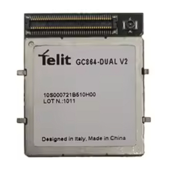
- Page 1 GC864 QUAD V2 GC864 DUAL V2 Hardware User Guide 1vv0300874 Rev.1 – 2010-03-29...
-
Page 2: Applicability Table
GC864 Hardware User Guide 1vv0300874 Rev.1 – 2010-03-29 APPLICABILITY TABLE PRODUCT GC864-QUAD V2 GC864-DUAL V2 GC864-QUAD V2 with SH Reproduction forbidden without Telit Communications S.p.A. written authorization - All Rights Reserved. Page 2 of 64... - Page 3 GC864 Hardware User Guide 1vv0300874 Rev.1 – 2010-03-29 DISCLAIMER The information contained in this document is the proprietary information of Telit Communications S.p.A. and its affiliates (“TELIT”). The contents are confidential and any disclosure to persons other than the officers, employees, agents or subcontractors of the owner or licensee of this document, without the prior written consent of Telit, is strictly prohibited.
-
Page 4: Table Of Contents
GC864-QUAD V2 / GC864-DUAL V2 M ..............12 ODULE ONNECTIONS 3.3. PIN-OUT................................13 3.3.1. GC864-QUAD V2 / GC864-DUAL V2 Antenna Connector ..............16 HARDWARE COMMANDS........................ 17 4.1. GC864-QUAD V2 / GC864-DUAL V2 ................... 17 URNING 4.2. GC864-QUAD V2 / GC864-DUAL V2 ................. 19 URNING 4.2.1. - Page 5 Description ............................56 10.13.2. Using ADC Converter ........................57 ASSEMBLY THE GC864-QUAD V2 / GC864-DUAL V2 ON THE BOARD .......... 58 11.1.1. Debug of the GC864-QUAD V2 / GC864-DUAL V2 in Production ............. 59 PACKING SYSTEM ........................60 CONFORMITY ASSESSMENT ISSUES ..................61 SAFETY RECOMMENDATIONS ....................
-
Page 6: Introduction
1.1. Scope The aim of this document is the description of some hardware solutions useful for developing a product with the Telit GC864-QUAD V2 / GC864-DUAL V2 module. 1.2. Audience This document is intended for Telit customers, who are integrators, about to implement their applications using our GC864-QUAD V2 / GC864-DUAL V2 module. -
Page 7: Document Organization
Chapter 2: “Overview” provides an overview of the document. Chapter 3: “GC864-QUAD V2 / GC864-DUAL V2 Mechanical Dimensions” Chapter 4: “GC864-QUAD V2 / GC864-DUAL V2 Module Connections” deals with the pin out configuration and layout. Chapter 5: “Hardware Commands” How to control the module via hardware. -
Page 8: Text Conventions
GC864 Hardware User Guide 1vv0300874 Rev.1 – 2010-03-29 1.5. Text Conventions Danger – This information MUST be followed or catastrophic equipment failure or bodily injury may occur. Caution or Warning Alerts the user to important points about integrating the – module, if these points are not followed, the module and end user equipment may fail or malfunction. -
Page 9: Document History
GC864 Hardware User Guide 1vv0300874 Rev.1 – 2010-03-29 1.7. Document History ISSUE#0 2010-01-25 Release First ISSUE# 0 ISSUE#1 2010-03-29 Updated Par.4.1, Par.5.1, Par.6.1 Reproduction forbidden without Telit Communications S.p.A. written authorization - All Rights Reserved. Page 9 of 64... -
Page 10: Overview
Telit GC864-QUAD V2 / GC864-DUAL V2 module. For further hardware details that may not be explained in this document refer to the Telit GC864-QUAD V2 / GC864-DUAL V2 Product Description document where all the hardware information is reported. -
Page 11: Gc864 Mechanical Dimensions
GC864 Hardware User Guide 1vv0300874 Rev.1 – 2010-03-29 GC864 Mechanical Dimensions The Telit GC864-QUAD V2 / GC864-DUAL V2 module overall dimensions are: • Length: 36.2 mm • Width: 30 mm • Thickness: 3.2 mm • Weight: 4.8g Reproduction forbidden without Telit Communications S.p.A. written authorization - All Rights Reserved. -
Page 12: Mechanical View Of Telit Gc864-Quad V2 With Sim Holder
GC864 Hardware User Guide 1vv0300874 Rev.1 – 2010-03-29 3.1. Mechanical View of Telit GC864-QUAD V2 with SIM Holder 3.2. GC864-QUAD V2 / GC864-DUAL V2 Module Connections Reproduction forbidden without Telit Communications S.p.A. written authorization - All Rights Reserved. Page 12 of 64... -
Page 13: Pin-Out
GC864 Hardware User Guide 1vv0300874 Rev.1 – 2010-03-29 3.3. PIN-OUT The GC864-QUAD V2 / GC864-DUAL V2 uses a 80 pin Molex p.n. 53949-0878 male connector for the connections with the external applications. This connector matches the 54150-0878 models. Internal Signal... - Page 14 CMOS 2.8V Input command for switching power ON or OFF (toggle command). The Ω ON/OFF* pulse to be sent to the GC864-QUAD V2 / GC864-DUAL V2 must be Pull up to VBATT equal or greater than 1 second. RESET* Reset input...
- Page 15 Reserved Reserved Reserved Reserved NOTE: The GC864-QUAD V2 / GC864-DUAL V2 Modules has one DVI ports on the system interface. NOTE: Reserved pins must not be connected. NOTE: RTS must be connected to the GND (on the module side) if flow control is not used.
-
Page 16: Gc864-Quad V2 / Gc864-Dual V2 Antenna Connector
SERVICE connection 3.3.1. GC864-QUAD V2 / GC864-DUAL V2 Antenna Connector The GC864-QUAD V2 / GC864-DUAL V2 module is equipped with a 50 Ω RF connector from Murata, GSC type P/N MM9329-2700B. The counterpart suitable is Murata MXTK92 Type or MXTK88 Type. -
Page 17: Hardware Commands
4.1. Turning ON the GC864-QUAD V2 / GC864-DUAL V2 To turn the GC864-QUAD V2 / GC864-DUAL V2 on, the pad ON# must be tied low for at least 1000ms and then released. A pulse duration less than 1000ms should also start the power on procedure, but this is not guaranteed. - Page 18 GC864 Hardware User Guide 1vv0300874 Rev.1 – 2010-03-29 For example: 1- Let us assume you need to drive the ON# pad with a totem pole output of a +3/5 V microcontroller (uP_OUT1): 2- Let us assume you need to drive the ON# pad directly with an ON/OFF button: A flow chart with proper turn on procedure is detailed below: Reproduction forbidden without Telit Communications S.p.A.
-
Page 19: Turning Off The Gc864-Quad V2 / Gc864-Dual V2
4.2. Turning OFF the GC864-QUAD V2 / GC864-DUAL V2 Turning off of the device can be done in three ways: • by software command (see GC864-QUAD V2 / GC864-DUAL V2 Software User Guide) • by tying low pin ON# Either ways, the device issues a detach request to network informing that the device will not be reachable any more. -
Page 20: Hardware Unconditional Restart
Do not use any pull up resistor on the RESET* line nor any totem pole digital output. Using pull up resistor may cause latch up problems on the GC864-QUAD V2 / GC864- DUAL V2 power regulator and improper functioning of the module. The line RESET* must be connected only in open collector configuration. - Page 21 GC864 Hardware User Guide 1vv0300874 Rev.1 – 2010-03-29 In the following flow chart is detailed the proper restart procedure: For example: 1- Let us assume you need to drive the RESET# pad with a totem pole output of a +3/5 V microcontroller (uP_OUT2): Reproduction forbidden without Telit Communications S.p.A.
-
Page 22: Power Supply
Nominal Supply Voltage 3.80 V Normal operating Voltage Range 3.40 V - 4.20 V Extended operating Voltage Range 3.22 V – 4.50 V The GC864-QUAD V2 / GC864-DUAL V2 power consumptions are: GC864-QUAD V2 / GC864-DUAL V2 Average Mode Mode description (mA) -
Page 23: General Design Rules
GC864 Hardware User Guide 1vv0300874 Rev.1 – 2010-03-29 The GSM system is made in a way that the RF transmission is not continuous but it is packed into bursts at a base frequency of about 216 Hz. The relative current peaks can be as high as about 2A. - Page 24 • A Bypass low ESR capacitor of adequate capacity must be provided in order to cut the current absorption peaks close to the GC864-QUAD V2 / GC864-DUAL V2, a 100μF tantalum capacitor is usually suited. •...
- Page 25 A switching power supply will be preferable because of its better efficiency especially with the 2A peak current load represented by the GC864-QUAD V2 / GC864-DUAL V2. • When using a switching regulator, a 500kHz (or more) switching frequency regulator is preferable, because of its smaller inductor size and its faster transient response.
- Page 26 GC864 Hardware User Guide 1vv0300874 Rev.1 – 2010-03-29 An example of switching regulator with 12V input is in the schematic below (split in 2 parts): Reproduction forbidden without Telit Communications S.p.A. written authorization - All Rights Reserved. Page 26 of 64...
-
Page 27: 5.2.2. Thermal Design Guidelines
DO NOT USE any Ni-Cd, Ni-MH, and Pb battery types directly connected with GC864- QUAD V2 / GC864-DUAL V2. Their use can lead to overvoltage on the GC864-QUAD V2 / GC864-DUAL V2 and damage it. USE ONLY Li-Ion battery types. -
Page 28: Power Supply Pcb Layout Guidelines
As far as the heat generated by the GC864-QUAD V2 / GC864-DUAL V2, you can consider it to be during transmissions of 1W max during CSD/VOICE calls and 2W max during class10 GPRS upload. -
Page 29: Parameters For Atex Applications
5.2.4. Parameters for ATEX Applications In order to integrate the Telit GC864-QUAD V2 / GC864-DUAL V2 module into an ATEX application, the appropriate reference standard IEC EN xx and integrations shall be followed. Below are listed parameters and useful information to integrate the module in your application: •... - Page 30 GC864 Hardware User Guide 1vv0300874 Rev.1 – 2010-03-29 • In abnormal conditions, the maximum RF output power may be up to 34 dBm. For this particular application, we recommend the customer to involve TTSC (Telit Technical Support Center) in the design phase of the application. Reproduction forbidden without Telit Communications S.p.A.
-
Page 31: Antenna
6.1. GSM Antenna Requirements As suggested on the Product Description the antenna for a Telit GC864-QUAD V2 / GC864-DUAL V2 device shall fulfill the following requirements: ANTENNA REQUIREMENTS Frequency range... -
Page 32: Gsm Antenna - Installation Guidelines
GC864 Hardware User Guide 1vv0300874 Rev.1 – 2010-03-29 6.2. GSM Antenna – Installation Guidelines • Install the antenna in a place covered by the GSM signal. • The Antenna must be installed to provide a separation distance of at least 20 cm from all persons and must not be co-located or operating in conjunction with any other antenna or transmitter;... -
Page 33: Logic Level Specifications
Where not specifically stated, all the interface circuits work at 2.8V CMOS logic levels. The following table shows the logic level specifications used in the Telit GC864-QUAD V2 / GC864-DUAL V2 interface circuits: Absolute Maximum Ratings – Not Functional Parameter Input level on any -0.3V... -
Page 34: Reset Signal
GC864-QUAD V2 / GC864-DUAL V2 is reset. When the device is reset it stops any operation. After the release of the reset GC864-QUAD V2 / GC864-DUAL V2 is unconditionally shut down, without doing any detach operation from the network where it is registered. -
Page 35: Serial Ports
The only configuration that does not need a level translation is the 2.8V UART. The serial port on the GC864-QUAD V2 / GC864-DUAL V2 is a +2.8V UART with all the 7 RS232 signals. It differs from the PC-RS232 in the signal polarity (RS232 is reversed) and levels. - Page 36 GC864-QUAD V2 / GC864-DUAL V2 side these signal are on the opposite direction: TXD on the application side will be connected to the receive line (here named TXD/ rx_uart ) of the GC864-QUAD V2 / GC864-DUAL V2 serial port and vice versa for RX.
-
Page 37: Rs232 Level Translation
8.2. RS232 Level Translation In order to interface the Telit GC864-QUAD V2 / GC864-DUAL V2 with a PC com port or a RS232 (EIA/TIA-232) application a level translator is required. This level translator must •... - Page 38 1vv0300874 Rev.1 – 2010-03-29 NOTE: In order to be able to do in circuit reprogramming of the GC864-QUAD V2 / GC864- DUAL V2 firmware, the serial port on the Telit GC864-QUAD V2 / GC864-DUAL V2 shall be available for translation into RS232 and either it is controlling device shall be placed into tristate, disconnected or as a gateway for the serial data when module reprogramming occurs.
-
Page 39: Uart Level Translation
GC864 Hardware User Guide 1vv0300874 Rev.1 – 2010-03-29 The RS232 serial port lines are usually connected to a DB9 connector with the following layout: 8.3. 5V UART Level Translation If the OEM application uses a microcontroller with a serial port (UART) that works at a voltage different from 2.8 –... - Page 40 NOTE: The UART input line TXD (rx_uart) of the GC864-QUAD V2 / GC864-DUAL V2 is NOT internally pulled up with a resistor, so there may be the need to place an external 47KΩ pull-up resistor, either the DTR (dtr_uart) and RTS (rts_uart) input lines are not pulled up internally, so an external pull-up resistor of 47KΩ...
-
Page 41: Audio Section Overview
For these reasons we have not changed the acronyms, keeping them in the Software and on the schematics. The Base Band Chip of the GC864-QUAD V2 / GC864-DUAL V2Telit Modules maintains the same architecture. For more information and suggestions refer to Telit document: •... - Page 42 Mic HF+ MIC P2 100nF Microphone Balanced Mic HF- MIC N2 100nF Single ended xgaffull.skd GC864-QUAD V2 / GC864-DUAL V2 Audio Front End Block Diagram Reproduction forbidden without Telit Communications S.p.A. written authorization - All Rights Reserved. Page 42 of 64...
-
Page 43: Electrical Characteristics
GC864 Hardware User Guide 1vv0300874 Rev.1 – 2010-03-29 9.2. Electrical Characteristics TIP: Being the microphone circuitry the more noise sensitive, its design and layout must be done with particular care. Both microphone paths are balanced and the OEM circuitry must be balanced designed to reduce the common mode noise typically generated on the ground plane. -
Page 44: Output Lines Characteristics
GC864 Hardware User Guide 1vv0300874 Rev.1 – 2010-03-29 9.2.2. Output Lines Characteristics TIP: We suggest driving the load differentially from both output drivers, thus the output swing will double and the need for the output coupling capacitor avoided. However if Single Ended circuitry particular OEM application needs also a can be implemented,... - Page 45 GC864 Hardware User Guide 1vv0300874 Rev.1 – 2010-03-29 “EAR_MT” Output Lines line coupling AC single-ended DC differential 0dBFS normalized gain 3,7 V differential ≥ 16 Ω output load resistance @ -12dBFS internal output resistance 4Ω ( typical signal bandwidth 150 - 4000 Hz @ -3 dB maximal full scale 3,7 V typical...
-
Page 46: General Purpose I/O
GC864-QUAD V2 / GC864-DUAL V2 firmware and acts depending on the function implemented. The following GPIO are available on the GC864-QUAD V2 / GC864-DUAL V2: During Input / output... -
Page 47: Gpio Logic Levels
GPIO Logic Levels Where not specifically stated, all the interface circuits work at 2.8V CMOS logic levels. The following tables show the logic level specifications used in the GC864-QUAD V2 / GC864-DUAL V2 interface circuits: Absolute Maximum Ratings –Not Functional... -
Page 48: Using Agpio Pad As Input
GC864 Hardware User Guide 1vv0300874 Rev.1 – 2010-03-29 10.2. Using a GPIO Pad as INPUT The GPIO pads, when used as inputs, can be connected to a digital output of another device and report its status, provided this device has interface levels compatible with the 2.8V CMOS levels of the GPIO. -
Page 49: Using The Alarm Output Gpio6
V2 / GC864-DUAL V2 module and will rise when the alarm starts and fall after the issue of a dedicated AT command. This output can be used to power up the GC864-QUAD V2 / GC864-DUAL V2 controlling micro controller or application at the alarm time, giving you the... -
Page 50: Magnetic Buzzer Concepts
GC864 Hardware User Guide 1vv0300874 Rev.1 – 2010-03-29 +V buzzer SMBT2907A 4,7K D1N4148 33pF GPIO7 BCR141W Example of Buzzer ’ s driving circuit NOTE: To correctly drive a buzzer, a driver must be provided; its characteristics depend on the Buzzer and for them refer to your buzzer vendor. 10.8. -
Page 51: 11.8.1 Frequency Behavior
GC864 Hardware User Guide 1vv0300874 Rev.1 – 2010-03-29 The disk and diaphragm are attracted to the core by the magnetic field. When an oscillating signal is moved through the coil, it produces a fluctuating magnetic field, which vibrates the diaphragm at a frequency of the drive signal. Thus the sound is produced relative to the frequency applied. -
Page 52: Working Current Influence
GC864 Hardware User Guide 1vv0300874 Rev.1 – 2010-03-29 10.8.4. Working Current Influence In the component data sheet you will find the value of MAX CURRENT that represents the maximum average current that can flow at nominal voltage without current limitation. In other words it is not the peak current, which could be twice or three times higher. -
Page 53: Indication Of Network Service Availability
The STAT_LED pin status shows information on the network service availability and Call status. In the GC864-QUAD V2 / GC864-DUAL V2 modules, the STAT_LED usually needs an external transistor to drive an external LED. Therefore, the status indicated in the following table is reversed with respect to the pin status. -
Page 54: Rtc Bypass Out
GC864 Hardware User Guide 1vv0300874 Rev.1 – 2010-03-29 10.11. RTC Bypass Out The VRTC pin brings out the Real Time Clock supply, which is separate from the rest of the digital part, allowing having only RTC going on when all the other parts of the device are off. -
Page 55: Dac Converter
DAC Converter DAC_OUT AO Digital/Analog converter output The GC864-QUAD V2 / GC864-DUAL V2 module provides one Digital to Analog Converter. The on board DAC is a 10-bit converter, able to generate a analogue value based a specific input in the range from 0 up to 1023. However, an external low-pass filter is necessary. -
Page 56: Low Pass Filter Example
Analog/Digital converter input ADC_IN3 Analog/Digital converter input The GC864-QUAD V2 / GC864-DUAL V2 module provides three Analog to Digital Converter. The on board A/D are 11-bit converter. They are able to read a voltage level in the range of 0÷2 volts applied on the ADC pin input, store and convert it into 11 bit word. -
Page 57: Using Adc Converter
GC864 Hardware User Guide 1vv0300874 Rev.1 – 2010-03-29 10.13.2. Using ADC Converter The AT command below is available to use the ADC function: AT#ADC=1,2 The read value is expressed in mV. Refer to SW User Guide or AT Commands Reference Guide for the full description of this function. -
Page 58: Assembly The Gc864-Quad V2 / Gc864-Dual V2 On The Board
The position of the Molex board to board connector and the pin 1 are shown in the following picture. NOTE: The metal tabs present on GC864-QUAD V2 / GC864-DUAL V2 must be connected to GND. This module could not be processed with a reflow. -
Page 59: Debug Of The Gc864-Quad V2 / Gc864-Dual V2 In Production
1vv0300874 Rev.1 – 2010-03-29 11.1.1. Debug of the GC864-QUAD V2 / GC864-DUAL V2 in Production To test and debug the mounting of the GC864, we strongly recommend to foreseen test pads on the host PCB, in order to check the connection between the GC864- QUAD V2 / GC864-DUAL V2 itself and the application and to test the performance of the module connecting it with an external computer. -
Page 60: Packing System
GC864 Hardware User Guide 1vv0300874 Rev.1 – 2010-03-29 Packing System The Telit GC864-QUAD V2 / GC864-DUAL V2 are packaged on trays of 20 pieces each. The size of the tray is: 329 x 176mm. WARNING: These trays can withstand at the maximum temperature of 65° C. -
Page 61: Conformity Assessment Issues
This Hardware User Guide contains all the information you may need for developing a product meeting the R&TTE Directive. Furthermore the GC864-QUAD V2 module is FCC Approved as module to be installed in other devices. This device is to be used only for fixed and mobile applications. If the final product after integration is intended for portable use, a new application and FCC is required. - Page 62 GC864 Hardware User Guide 1vv0300874 Rev.1 – 2010-03-29 • The system antenna(s) used for this transmitter must be installed to provide a separation distance of at least 20 cm from all the persons and must not be co- located or operating in conjunction with any other antenna or transmitter. •...
-
Page 63: Safety Recommendations
GC864 Hardware User Guide 1vv0300874 Rev.1 – 2010-03-29 SAFETY RECOMMENDATIONS NOTE: Read this section carefully to ensure the safe operation. Be sure the use of this product is allowed in the country and in the environment required. The use of this product may be dangerous and has to be avoided in the following areas: •... - Page 64 GC864 Hardware User Guide 1vv0300874 Rev.1 – 2010-03-29 The European Community provides some Directives for the electronic equipments introduced on the market. All the relevant information are available on the European Community website: http://europa.eu.int/comm/enterprise/rtte/dir99-5.htm The text of the Directive 99/05 regarding telecommunication equipments is available, while the applicable Directives (Low Voltage and EMC) are available at: http://europa.eu.int/comm/enterprise/electr_equipment/index_en.htm Reproduction forbidden without Telit Communications S.p.A.
Need help?
Do you have a question about the GC864-QUAD V2 and is the answer not in the manual?
Questions and answers