Table of Contents
Advertisement
Quick Links
Advertisement
Table of Contents

Related Manuals for BBK DV323S


Summary of Contents for BBK DV323S
- Page 1 SERVICE MANUAL DV323S ECHO...
-
Page 2: Table Of Contents
CONTENTS SAFETY PRECAUTIONS PREVENTION OF ELECTRO STATIC DISCHARGE(ESD)TO ELECTROSTATICALLY SENSITIVE(ES)DEVICES CONTROL BUTTON LOCATIONS AND EXPLANATIONS PREVERTION OF STATIC ELECTRICITY DISCHARGE ASSEMBLING AND DISASSEMBLING THE MECHANISM UNIT OPTICAL PICKUP UNIT EXPLOSED VIEW AND PART LIST BRACKET EXPLOSED VIEW AND PART LIST MISCELLANEOUS ELECTRICAL CONFIRMATION VIDEO OUTPUT (LUMINANCE SIGNAL) CONFIRMATION... -
Page 3: Safety Precautions
1. SAFETY PREAUTIONS 1.1 GENERAL GUIDELINES 1. When servicing, observe the original lead dress. if a short circuit is found, replace all parts which have been overheated or damaged by the short circuit. 2. After servicing, see to it that all the protective devices such as insulation barrier, insulation papers shields are properly installed. -
Page 4: Control Button Locations And Explanations
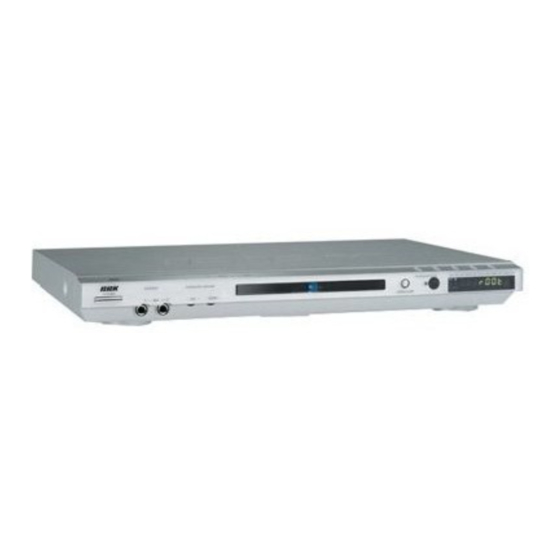
ECHO 11 12 POWER switch STOP button MIC VOLUME knob Disc tray ECHO adjustment knob REV button OPEN/CLOSE button FWD button IR SENSOR MIC 1 jack LED display window PLAY button Headphone jack MIC 2 jack PAUSE button... -
Page 5: Prevertion Of Static Electricity Discharge
4.PREVENTION OF STATIC ELECTRICITY DISCHARGE The laser diode in the traverse unit (optical pickup)may brake down due to static electricity of clothes or human body. Use due caution to electrostatic breakdown when servicing and handling the laser diode. 4.1.Grounding for electrostatic breakdown prevention Some devices such as the DVD player use the optical pickup(laser diode)and the optical pickup will be damaged by static electricity in the working environment.Proceed servicing works under the working environment where grounding works is completed. -
Page 6: Assembling And Disassembling The Mechanism Unit
5. Assembling and disassembling the mechanism unit 5.1 Optical pickup Unit Explosed View and Part List Pic (1) - Page 7 Materials to Pic (1) PARTS CODE PARTS NAME Q ty 14692200 SF-HD60 1EA0311A06300 ASSY, CHASSIS, COMPLETE 1EA0M10A15500 ASSY, MOTOR, SLED 1EA0M10A15501 ASSY, MOTOR, SLED 1EA2451A24700 HOLDER, SHAFT 1EA2511A29100 GEAR, RACK 1EA2511A29200 GEAR, DRIVE 1EA2511A29300 GEAR, MIDDLE, A 1EA2511A29400 GEAR, MIDDLE, B 1EA2744A03000 SHAFT, SLIDE 1EA2744A03100...
-
Page 8: Bracket Explosed View And Part List
5.2 Bracket Explosed View and Part List Pic (2) Materials to Pic(2) 1.bracket 14. front silicon rubber 2.belt 15. Back silicon rubber 3.screw 16. Pick-up 4.belt wheel 17. Pick-up 5.gearwheel 18. switch 6.iron chip 19. Five-pin flat plug 7. Immobility mechanism equipment 20. -
Page 9: Miscellaneous
5.3 MISCELLANEOUS 5.3.1 Protection of the LD(Laser diode) Short the parts of LD circuit pattern by soldering. 5.3.2 Cautions on assembly and adjustment Make sure that the workbenches,jigs,tips,tips of soldering irons and measuring instruments are grounded,and that personnel wear wrist straps for ground. Open the LD short lands quickly with a soldering iron after a circuit is connected. -
Page 10: Electrical Confirmation
6.Electrical Confirmation 6.1. Video Output (Luminance Signal) Confirmation DO this confirmation after replacing a P.C.B. Measurement point Mode Disc Color bar 75% DVDT-S15 Video output terminal PLAY(Title 46):DVDT-S15 PLAY(Title 12):DVDT-S01 DVDT-S01 Measuring equipment,tools Confirmation value 200mV/dir,10 sec/dir 1000mVp-p±30mV Purpose:To maintain video signal output compatibility. 1.Connect the oscilloscope to the video output terminal and terminate at 75 ohms. -
Page 11: Video Output(Chrominance Signal) Confirmation
6.2 Video Output(Chrominance Signal) Confirmation Do the confirmation after replacing P.C.B. Measurement point Mode Disc Color bar 75% DVDT-S15 Video output terminal PLAY(Title 46):DVDT-S15 PLAY(Title 12):DVDT-S01 DVDT-S01 Measuring equipment,tools Confirmation value Screwdriver,Oscilloscope 200mV/dir,10 sec/dir 621mVp-p±30mV Purpose:To maintain video signal output compatibility. 1.Connect the oscilloscope to the video output terminal and terminate at 75 ohme. -
Page 12: Mpeg Board Check Waveform
7.MPEG BOARD CHECK WAVEFORM 7.1 27MHz WAVEFORM DIAGRAM 7.2 IC5L0380R PIN.2 WAVEFORM DIAGRAM... -
Page 13: Hy29Lv800
HY29LV800 8 Mbit (1M x 8/512K x 16) Low Voltage Flash Memory 8. HY29LV800 KEY FEATURES Single Power Supply Operation Minimum 100,000 Write Cycles per Sector – Read, program and erase operations from Compatible With JEDEC standards – Pinout and software compatible with 2.7 to 3.6 volts –... - Page 14 HY29LV800 GENERAL DESCRIPTION The HY29LV800 is an 8 Mbit, 3 volt-only, CMOS the memory array, while Temporary Sector Un- Flash memory organized as 1,048,576 (1M) bytes protect allows in-system erasure and code or 524,288 (512K) words that is available in 44- changes in previously protected sectors.
-
Page 15: Block Diagram
HY29LV800 BLOCK DIAGRAM DQ[15:0] A[18:0], A-1 STATE C O N T R O L ERASE VOLTAGE I/O BUFFERS G E N E R A T O R A N D DQ[15:0] S E C T O R S W I T C H E S C O M M A N D W E # REGISTER... - Page 16 HY29LV800 PIN CONFIGURATIONS RY/BY# RESET# W E # BYTE# DQ15/A-1 DQ14 DQ13 DQ12 W E # Standard BYTE# RESET# DQ11 TSOP48 DQ15/A-1 RY/BY# DQ10 DQ14 DQ13 DQ10 DQ12 DQ11 BYTE# DQ15/A-1 DQ14 DQ13 DQ12 W E # Reverse RESET# DQ11 TSOP48 RY/BY# DQ10...
- Page 17 IC42S16101 512K x 16 Bits x 2 Banks (16-MBIT) SYNCHRONOUS DYNAMIC RAM FEATURES DESCRIPTION ICSI 's 16Mb Synchronous DRAM IC42S16101 is organized • Drive Strength for low capacitive bus loading as a 524,288-word x 16-bit x 2-bank for improved • Clock frequency: 166, 143, 125 MHz performance.
-
Page 18: Ic42S16101
IC42S16101 PIN FUNCTIONS Pin No. Symbol Type Function (In Detail) 20 to 24 A0-A10 Input Pin A0 to A10 are address inputs. A0-A10 are used as row address inputs during active 27 to 32 command input and A0-A7 as column address inputs during read or write command input. - Page 19 IC42S16101 FUNCTIONAL BLOCK DIAGRAM COMMAND MEMORY CELL DECODER ARRAY & ADDRESS 2048 CLOCK BUFFER MODE BANK 0 GENERATOR REGISTER DATA IN SENSE AMP I/O GATE BUFFER SELF I/O 0-15 REFRESH COLUMN DECODER REFRESH CONTROLLER CONTROLLER DATA OUT REFRESH SENSE AMP I/O GATE BUFFER COUNTER MEMORY CELL...
- Page 20 8.2 MT1389 MT1389 Progressive-Scan DVD Player SOC Specifications are subject to change without notice MediaTek MT1389 is a DVD player system-on-chip (SOC) which incorporates advanced features like high quality TV encoder and state-of-art de-interlace processing. The MT1389 enables consumer electronics manufacturers to build high quality, cost-effective DVD players, portable DVD players or any other home entertainment audio/video devices.
-
Page 21: Mt1389
MT1389 PRELIMINARY, SUBJECT TO CHANGE WITHOUT NOTICE MTK CONFIDENTIAL, NO DISCLOSURE General Feature List 1024-bytes on-chip RAM Super Integration DVD player single chip Up to 4M bytes FLASH-programming interface High performance analog RF amplifier Supports 5/3.3-Volt. FLASH interface Servo controller and data channel processing Supports power-down mode MPEG-1/MPEG-2/JPEG video Supports additional serial port... - Page 22 MT1389 PRELIMINARY, SUBJECT TO CHANGE WITHOUT NOTICE MTK CONFIDENTIAL, NO DISCLOSURE Audio Effect Processing TV Encoder Dolby Digital (AC-3)/EX decoding Six 108MHz/12bit DACs DTS/DTS-ES decoding Support NTSC, PAL-BDGHINM, PAL-60 MLP decoding for DVD-Audio Support 525p, 625p progressive TV format MPEG-1 layer 1/layer 2 audio decoding Automatically turn off unconnected channels MPEG-2 layer1/layer2 2-channel audio Support PC monitor (VGA)
-
Page 23: Schematic & Pcb Wiring Diagram
9. SCHEMATIC & PCB WIRING DIAGRAM FRONT SCHEMATIC DIAGRAM... - Page 24 FRONT SCHEMATIC DIAGRAM...
- Page 25 POWER BOARD SCHEMATIC DIAGRAM...
- Page 26 POWER BOARD SCHEMATIC DIAGRAM...
- Page 27 OUTPUT BOARD SCHEMATIC DIAGRAM...
- Page 28 OUTPUT BOARD SCHEMATIC DIAGRAM...
- Page 29 OK SUBSIDIARY BOARD...
- Page 30 OK SUBSIDIARY BOARD...
- Page 31 SUBSIDIARY BOARD 1...
- Page 32 SUBSIDIARY BOARD 2...
- Page 35 MIAN SCHEMATIC DIAGRAM...
- Page 36 MIAN SCHEMATIC DIAGRAM MIAN SCHEMATIC DIAGRAM...
- Page 37 MIAN SCHEMATIC DIAGRAM MIAN SCHEMATIC DIAGRAM...
- Page 38 MIAN SCHEMATIC DIAGRAM...
-
Page 39: Spare Parts List
10. SPARE PARTS LIST DV323S MATERIAL LIST 1. MAIN PANEL MATERIAL CODE MATERIAL NAME SPECIFICATIONS UNIT UANTIT LOCATION CONNECT DISPLAY 5231783 SOFT SPONGE SPACER 16×8×4 DOUBLE-FACED HARD SCREEN AND PANEL PCB 0260206 CD11C 10V100U±20%5×7 2 TC401,TC402,TC403 1200415 DISPLAY SCREEN LTG-0275G... - Page 40 0880581 TL431C TO-226AA(LP) U503 0880800 431L TO-92 U503 0880888 KA431AZ TO-92 U503 1000004 POWER GRID FILTER UT-20 40mH ±20% 10×13 L501 PHOTOELECTRIC 1080011 HS817 U502 COUPLER 0880379 LM7805 GOLD SEALED TO-220 U504 1562710 5934S-0 1940029 SOCKET 9P 2.5mm CN503 1940001 SOCKET 2P 2.5mm CN502...
- Page 41 1562556 B963A-1 1. OK BOARD P MATERIAL CODE MATERIAL NAME SPECIFICATIONS UNIT UANTIT LOCATION CARBON FILM RESISTOR 1/6W560Ω±5% R603,R604 0090014 SMD RESISTOR 1/16W 1K ±5% R607,R608,R619 0000022 CARBON FILM RESISTOR 1/6W1K±5% R611,R626 0000133 CARBON FILM RESISTOR 1/6W4.7K±5% SHAPED 7.5 R622,R628 0090020 SMD RESISTOR 1/16W 5.1K ±5%...
- Page 42 1910095 TERMINAL SOCKET AV1-8.4-5G-2 BLACK JK704 1910006 TERMINAL SOCKET S-VIDEO JK703 1940024 SOCKET 5P 2.0mm XS702 1563578 7323S-0 2100010 CONNECTION CORDS Φ0.6 SHAPED 5mm JP701~JP706 2100003 CONNECTION CORDS Φ0.6 SHAPED 7.5mm JP707£ ¬ JP07 2100004 CONNECTION CORDS Φ0.6 SHAPED 10mm R707,L713,L714 1.
- Page 43 0090609 PRECISION SMD RESISTOR 1/16W 100Ω ±1% 0603 R243 0090626 PRECISION SMD RESISTOR 1/16W 200Ω±1% 0603 R242 0090319 PRECISION SMD RESISTOR 1/16W 750K ±1% 0603 R227 R224,R246,R252,R308,R310, 0090034 SMD RESISTOR 1/16W 100K ±5% 0603 R2111,R2112 SMD RESISTOR 0100019 1/16W33Ω ±5% 8P RN209,RN210 NETWORKS SMD RESISTOR...
- Page 44 VD201,VD205~VD207,VD21 0700002 SMD DIODE LL4148 0~VD221 07800509 TRIODE S8050D V307,V308 07800499 TRIODE S8550D V306,V309 0780062 SMD TRIODE 9014C V310 0780063 SMD TRIODE 9015C Q204 780197 SMD TRIODE C1815 Q205,Q206,Q212 0780198 SMD TRIODE 2SA1015 Q211,Q218,Q219 0780040 SMD TRIODE 3904 V305 0780193 SMD TRIODE 2SK3018 V303,V304...
Need help?
Do you have a question about the DV323S and is the answer not in the manual?
Questions and answers