LG CED-8083B Service Manual
Hide thumbs
Also See for CED-8083B:
- Owner's manual (27 pages) ,
- Manual del usuario (27 pages) ,
- Owner's manual (23 pages)
Table of Contents
Advertisement
Quick Links
This service manual provides a variety of service
information.
It contains the mechanical structure of the CD-
R/RW Drive and the electronic circuits in
schematic form. This CD-R/RW Drive was
manufactured and assembled under our strict
quality control standards and meets or exceeds
industry specifications and standards.
This CD-R/RW drive is an internal drive unit
designed for use with IBM PC, HP Vectra, or
1. General
1) Enhanced IDE interface.
2) Internal 5.25 inch, halfheight CD-R/RW Drive.
3) 2 Mbytes buffer memory.
4) Audio CD like tray loading of a disc without using a caddy.
5) Power loading and power ejecting of a disc. The disc can also be ejected manually.
6) Supports Power saving mode and Sleep mode.
7) Vertical and Horizontal operation.
2. Supported disc formats
1) Reads and writes data in each CD-ROM, CD-ROMXA, CD-I FMV, Video CD, and CD-EXTRA
2) Reads data in Photo CD (Single and Multi session).
3) Reads and writes standard CD-DA.
4) Reads and writes CD-R discs conforming to "Orange Book Part 2".
5) Reads and writes CD-RW discs conforming to "Orange Book Parts 3".
3. Supported write method
1) Disc at once (DAO), Session at once (SAO), Track at once (TAO), Variable packet, Fixed packet, and
Multi-session.
4. Performance
1) Random 100 ms average access time.
2) Max 4,800 kB/sec (Max 32X) Sustained Transfer rate.
3) Supports real time error correction and real time layered error correction at each speed.
4) Supports CD-R write operation at double speed, quadruple speed, and eight speed.
5) Supports CD-RW write operation at double speed and quadruple speed.
6) PIO Mode 4 & Multi DMA Mode 2 Support.
7) MPC-3 Spec compliant.
5. Audio
1) Output 16 bit digital data over ATA interface.
2) 4 Times Digital Filter for CD Audio
3) Software Volume Control
4) Equipped with audio line output and headphone jack for audio CD playback.
5) Front panel Volume Control for Headphone Output.
INTRODUCTION
compatible computer. It can write as much as 650
Mbytes of digital data into CD-R/RW disc, and can
read as much as 650 Mbytes of digital data stored
in a CD-ROM, CD-R and CD-RW disc.
This CD-R/RW Drive can easily meet the
upcoming MPC level 3 specification, and its
Enhanced Intelligent Device Electronics (E-IDE)
and ATAPI interface allows Plug and play
integration in the majority of today's PCs without
the need of an additional interface card.
FEATURES
3
Advertisement
Table of Contents

Related Manuals for LG CED-8083B


Summary of Contents for LG CED-8083B
- Page 1 INTRODUCTION compatible computer. It can write as much as 650 This service manual provides a variety of service Mbytes of digital data into CD-R/RW disc, and can information. read as much as 650 Mbytes of digital data stored It contains the mechanical structure of the CD- in a CD-ROM, CD-R and CD-RW disc.
-
Page 2: System Requirements
SPECIFICATIONS 1. SYSTEM REQUIREMENTS -CPU: IBM Compatible Pentium 233MHZ (or faster) (For 8X Write speed, 266MHz or faster recommended.) -32MB Memory or greater 2. SUPPORTING OPERATING SYSTEM • DOS 3.1 or Higher • Solaris Ver 2.4 or higher • Windows ‘95/’98 •... -
Page 3: Power Requirements
47 kΩ Response + 20 % at 32 Ω 0.6Vrms 1KHz 0dB No Filter H/P Volume MAX Output Level * CED-8080B/CED-8083B DIFFERENCES TABLE MODEL Funtion CED-8080B CED-8083B • CD-R Writing speed 2x/4x/8x Data writing 2x/4x Data writing • CD-RW Writing speed... -
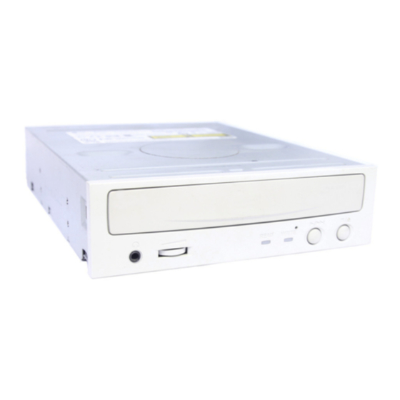
Page 4: Location Of Customer Controls
LOCATION OF CUSTOMER CONTROLS Front Panel Disc Tray Stop/Eject Button Play/Skip Button Volume Control Drive Activity Indicators Headphone Jack 1. Disc tray 4. Volume control This is the tray for the disc. Place the disc on the This is used to adjust the output volume of the ejected disc tray, then lightly push the tray (or headphone jack. -
Page 5: Rear Panel
Rear Panel Analog Audio Output Connector IDE Interface Connector Jumper Connector Power Connector Digital Audio Output Connector 1. Power Connector 3. Jumper Connector Connects to the power supply (5-and 12-V DC) of This jumper determines whether the drive is the host computer. configured as a master or slave. -
Page 6: Cabinet And Circuit Board Disassembly
DISASSEMBLY 1. CABINET and CIRCUIT BOARD 1-3. Cabinet and Main Circuit Board A. Remove the Cabinet in the direction of arrow (4). DISASSEMBLY (See Fig. 1-3) 1-1. Bottom Chassis B. Release 2 hooks (a) and remove the CD Tray A. Release 4 screws (A) and remove the Bottom Chassis drawing forward. -
Page 7: Sled Motor Assy
2-2. Pick-up A. Release 1 screw (C) and remove the Pick-up. Pick-up Unit Pick-up Fig. 1-5 2-3. Sled Motor Assy A. Release 2 screws (D),(E) and remove the Sled Motor Assy. Sled Motor Assy (D) (E) Fig. 1-6... -
Page 8: Troubleshooting Guide
TROUBLESHOOTING GUIDE Reset or Power Check. Check it after connecting the power cable only on interface cable for NO Reset or Power ON. Are the pin 41 • Check the power(12V, 5V) short. and 44 of PN201 +12V and +5V •... - Page 9 System Check. Load tray without inserting disc. Does Tray operate normally? Go to “Tray operating is abnormal” Go to “Sled operating is abnormal” Does Pick-up move to inside? Does Spindle Motor Go to “Spindle operating is rotate in a moment? abnormal”...
- Page 10 Tray operating is abnormal. (Tray open/close doesn’t work) Is the input voltage • Check the connection of IC201 pin 52. 0V at IC301 pin 52 when push the • Replace the SW802(Eject s/w) SW802? • Check the connection of IC409 pin 12. •...
- Page 11 Sled operating is abnormal. Is there Sled Check the connection of IC301 pin 85 Replace the IC301 (MICOM). control signal output? (IC301 pin 85) Is there Sled drive voltage • Check the connction of IC502 pin 17. input? (IC501 pin 23) •...
- Page 12 Spindle operating is abnormal Is there Is there • Check the connection of IC201 pin 2. DMO signal input? Spindle control signal input? • Replace the IC201(OTI-9790). (IC509 pin 5) (IC510 pin 22) Is there Spindle • Replace the IC509(NJM3404). control signal output? (IC509 pin 7) Replace the IC508(BU4053).
- Page 13 Focus Actuator operating is abnormal • Check the connection of IC201 pin 207. Is there Focus • Check the communication line between Search control signal input? IC201 and IC301. (IC501 pin 3) • Replace the IC201 (OTI-9790) • Is there Focus Check the connection of IC301 pin Is Act_Mute signal “L”? Search drive voltage output?
- Page 14 Spindle control is abnormal 2 (CD-ROM Disc) Is there RRF signal input? Go to “RF output is abnormal” (IC413 pin 3) Is there RFDC signal input? Replace the IC413(EL2245). (IC401 pin 85) Does Tracking Servo Go to “Track Servo is unstable” operate normally? Go to “Disc recognition is abnormal”...
- Page 15 Disc recognition is abnormal Is there RECD1, Is there CDR/RW signal input RECD2 signal output normally? Go to “RF output is abnormal” normally? (IC601 pin 33) (IC401 pin 48, 49) Go to “Track Servo is unstable” Replace IC301 (MICOM) RF output is abnormal Is there PICK UP (A, B, C, D) •...
- Page 16 Focus Servo is unstable Is FE signal output normal in Focusing Check the IC401(CXA2551R). Up/Down? (IC401 pin 56) Go to “RF output is abnormal” Is FAQ signal output normal in Focusing Replace the IC201(OTI-9790) Up/Down? (IC201 pin 207) Go to “Focus Actuator operating is abnormal”...
- Page 17 Laser is abnormal Execute ‘B.Calibration Data’ of ‘How to use Test Tool (Dragon)’ Is EEPROM Data valid? Execute ‘D.LD Inspection’ of ‘How Execute ‘C.LD Power Setup’ of to use Test Tool(Dragon)’ ‘How to use Test Tool(Dragon)’ OFF LEVEL NG? Normal VRDC NG? VWDC1 NG?
- Page 18 PN401 Pin 25(VRDC) : • Check the connection of IC401 pin 13. CED-8080B:0.9 + 0.5V, • Check and replace the IC401. CED-8083B:0.6 + 0.5V? Execute ‘D. LD Inspection’ of ‘How to use Test Tool(Dragon)’ VRDC NG? Check the P/U connector and then Normal...
- Page 19 LD CHECK (Not Recorded) Execute ‘E. LD On’ of ‘How to use Test Tool(Dragon)’: ‘VWDC-1 Loop’ • Check the connector of IC601 pin 20. PN401 Pin 32(ENAB) = ‘H’? • Check and replace the IC601(CPLD). • Check the connection of IC601 pin 18,29 and 34. PN401 Pin 31(W/XR) = ‘H’? •...
- Page 20 PN401 Pin 31(W/XR) = ‘H’? • Check and replace the IC601(CPLD). PN401 Pin 26(VWDC2) : • Check the connection of IC409 pin 19. CED-8080B:3.4 + 0.4V, • Check and replace the IC409(DAC). CED-8083B:2.5 + 0.4V? Check the P/U connector and replace the P/U.
- Page 21 Does the disc if the disc has long width have any Dust, Scratch, Scratch, change it. Fingerprint...? Use LG bundle Software (Write Tool & Version) Is the write Tool(version) - Easy CD Creator 3.5c supported by LG CD-RW Direct CD 2.5d...
- Page 22 Writing Part Check. Refer “Laser is abnormal”. Load tray with CD-R/RW Disc. Run the Writing Tool (Easy CD Creator). Run the Writing with Tool (Easy CD Creator). The blink Do the IC301(MICOM) alternates between LED1 and pin 2 and pin 7 output toggle LED2 when Writing start (OPC signals during Writing? operation)?
- Page 23 ALPC Logic Circuit Check. Execute ‘E. LD On’ of ‘How to use Test Tool(Dragon)’ : ‘CD-R Recording Mode’ • Check the connection of IC301 pin 20. IC601 Pin 33 (CDR/RW) = ‘H’? • Check and replace the IC301. • Check the connection of IC301 pin 14. IC601 Pin 34(WR/RE) = ‘H’? •...
- Page 24 Execute ‘E. LD On’ of ‘How to use Test Tool (Dragon)’ : ‘CD-RW Recording Mode’ • Check the connection of IC301 pin 20. IC601 Pin 33(CDR/RW): ‘L’? • Check and replace the IC301. • Check the connection of IC301 pin 14. IC601 Pin 34 (WR/RE) : ‘H’? •...
- Page 25 BETA Measurement Circuit Check. After inserting Test Disc (TCD-784), 1x play. • Check the connection of IC401 pin 86. IC401 Pin 86(RRF) : 3+/-1.0V? • Check and replace the IC401(CXA2551R). • Check the connection of IC407. RRFIN: 2+/0.7V? • Check and replace the IC407. (IC401 PIN85) •...
- Page 26 No audio output Insert the audio Disc. AUD_MUTE : ‘L’? • Check and replace the IC301. (IC301 Pin 8) Do LOUT, ROUT signals output? • Check and replace the IC201. (IC201 Pin 151, 154) Do audio Line signals output? • Check the connection of L/R OUT.
- Page 27 In case of audio play switch not working. • Check the connection of IC301 pin51. Is IC301 pin 51 5V before pushing • Replace the IC301. PLAY KEY (SW801)? • Check the connection of SW801. Is IC301 Pin 51 0V pushing •...
- Page 28 GLOSSARY ATIP Absolute Time in Pre-groove. With an additional modulation of the “Wobble”, the “Groove” contains a time code information. Wobble The pre-groove in the Disc is not a perfect spiral but is wobbled. With : – A typical amplitude of 30 nm –...
-
Page 29: The Differences Of Cd-R/Cd-Rw Discs And General Cd-Rom
The differences of CD-R/CD-RW discs and General CD-ROM 1. Recording Layer Recordable CD has a wobbled pre-groove on the surface of disc for laser beam to follow track. Track pitch(p) a=30nm Read-only Disc CD-ROM (READ-ONLY DISC) Radial Direction Radial Error Signal 0.4~0.5 um Groove Land... -
Page 30: Disc Materials
3. Disc Materials 1) CD-ROM disc • It is composed of Silver _ colored aluminum plate and Reflective layer. • Groove (Pit) of aluminum plate make a track. • Laser wavelength : 780 nm, Laser Power (Read): 0.5mW • Signal is detected by the difference of reflective beam intensity between “pit”... -
Page 31: Reading Process Of Optical Disc
3) CD-RW Disc Label Printing Protective Layer Dielectric Layer(TL) Reflective Layer Dielectric Layer(UL) Substrate (Polycarbonate) Groove Laser Beam • It is composed of polycarbonate layer, alloy(silver, arsenic) layer, aluminum reflectivity layer, protective layer. • An crystalized alloy layer is transformed into noncrystalized by the laser heat. Therefore, writing and reading is enabled by the difference of reflectivity. -
Page 32: Writing Process Of Cd-R Disc
5. Writing Process of CD-R Disc Incident (Write) Laser Power (Read) (Read) Laser Spot a b c d e f Position (Time) Laser Below "ORP"– Mark Too Short Spot Reflected At Optimum Record Power ("ORP") Light Signal Above "ORP" – Mark Too Long Recorded Mark Time... - Page 33 7. Organization of the PCA, PMA and Lead-in Area 1) Layout of CD-ROM disc Disc Center Diameter 120 mm Diameter 46 mm Diameter 15 mm Center hole Clamping and Label Area Information Area Read Only Disc Lead-in Area Program Area Lead-out Area 2) Layout of CD-R/RW disc Disc Center...
-
Page 34: Function Of Pca And Pma Area
8. Function of PCA and PMA area 1) PCA (Power Calibration Area) • PCA area is used to determine the correct Laser Power for a disc. – Method 1 : PCA area is divided by a track. – Method 2 : The previous Calibration value is referred. –... -
Page 35: Writing Process Of Disc
2) ROPC (Running Optimum Power Control) • Variable primary factor of Optimum Power – Change of Power sensitivity on the Disc. (limited to 0.05 *Po) – Wavelength shift of the laser diode due to the operating temperature change. – Change of the Spot aberration due to the Disc skew, Substrate thickness, Defocus. -
Page 36: Internal Structure Of The Pick-Up
INTERNAL STRUCTURE OF THE PICK-UP 1. Connection diagram of the Pick-up *KRS-202A : CED-8080B’S *KRS-220C : CED-8083B’S 2 Axis Actuator FCS - TRK - TRK + FCS + FGND PDGND PDVcc PDVc FPDVc FPDO CFREQ CMOD PGND VRDC Q1 S... -
Page 37: Pin Description
2. Pin Description Pin No. Symbol Function FCS- Focus coil- TRK- Tracking coil- TRK+ Tracking coil + FCS+ Focus coil + FGND Frame GND PGND PDIC GND PDIC F OUT PDIC B OUT PDIC A OUT PDIC H OUT PDIC VCC PDIC VC PDIC G OUT PDIC D OUT... -
Page 38: Signal Detection Of The P/U
3. Signal detection of the P/U Infrared Iaser Pick-Up module Focusing Tracking Photo Diode 1) Focus Error Signal ==> (A+C)-(B+D) This signal is generated in RF IC (IC401 : CXA2551R) and controls the pick-up’s up and down to focus on Disc. -
Page 39: Description Of Circuit
DESCRIPTION OF CIRCUIT 1. ALPC (Automatic Laser Power Control) Circuit 1-1. ALPC Loop Circuit... - Page 40 1-2. ALPC (Automatic Laser Power Control) Circuit Operation This circuit consists of Feedback Loop to maintain light output of the Laser Diode. Feedback signal, output current from PD (Photo Detector) of P/U, is used to monitor the light power of Laser Diode.
- Page 41 2. RF Amplifier Circuit Block Diagram...
-
Page 42: Focus/Tracking/Sled Servo Circuit
3. Focus/Tracking/Sled Servo Circuit 3-1. Focus, Tracking & Sled Servo Process Focus, Tracking Serve IC401 CXA2551R Pick up A,B,C,D,E,F,G,H A,B,C,D Focus Error Detector A,B,C,D Track Error Detector E,F,G,H Focus, Tracking Actuator IC201 IC501 Servo control Driver OTI9790 BA5983FM Level shift Digital EQ Auto Adj. -
Page 43: Focus Servo
3-2. Focus Servo The aim of Focus Servo is to maintain the distance between object lens of P/U and disc surface, so that the detected RF signals (A, B, C, D) can be maximized. Focus Servo is based on focus error (FE) signal which is generated from focus error detection block in CXA2551R (IC401) using Astigmatism Method. -
Page 44: Spindle Servo Circuit
4. Spindle Servo Circuit 4-1. Spindle Servo Process Spindle Servo Process Pick up IC401 CXA2551 Wobble Signal Generator IC201 OTi9790 Spindle Motor PLL BLOCK CD EFM CLV CAV x32 Hall sensor IC201 OTi9790 Wobble Signal IC510 Demodulation BA6664FM ATIP CLV, FG ATIP CLV Control IC509 NJM3404AV... - Page 45 1. Install CED-8080B(CED-8083B) –> PC Power ON –> Execute Windows. 2. Execute Dragon.exe on Windows (Dragon.exe & dragon.cfg should be on same Directory). 3. If you use CED-8080B(CED-8083B) “E4 Dragon Ver xxx(E5 Dragon Ver xxx)” will be displayed on the Window. 4. Select Setup/Setup I/F on the menu bar.
- Page 46 C. LD Power Setup (VWDC1 / VWDC2 re-setup) 1. Remove disc on the tray. 2. Select LD Inspection/Laser Power Setup on the menu bar, and then Laser Power Setup window will appear in sight. 3. Setup LD Power meter (Frequency : 780nm, Measure Range : 0.01mW unit).
- Page 47 E.LD On 1. Remove disc on the Tray. 2. Select LD Inspection/LD ON on the menu bar, and then Laser On window will appear. 3. Select LD ON Mode and Click On button, then LD On. 4. Execute Test (Measure LD Power). 5.
-
Page 48: Major Ic Internal Block Diagram And Pin Description
MAJOR IC INTERNAL BLOCK DIAGRAM AND PIN DESCRIPTION IC401 (CXA2551R) : RF Signal Processor for CD-R/RW Block Diagram 75 74 73 72 71 70 69 68 67 66 65 64 63 62 61 60 59 58 57 56 55 54 53 52 51 BH01 WLDON PHC1... - Page 49 • Pin Description Pin No. Name Pin Description – Center Error Amp Input (+) – Center Error Amp Input (-) Center Error Amp Output SWRF Write RF Servo Signal Output (for Running OPC) WREF Power Sertting Voltage Input for Write APC APCCSW –...
- Page 50 Pin No. Name Pin Description RFPDSH Sample Pulse Input for Read APC WBLSH Sample Pulse Input for Wobble Signal SPDSH Sample Pulse Input for Side Beam Signal MPDSH Sample Pulse Input for Main Beam Signal ROPCSH Sample Pulse Input for Running OPC DGND Digital Ground Pin DVCC...
- Page 51 Pin No. Name Pin Description PHC2 – CAP Connector Pin for RRFIN Signal Peak Hold BHC2 – CAP Connector Pin for RRFIN Signal Bottom Hold RRFIN CAP Connector Pin for RRF Read RF Signal Output MCLK Main Clock Input Write RF Signal Output Main Push–Pull Signal Output Side Beam Signal (H) Input Side Beam Signal (G) Input...
- Page 52 IC201(OTI-9790) : ATAPI Interface, Write and DSP Signal Processor Block Diagram RD[15:0] DPLL OTI-9790 ROE# VPSET CIRC RCASL# Register RCASH# MONIT DRAM RWE# DEFS EFMR3 Interface EFMR2 RRAS0# Subcode DSFS Decoder 4K SRAM EFMR1 RA11/RRAS1# Interface SUBIN RA10/RRAS2# SUBCK RA9/RRAS3# PANICIN ESFS CIRC...
- Page 53 • Pin Description Clock Pin No. Pin Name Type Description Crystal In : System Clock (33.8688MHz) XOUT Crystal Out: System Clock CLKOUT Clock Output C34M Set to 34.5744MHz CD ENCODER/DECODER Interface Pin No. Pin Name Type Description PANICIN Panic Input : Write abort Input WBLIN Wobble In : Wobble Input–Digital Signal HFSW...
- Page 54 CD-SERVO Interface Pin No. Pin Name Type Description Spindle Motor Servo Output Sled Servo Output Focus Servo Output : Focus servo feedback signal Tracking Servo Output : Tracking servo feedback signal TEBC Tracking Error Balance Control Focus Error Tracking Error Beam Strength : This input from the preamplifier is the sum of the E and F photodiode outputs when using a 3-beam pick-up RPBC...
- Page 55 AUDIO Interface Pin No. Pin Name Type Description MIO0 Multi Purpose I/O MIO1 Multi Purpose I/O MIO2 Multi Purpose I/O DOUT Digital Audio Output : Bi-phase serial audio output that follows the EIAJ CP1201 standard. MIO3 Multi Purpose I/O Left Channel Audio Output Right Channel Audio Output Note: MIO3-0 can be programmed to control an external audio DAC.
- Page 56 Pin No. Pin Name Type Description DMACK# ATA DMA Acknowledge/DMA Request : ATAPI DMA acknowledge DMA request when connected to SCSI controller IORDY/ DDMARDY#/ ATA Host I/O Ready : I/O channel ready DSTROBE UDMA : DDMARDY#, device DMA ready; DSTROBE, device data strobe HRD#/ HDMARDY#/ ATA Host Read Strobe/SCSI DMA Read Strobe...
- Page 57 Pin No. Pin Name Type Description Address : Use these pins if the microcontroller has a separate address and data bus. UA15 UA14 UA13 UA12 Address : Use these pins when accessing 64 KB buffer memory window. UA11 UA10 UALE Address Latch Enable : Use this pin if the microcontroller has multiplexed addess and data bus.
- Page 58 Pin No. Pin Name Type Description RAM Data : Data for DRAM Possible to set bus size (16 bit/8bit) by setting internal registers RRAS0# Row Address Strobe 0 : RAS for DRAM RCASH# Column Address Strobe High : CAS0 for DRAM – If 16 bit bus is selected, this pin used by strobe RCASL# Column Address Strobe Low...
- Page 59 IC301 (HD64F3062) : MICOM Block Diagram Port 3 Port 4 Address bus P5 /A Data bus (upper) P5 /A P5 /A Data bus (lower) P5 /A EXTAL P2 /A XTAL P2 /A STBY H8/300H CPU P2 /A P2 /A RESO/FWE* P2 /A P2 /A Interrupt controller...
- Page 60 •Pin Description Port Name Assign Description CS7/TMO0/TP8/PB0 LED2 LED2 control output CS6/TMIO1/TP9/PB1 /PRST OTI9790 Reset control output CS5/TMO2/TP10/PB2 /UCS1 OTI9790 Register Select1 CS4/TMIO3/TP11/PB3 /UCS0 OTI9790 Register Select0 TP12/PB4 ADSEL HALL/Seld Out Select TP13/PB5 LED1 LED1 control output TP14/PB6 AUD_MUTE Audio mute output TP15/PB7 FWE_ON Flash writing enable output...
- Page 61 Port Name Assign Description A14/P26 /PLAY_KEY Play_key input A15/P27 /EJECT_KEY Eject_key input A16/P50 XTOR Tracking error amplitude detection input A17/P51 MA/SL Master / slave detection input A18/P52 TESTMODE1 Test Mode 1 A19/P53 FLAGB OTI9790 FLAGB (RFZC) Input P60/WAIT URDY Data ready input P61/BREQ AGCON Wobble AGC enable output...
- Page 62 IC409(M62352GP) 1) The M62352 is an integrated circuit semiconductor of CMOS structure with 12 channels of built-in D-A converters with output buffer operational amplifiers. 2) Outputs of 12 channels are used for adjustment/control of servo circuits and references. Block Diagram Ao12 Ao11 12-BIT SHIFT REGISTER...
- Page 63 IC501 (BA5983 FM) 1) It controls the sled movement in track search mode and takes the tray to open/close. 2) It controls the Focus/Tracking Actuator receiving the focus error or tracking error signal from IC201. Block Diagram Standby 10K 10K LEVEL SHIFT LEVEL...
- Page 64 IC510 (BA6664FM) : Spindle Motor Drive IC It drives the spindle motor receiving the spindle control signal at IC301 (MICOM) and IC201 (OTI-9790). DRIVER Block Diagram GAIN GAIN SWITCH CONTROL CURRENT SENSE AMP HALL AMP TORQUE SENSE AMP SERVO SIGNAL Hall 1 H2 + CK Q...
- Page 65 IC502 (BA5925FV) It detects the speed of the moving sled, and transfers the sled control signal from IC201 (OTI-9790) to IC501 (BA5983FM) Block Diagram 6.8K EDGE LEVEL SHIFT LOGIC 100K 100K 100K 100K STBY 8.2K 8.2K 8.2K 8.2K • Pin Description Pin No.
- Page 66 BLOCK DIAGRAM 1. Block Diagram of CD-R/RW Drive...
-
Page 67: Power Block Diagram
2. Power Block Diagram... -
Page 68: System Control Block Diagram
3. System Control Block Diagram... - Page 69 4. Write/Read Block Diagram...
- Page 70 5. Block Diagram * CED-8080B : Optical Pick-up KRS-202A * CED-8083B : Optical Pick-up KRS-220C 33.86MHz cable OTI9790 CXA2551R DSP + Servo RF Amp. DECODER Wobble ENCODER ALPC ATIP Demodulator Data Write Strategy *Optical DRAM Disc Pick-up Motor unit KRS-202A/220C...
- Page 71 EXPLODED VIEW PBM00 (MAIN C. B. A)
Need help?
Do you have a question about the CED-8083B and is the answer not in the manual?
Questions and answers