Table of Contents
Advertisement
Quick Links
This service manual provides a variety of service
information. It contains the mechanical structure of
the CD-ROM Drive together with mechanical
adjustments and the electronic circuits in schematic
• Enhanced IDE interface
• Internal 5.25 inch, halfheight CD-ROM Drive
• Fast 100ms Average Access Time
• Supports 1X and 16X Rotational Modes
• Max 2,400KB/sec Sustained Transfer rate
• Photo-CD Multisession Disc Spec compliant
• Multimedia MPC-3 Spec compliant
• Power Disc Loading/Ejection Mechanism
• 1 Way Eject support (Eject Button )
• Closed Enclosure
• Built-in ATAPI Interface Controller
1. SUPPORTED SYSTEM
IBM Compatible 486SX or Above
2. SUPPORTED OS
• MS-DOS Version 3.1 or Higher
• OS/2 Warp (Ver 3.0)
• Windows '95
3. GENERAL PERFORMANCE
• Data Transfer Rate ..........................................................................................Sustained Data Transfer Rate
• Data Buffer Capacity .....................................................................................................................128 kbytes
• Access Time ......................................................................................................1/3 Stroke Average : 100 ms
4. POWER REQUIREMENTS
• Voltage ........................................................................................................................................+5V DC+5%
• Ripple....................................................................................................................................+5V : 100mVp-p
• Current ...........................................................................................+12V : 150mA (Average), 1A (Maximum)
5. AUDIO PERFORMANCE
• Frequency Response....................................................................................................100Hz~20KHz(+3dB)
• S/N Ratio (IHF-A)..............................................................................................85 dB (Typical at 1 KHz 0dB)
• T.H.D. (20K-LPF) .............................................................................................0.05% (Typical at 1 KHz 0dB)
• Channel Separation .................................................................................................................80 dB(Typical)
• Output Voltage (1kHz 0dB) 47KΩ Load ................................................................................0.7 Vrms + 20%
INTRODUCTION
GENERAL FEATURE
SPECIFICATIONS
form. This CD-ROM Drive was manufactured and
assembled under our strict quality control standards
and meets or exceeds industry specifications and
standards.
• Software Volume Control
• 4 Times Digital Filter for CD Audio
• Built-in MODE-1 ECC/EDC
• MTBF 125,000h POH (at 10% Utilization)
• PIO Mode 4 & Multi DMA Mode 2 support
• Horizontal or Vertical Mounting
• Digital audio output
• Digital audio through ATAPI Interface
• Subcode (P-W) through ATAPI Interface
• Spin-down Mode for energy saving
• Solaris Ver 2.4 or Higher
• Linux slackware 2.3
16 Times Speed(max) : 2,400 kbytes/sec
+5V : 400mA (Average), 0.6A (Maximum)
Normal Speed : 150 kbytes/sec
+12V DC+5%
+12V : 100mVp-p
80 dB (Limit at 1 KHz 0dB)
0.15% (Limit at 1 KHz 0dB)
70 dB(Limit)
3
Advertisement
Table of Contents

Related Manuals for LG CRD-8161B


Summary of Contents for LG CRD-8161B
-
Page 1: Specifications
INTRODUCTION This service manual provides a variety of service form. This CD-ROM Drive was manufactured and information. It contains the mechanical structure of assembled under our strict quality control standards the CD-ROM Drive together with mechanical and meets or exceeds industry specifications and adjustments and the electronic circuits in schematic standards. -
Page 2: Location Of Customer Controls
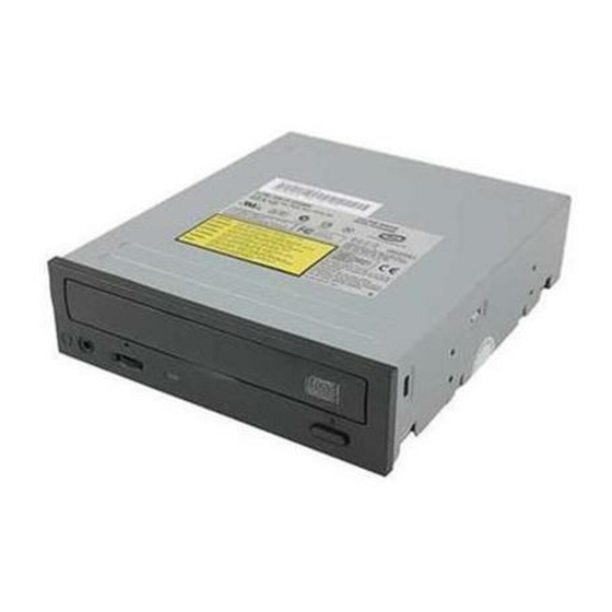
LOCATION OF CUSTOMER CONTROLS FRONT Figure 1. Front View FRONT VIEW Headphone Jack Play/Skip Button 3.5mm jack for monitoring the audio signal from audio When an Audio CD is in the unit, pressing this button CDs. will start playing audio CDs from the first track. If an audio CD is playing, pressing this button will skip to Headphone Volume Control the next track. -
Page 3: Cabinet And Circuit Board Disassembly
DISASSEMBLY 1. CABINET and CIRCUIT BOARD 1-3. Top Case and Chassis Mecha A. Release 2 hooks (a) and remove the Top Case in DISASSEMBLY the direction of arrow (2). 1-1. Bottom Chassis B. Release 4 screws (B) and remove the Chassis A. -
Page 4: Mechanism Assy
2. MECHANISM ASSY 2-2. Pick-Up A. Release 1 screw (G). 2-1. Pick-Up Unit B. Remove the Pick-Up A. Release 1 screw (C). B. Remove the Loading Belt and Loading Gear. C. Release 1 screw (D). D. Remove the stopper (R). E. -
Page 5: Troubleshooting Guide
TROUBLESHOOTING GUIDE 1. Initial Lead-in Operation Reset or Power-On. LED Flikers. Pick-Up moves to the inner-Track. Ratate disc. Laser on the Pick-Up lights. Focus Search (through moving up and down the lens of Pick-Up) Focus Servo On (FOK(TP10) : H, FEO(TP14) signal generation) Tracking Servo On (TEO(TP13) Signal generation) Spindle Servo On (MDP(TP17) Signal generation) Read TOC Area (LED Flikers) - Page 6 3. Troubleshooting Guide (In the Initial Lead-in Operation Mode) Reset or Power On. Check Power Voltage, Reference Electrical Potential and GND. Does “H” output in IC401 Is the CLOCK Frequency Replace Does LED light? of X401 16.93MHz? X401. Check and replace R318, Replace IC401 R323, Q307 and LD301.
- Page 7 Does the Laser (RED Does “H” output in IC102 Replace IC401 light) of Pick-Up light? Is the Voltage of IC102 Replace IC102 (LD) 2.2V? Replace MD Assy (Laser Diode of the Pick-Up is defective.) Does the focus search Does the Pick-Up lens Replace IC203 signal appear between move up and down?
- Page 8 4. Troubleshooting Guide (In the Operation Mode) When the jump is unstable (Noise occurs); (1) Readjust the Slide Motor offset. (2) Replace Main Circuit Board or MD Assy. When the Pick-Up slides to innermost track or outermost track during the Access; (1) Replace MD Assy.
- Page 9 6. Write I/F Signal Flow (Drive << Host) ≈ ≈ ≈ ≈ Dn-3 Dn-2 Dn-1 ≈ ≈ Above figure is timing flow presented data transfer from Host to Drive. And, the followings are those conditions; 1. When the Host write the ATAPI packet command-word 2.
-
Page 10: Block Diagram
IC INTERNAL BLOCK DIAGRAM AND PIN DESCRIPTION IC102 (CXA2556Q) : RF Amplifier IC I-V convertes and amplifies the signal by receiving, from the Pick-up, and than applies to DSP & SSP IC (IC501). Block Diagram BOOST FILTER CONTROL CONTROL CONTROL MODE 1 MODE DELAY... -
Page 11: Pin Description
IC102 CXA2556Q Pin Description Pin No. Symbol Description APC Amp output APC Amp Intput RF Summing Amp, Focus Error Amp Input No Connect Tracking Error Amp Input. (9, 10) Tracking Error Amp Output. (11) Control Tracking Error Low Frequency Gain (12) Tracking Error Amp Output (13) Adjust Focus Bias Focus Error Amp Output... - Page 12 IC201 (BA6849FP) : Spindle Drive IC Controls the Spindle Motor by receiving MDP signal from DSP (IC501). Block Diagram SHORT BRAKE DRIVER CURRENT Vcc2 SENSE AMP GAIN Vcc1 CONTROL Vcc1 HALL AMP TORQUE SENSE AMP SERVO SIGNAL Hall 1 Hall 2 Hall Bias Hall 3 BA6849FP...
- Page 13 IC203 (M56759FP) : Servo Actuator Drive IC Generates the signal to rotate Focus Actuator Coil,Tracking Actuator Coil and Sied Motor by PWM Error Signal input from DSP. Block Diagram 12.5k 2.5k 12.5k 2.5k 12.5k 2.5k 10k 12.5k 12.5k 12.5k 2.5k 2.5k 12.5k 12.5k...
- Page 14 IC401 (M8-3396) : µ-COM Controls all Drive systems by input and output the Data from the peripheral IC. IC501 (CXD3000R) : DSP & SSp Generates Error Signal and return to the Servo by the Signal from RF Amplifier IC. 108 107 106 105 104 103 102 101 100 99 98 97 96 95 94 93 92 91 90 89 88 87 86 85 84 83 82 81 80 79 78 77 76 75 74 73 TESTA DTS2 PWMI...
- Page 15 IC501 CXD3000R Block Diagram 87 6 75 70 28 30 26 78 79 DAC BLOCK AO1F MCKO 4fs Digital Filter AO1R V16M VCKI 1 bit DAC AO2F FSTO AO2R Clock Generator C16M VCTL 32K RAM VCOI VCOO Address Priority Digital PLL generator encoder Vari-Pitch...
- Page 16 IC501 CXD3000R Pin Description Pin No. Symbol Description Slide Error input Focus Error input Center voltage input VPCO1 1, Z, 0 Output of VCO2 charge pump for vari-pitch PLL VPCO2 1, Z, 0 Output 2 of VCO2 charge pump for vari-pitch PLL VCTR Input of VCO2 control voltage for vari-pitch EFM FILO...
- Page 17 Pin No. Symbol Description DA08 1, 0 Outputs DA8 when PSSL=1, or GFS when PSSL=0. DA07 1, 0 Outputs DA7 when PSSL=1, or RFCK when PSSL=0. Digital Power supply DA06 1, 0 Outputs DA6 when PSSL=1, or C2PO when PSSL=0. DA05 1, 0 Outputs DA5 when PSSL=1, or XRAOF when PSSL=0.
- Page 18 Pin No. Symbol Description AO2F 1, 0 CH2•DAC•PWM output Analog power supply Power supply for master clock XTLO 1, 0 X'tal oscillation circuit output of master clock. XTLI X'tal oscillation circuit input of master clock. GND for master clock Analog GND AO1F 1, 0 CH1•DAC•PWM output...
- Page 19 Pin No. Symbol Description TRDR 1, 0 Tracking drive output FFDR 1, 0 Focus drive output FRDR 1, 0 Focus drive output Digital power supply VCOO 1, 0 Output of oscillation circuit analog EFM PLL VCOI Input to oscillation circuit for analog EFM PLL. f =8.6436MHz LOCK TEST...
- Page 20 IC602 (OTI-911LP) : I/F and Decoder IC Applies the order from the PC to µ-COM, and transmittes the input Signal from DSP to PC with Data. Block Diagram RD(7:0) DRAM RAD(15:0) DRAM Control Host/uP HDR/SUBHDR Address Ragisters Counters Host Control CD-DSP Status/Control Address...
- Page 21 IC 602 OTI-911LP Pin Description Pin No. Name Type Comments Pin No. Name Type Comments VSSE uCOM Data Bus RAD3 RAM Address Bus VSSE RAD11 uCOM Data Bus RAD12 uCOM Register Select ALE (RAM Address I/O * ALE/RAD13 URD- uCOM Read Strobe BUS) RAD15 RAM Address Bus...
- Page 22 Pin No. Name Type Comments Pin No. Name Type Comments IDE Host Data Bus RAM Data Bus VSSE VSSE HD13 IDE Host Data Bus RAM Data Bus ARST- ATAPI Reset IDE Host Data Bus RAD10 RAM Address Bus HD12 ROE- RAM Read Enable RAM Data Bus VSSI...
- Page 23 PHOTO DIODE STRUCTURE OF THE PICK-UP Laser spot * C ’=C+D Focus Error Signal => (A+C)-(B+D) (Control the Pick-up’s up and down to focus on the Disc) Tracking Error Signal => (E-F) (Control the Pick-up’s left and right shift to find the track on the Disc) RF Signal =>...
- Page 24 BLOCK DIAGRAM R-CH 33.86MHZ L-CH R-CH L-CH R-CH AUDIO CXD3000R CXA2556Q DSP + SSP CIRCUITARY RF AMP L-CH LASER DISC MOTOR UNIT PICK-UP HEADPHONE (OPTIONAL) SPINDLE SLED LOADINF FOCUS TRACKING MOTOR MOTOR MOTOR COIL COIL I/F CABLE H8/3396 SYSTEM OTI-911LP CONTROLLER DECODER+I/F HOST...
- Page 25 EXPLODED VIEW PBM00 (Main C.B.A)
Need help?
Do you have a question about the CRD-8161B and is the answer not in the manual?
Questions and answers