Table of Contents
Advertisement
Quick Links
Advertisement
Table of Contents

Related Manuals for Akai ADV-73DR


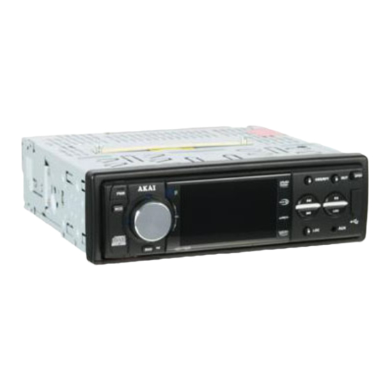
Summary of Contents for Akai ADV-73DR
- Page 2 explode-ASS...
- Page 6 BOTTOMCOPPER...
- Page 8 KB-BOTTOM COPPER...
- Page 9 KB-BOTTOM COPPER...
- Page 10 MB-BOTTOMSILKSCREEN...
- Page 13 KB-TOP COPPER...
- Page 14 KB-TOP SILK...
- Page 15 MB-1...
- Page 16 MB-2...
- Page 17 MB-3...
- Page 20 MB-BOTTOMCOPPER...
- Page 21 MB-BOTTOMVALUE...
- Page 22 MB-TOPVALUE...
- Page 23 TOPCOPPER...
- Page 24 TOPSILKSCREEN...
-
Page 33: Cover Sheet
LTPS LCD Specification... -
Page 34: Table Of Contents
Table of Contents Item Page Cover Sheet Table of Contents Record of Revision Features General Specifications Input / Output Terminals Absolute Maximum Ratings Electrical Characteristics Timing Chart Optical Characteristics Reliability Handling Cautions Mechanical Drawing Packing Drawing... -
Page 35: Record Of Revision
Record of Revision Issued Date Description 0.00 Aug. 21, 2006 New create. Page: 3... -
Page 36: Features
1. FEATURES The 3.0” LCD module is the active matrix color TFT LCD module. LTPS (Low Temperature Poly Silicon) TFT technology is applied with vertical and horizontal drivers built on the panel. Both of horizontal and vertical scan are reversible and controlled by the serial interface commands. The product is designed for the requirement of the green product, and the specification complies with Toppoly’s “Green Product Chemical Substance Specification Standard Hand Book”. -
Page 37: Input / Output Terminals
Recommend connector: Compatible with JAE IL-FHJ-39S-HF-A1 Symbol Description Remark C Capacitor for charge pump C Capacitor for charge pump C Capacitor for charge pump C Capacitor for charge pump C Capacitor for charge pump C Capacitor for charge pump -- No connection PCDL C Capacitor for pre-charge data signal low PCDH... - Page 38 DIN5 Data input DIN6 Data input DIN7 Data input I/O Serial interface data line Serial interface clock line SCEN Serial interface chip enable line SHDB Sleep mode setting pin GRESTB Global reset pin Note 3-1: The figure below shows the connection of backlight LED. Page: 6...
-
Page 39: Absolute Maximum Ratings
Ta = 25 Item Symbol Unit Remark Logic Power Supply Voltage -0.5 VD, HD, DCLK, DIN[0:7], SDA, Input Signal Voltage SCL, SCEN, SHDB, GRESTB Back Light Forward Current Operating Temperature Storage Temperature Page: 7... -
Page 40: Electrical Characteristics
GND=0V, Ta=25 Item Symbol Unit Remark Power Supply Voltage 2.85 Note 5-1 VD, HD, DCLK, Low Level 0.2x Vcc* Input Signal DIN[0:7], SDA, SCL, Voltage SCEN, SHDB, High Level 0.8x Vcc* Vcc* GRESTB PWM Output Voltage Vcc* Feedback Voltage 0.55 0.65 Note 5-2 Panel Power Consumption... -
Page 41: Timing Chart
6. TIMING CHART <Input timing 1> Serial RGBDummy or Serial-YUV 4:2:2 mode --Horizontal-- (1) NTSC Mode: Parameter Symbol Unit DCLK Frequency DCLK Horizontal valid data 1440 DCLK 1 Horizontal Line 1716 DCLK HSYNC Pulse Width DCLK Hsync blanking DCLK Horizontal Front Porch DCLK Horizontal Dummy Time DCLK... - Page 42 (2) PAL Mode: Parameter Symbol Unit DCLK Frequency DCLK Horizontal valid data 1440 DCLK 1 Horizontal Line 1728 DCLK HSYNC Pulse Width DCLK Hsync blanking DCLK Horizontal Front Porch DCLK Horizontal Dummy Time DCLK Parameter Symbol Unit DCLK Frequency 24.38 DCLK Horizontal valid data 1280...
- Page 43 --Vertical-- Interlace: ODD Field: same phase VD and HD EVEN Field: same phase VD and Half-HD Non-interlace: (1) Interlace Mode: NTSC/QVGA Parameter Symbol Unit Vertical valid data 1 Vertical field 262.5 VSYNC Pulse Width DCLK Vsync blanking Odd Field Even Field 21.5 Vertical Front Odd Field...
- Page 44 (2) Interlace Mode: PAL Parameter Symbol Unit Vertical valid data 1 Vertical field 312.5 VSYNC Pulse Width DCLK Vsync blanking Odd Field Even Field 24.5 Vertical Front Odd Field vfpo Porch Even Field vfpe Vertical dummy time (3) Non-Interlace Mode: NTSC/QVGA Parameter Symbol Unit...
- Page 45 <Input timing 2> Through mode --Horizontal- DCLK DIN[7:0] Valid Data Display Area Active Area 1 Horizontal Line(t Parameter Symbol Unit DCLK Frequency 18.42 DCLK Horizontal valid data DCLK 1 Horizontal Line 1171 DCLK HSYNC Pulse Width DCLK Hsync blanking DCLK Hsync front porch DCLK Horizontal dummy time...
- Page 46 --Vertical-- Interlace: ODD Field: same phase VD and HD EVEN Field: same phase VD and Half-HD DIN[7:0] Valid Data Valid Data Display Area Display Area Active Area Active Area vfpe vfpo Odd Field( Even Field( 1 Frame Non-interlace: DIN[7:0] Valid Data Valid Data Display Area Display Area...
- Page 47 (2) Non-Interlace Mode Parameter Symbol Unit Vertical valid data 1 Vertical field Vsync pulse width DCLK Vsync blanking Odd Field Even Field Vsync Odd Field vfpo front porch Even Field vfpe Vertical dummy time Page: 15...
- Page 48 <Input timing 3> Timing Diagram DIN[7:0] DCLK Item Symbol Unit DCLK Duty Ratio Duty Data Setup Time Data Hold Time Control Signal Setup Time Control Signal Hold Time Page: 16...
-
Page 49: Optical Characteristics
7. OPTICAL CHARACTERISTICS 7.1 Optical Specification Ta=25 Item Symbol Condition Unit Remarks Viewing Angles Degree Note 7-1 Contrast Ratio Note 7-2 Rising Response Time Note 7-3 Falling =0° Luminance (I =23mA) cd/m Note 7-4 0.26 0.31 0.36 Chromaticity White Note 7-5 0.28 0.33 0.38... - Page 50 Note 7-1: Viewing angle diagrams: Normal Normal : Viewing Angle : Viewing Angle : Viewing Direction : Viewing Direction 3 O'clock 3 O'clock 3 O'clock 12 O'clock 12 O'clock 12 O'clock 6 O'clock 6 O'clock 6 O'clock =270 =270 =270 9 O'clock 9 O'clock 9 O'clock...
-
Page 51: Reliability
8 REILIABILITY Test Item Condition Ta=+60 , 240hrs High Temperature Operation High Temperature & High Humidity Operation Ta=+40 , 95% RH, 240hrs Ta=-10 , 240hrs Low Temperature Operation Ta=+80 , 240hrs High Temperature Storage (non-operation) Ta=-30 , 240hrs Low Temperature Storage (non-operation) 80 , 50 cycles Thermal Shock (non-operation) 30 min... -
Page 52: Handling Cautions
9 HANDLING CAUTIONS 9.1 ESD (Electrical Static Discharge) Strategy ESD will cause serious damage of the panel, ESD strategy is very important in handling. Fol- lowing items are the recommend ESD strategy (1) In handling LCD panel, please wear non-charged material gloves. And the conduction ring connect wrist to the earth and the conducting shoes to the earth is necessary. -
Page 53: Mechanical Drawing
10 MECHANICAL DRAWING Page: 21... -
Page 54: Packing Drawing
11 Packing Drawing (4). M odule with display face down (1). C ardboard Tray M odule in tray Q 'ty= 1 0pcs (2). Tape E mpty tary = 1Layer C ardboard M odule in tray= 20 Layers C arton (3). D esiccant (5).
Need help?
Do you have a question about the ADV-73DR and is the answer not in the manual?
Questions and answers