
Related Manuals for Advantech PCI-7031


Summary of Contents for Advantech PCI-7031
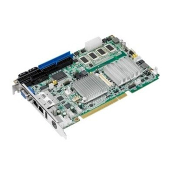
- Page 1 User Manual PCI-7031 ® Intel Atom™ Dual-Core D510/ Fanless N450 CPU, PCI Half-size SBC with on-board DDR2 / VGA / LVDS / Dual-GbE / SATA / COM...
- Page 2 PICMG logos are trademarks of the PCI Industrial Computers Manufacturers Group. All other product names or trademarks are properties of their respective owners. Certifications FCC Class A Part No. 2002703101 Edition 2 Printed in Taiwan December 2009 PCI-7031 User Manual...
- Page 3 In addition, free technical support is available from engineers every busi- ness day. We are always ready to give advice on application requirements or specific information on the installation and operation of any of our products. PCI-7031 User Manual...
- Page 4 It should be free of marks and scratches and in perfect working order upon receipt. As you unpack the PCI-7031, check it for signs of shipping damage. (For example, damaged box, scratches, dents, etc.) If it is damaged or it fails to meet the specifica- tions, notify our service department or your local sales representative immediately.
- Page 5 It should be free of marks and scratches and in perfect working order upon receipt. As you unpack the PCI-7031, check it for signs of shipping damage. (For example, damaged box, scratches, dents, etc.) If it is damaged or it fails to meet the specifica- tions, notify our service department or your local sales representative immediately.
- Page 6 SODIMM Hynix HY5PS121621B FP-Y5 1 GB TS64MSQ64V6M DDR2 (32x16) DDR2 SODIMM 2 GB TS256MSQ64V8U Micron D9HNP (128x8) DDR2 DDR2 SODIMM ELPIDA TWN E5108AHSE-8E- 1 GB DDR2 E (64x8) DDR2 SODIMM ELPIDA JPN E1108ACSE-8E-E 2 GB DDR2 (128x8) PCI-7031 User Manual...
- Page 7 Caution! There is a danger of a new battery exploding if it is incorrectly installed. Do not attempt to recharge, force open, or heat the battery. Replace the battery only with the same or equivalent type recommended by the man- ufacturer. Discard used batteries according to the manufacturer's instructions. PCI-7031 User Manual...
- Page 8 PCI-7031 User Manual viii...
-
Page 9: Table Of Contents
Connecting Peripherals & Jumper Settings ..........11 Introduction ..................... 12 IDE Connector (IDE1) ................12 Figure 2.1 PCI-7031 IDE1 location ..........12 Floppy Drive Connector (FDD1).............. 13 Figure 2.2 PCI-7031 FDD1 location........... 13 Parallel Port (LPT1)................. 14 Figure 2.3 PCI-7031 LPT1 location ........... 14 VGA Connector (VGA1) ................ - Page 10 Exit Options..................... 44 Figure 3.14Exit Options .............. 44 3.8.1 Save Changes and Exit .............. 44 3.8.2 Discard Changes and Exit ............44 3.8.3 Discard Changes ................ 44 3.8.4 Load Optimal Defaults ..............45 3.8.5 Load Failsafe Defaults ..............45 PCI-7031 User Manual...
- Page 11 CPU FAN connector (CPUFAN1) ............71 Table B.8: CPU FAN connector (CPUFAN1)......71 System FAN connector (SYSFAN1) ............71 Table B.9: System FAN connector (SYSFAN1)......71 B.10 Audio Interface Connector (HDAUD1) ............ 72 Table B.10:Audio Interface Connector (HDAUD1)...... 72 PCI-7031 User Manual...
- Page 12 Table B.16:ATX Power Control Connector (ATX1)..... 75 B.17 VGA Connector (VGA1)................75 Table B.17:VGA Connector (VGA1) ........... 75 Appendix C Programming the GPIO ....77 Supported GPIO Register ............... 78 C.1.1 GPIO Registers................78 C.1.2 GPIO Example Program-1............79 PCI-7031 User Manual...
-
Page 13: Chapter 1 Hardware Configuration
Chapter Hardware Configuration... -
Page 14: Introduction
VGA and LVDS dual video outputs also makes it suitable for applications requiring dual display or digital panel display capabilities. PCI-7031 is rich in I/O interfaces: it has three SATA ports (300 MB/sec) for main- stream SSD (solid state disk), HDD, and ODD connections, one legacy IDE port for the ODD connection. -
Page 15: Features
D SKU: Maximum 2 GB DDR2 667 MHz memory in SO-DIMM socket Note! PCI-7031 is ONLY compatible with DDR2 memory modules that are assembled with x16 (16-bit) memory chips and NOT compatible with those that are assembled with x8 (8-bit) memory chips. Using wrong memory modules may cause unexpected system instability. -
Page 16: Input/Output
An on board keyboard pin header connector is also available High Definition Audio: PCI-7031 can provide audio function with the optional audio extension module PCA-AUDIO-HDA1E USB ports: PCI-7031 supports up to 7 USB 2.0 ports with transmission rates up to 480 Mbps 1.3.4 Graphic interface Controller: Integrated graphic core of Embedded Gen3.5+ technology... -
Page 17: Jumpers And Connectors
Board weight: 0.5 kg (1.2 lb) Jumpers and Connectors Connectors on the PCI-7031 single board computer link it to external devices such as hard disk drives and a keyboard. In addition, the board has a number of jumpers used to configure your system for your application. - Page 18 USB port 3 and port 4 pin-header USB 56 USB port 5 and port 6 pin-header USB8 The 7th USB port on rear bracket LANLED1 LAN1 and LAN2 LED connector GPIO1 GPIO header Note! USB7 is reserved and can not be used. PCI-7031 User Manual...
-
Page 19: Board Layout: Jumper And Connector Locations
JFP1 JWDT1 SYSFAN1 LAN12 USB8 CPUFAN1 KBMS1 KBMS2 Note: USB7 is reserved USB1~6 LANLED1 GPIO1 LVDS1 HDAUD1 ATXF1 and can NOT be used. On-board 1GB DDR2 667 Memory (Only on N SKU) LPC1 Figure 1.1 Board Layout PCI-7031 User Manual... -
Page 20: Pci-7031 Block Diagram
Discard used batteries according to manufacturer's instructions. Note! Before installing your PCI-7031 into a chassis, make sure that no com- ponents on either side of the CPU card can touch any metal parts, espe- cially the chassis wall and add-on card in the adjacent slot. -
Page 21: System Memory
System Memory The PCI-7031D has one SO-DIMM socket (while PCI-7031N does NOT). PCI-7031 is ONLY compatible with DDR2 memory modules that are assembled with x16 (16- bit) memory chips and NOT compatible with those that are assembled with x8 (8-bit) memory chips. -
Page 22: Processor Installation
1.10 Processor Installation PCI-7031 series are equipped with soldered-down (BGA type) CPUs. no need for a user to install a CPU. 1.11 CPU Cooler Installation Only PCI-7031D needs to have a CPU cooler installed by user (P/N: 1960046526N001), PCI-7031N does NOT require this; it already has a fanless heat- sink assembled on the CPU card. -
Page 23: Chapter 2 Connecting Peripherals & Jumper Settings
Chapter Connecting Peripherals & Jumper Settings... -
Page 24: Introduction
IDE1 Figure 2.1 PCI-7031 IDE1 location You can attach up to two IDE (Integrated Drive Electronics) drives to the PCI-7031's built-in controller. The primary connector can accommodate two drives. Wire number 1 on the cable is red or blue and the other wires are gray. Connect one end to connector IDE1 on the single board computer. -
Page 25: Floppy Drive Connector (Fdd1)
FDD1 Figure 2.2 PCI-7031 FDD1 location You can attach up to two floppy disk drives to the PCI-7031's on board controller. You can use 3.5" (720 KB, or 1.44 MB) drives. The single board computer comes with a 34-pin daisy-chain drive connector cable. -
Page 26: Parallel Port (Lpt1)
The parallel port is normally used to connect the single board computer to a printer. The PCI-7031 includes an onboard parallel port, accessed through a 26-pin flat-cable connector, LPT1. The card comes with an adapter cable which lets you use a tradi- tional DB-25 connector. -
Page 27: Vga Connector (Vga1)
COMLED1 Figure 2.5 Serial Ports (COM12) The PCI-7031 offers two serial ports: COM1 and COM2. These ports can connect to serial devices, such as a mouse or to a communications network. You may connect the dual COM ports cable kit 1700008762 to COM12 box-header to have these 2 DB9 RS232 ports on the rear bracket. -
Page 28: Ps/2 Keyboard/Mouse Connector (Kbms1)
External Keyboard Pin Header (KBMS2) KBMS2 Figure 2.7 External Keyboard Connector (KBMS2) In addition to the PS/2 mouse/keyboard connector on the PCI-7031's rear plate, there is also an extra onboard external keyboard pin header. This gives system inte- grators greater design flexibility. -
Page 29: Cpu Fan Connectors (Cpufan1)
CPU Fan Connectors (CPUFAN1) CPUFAN1 Figure 2.8 CPU Fan Connectors (CPUFAN1) This connector supplies power and fan speed signal to PCI-7031D's proprietary CPU cooler for Atom D510 CPU. 2.10 Front Panel Connectors (JFP1) Figure 2.9 Front Panel Connectors (JFP1) PCI-7031 User Manual... -
Page 30: Atx Power Button (Jfp1 Pin 1~2)
System On System Suspend Fast flashes Fast flashes Fast flashes System Off Slow flashes 2.10.5 HDD LED (JFP1 Pin 9~10) You can connect an LED to connector (JFP1 Pin 9~10) to indicate when the HDD is active. PCI-7031 User Manual... -
Page 31: Watch Dog Timer (Jwdt1) / Infrared (Jir1)
2.11.1 Watchdog timer output (JWDT1) The PCI-7031 contains a watchdog timer that will reset the CPU in the event the CPU stops processing. This feature means the PCI-7031 will recover from a software fail- ure or an EMI problem. The JWDT1 jumper settings control the outcome of what the computer will do in the event the watchdog timer is tripped. -
Page 32: Dual Giga Lan Rj45 Connector (Lan12)
PCI-7031 uses the Intel 82567V/82583V Gigabit LAN chips are linked to dedicated PCIe x1 lanes. PCI-7031 provide high throughputs for heavy loading networking environment. It provides two RJ-45 connectors in the rear side and is convenient for most industrial applications. -
Page 33: Serial Ata Interface (Sata1 ~ Sata3)
(300MB/Sec) Figure 2.13 Serial ATA interface (SATA1 ~ SATA3) In addition to the EIDE interface (up to two devices), the PCI-7031 features three high performance Serial ATA interfaces (up to 300 MB/s) for easy hard drive cabling with long, thin SATA cables. -
Page 34: Gpio Header (Gpio1)
PCI-7031 provides an external LAN LED pin header for connecting to the front side of the chassis. With this convenient design, users are alerted to LAN port activity. Refer to Appendix B for detailed information on the pin assignments. 2.16... -
Page 35: Cmos Clear (Cmos1)
2.17 CMOS clear (CMOS1) The PCI-7031 single board computer contains a jumper that can erase CMOS data and reset the system BIOS information. Normally this jumper should be set with pins 1-2 closed. If you want to reset the CMOS data, set CMOS1 to 2-3 closed for just a few seconds, and then move the jumper back to 1-2 closed. -
Page 36: Atx Feature Connector(Atxf1)
Important: Make sure that the ATX power supply can take at least a 10mA load on the 5 V standby lead (5 VSB). If not, you may have difficulty powering on your sys- tem. 2.19 ATX power control connector (ATX1) ATX1 PCI-7031 User Manual... -
Page 37: System Fan Connector (Sysfan1)
The PCI-7031 supports ATX power supply. ATX1 supplies main power (+5 V,+12 V, 5 VSB), and it is a 6 x 2 power connector. 2.20 System FAN connector (SYSFAN1) SYSFAN1 The PCI-7031 is equipped with a 3-pin FAN connector providing +12 V power for system FAN. -
Page 38: Usb Ports (Usb 1~6 & 8)
USB8 USB1~6 PCI-7031 supports 7 USB 2.0 ports, you may use the 1700008887 4-port USB cable kit to utilize any four of USB 1~6, USB 8 is located on the rear I/O bracket. USB 7 is reserved and can NOT be used. -
Page 39: Low Pin Count Device Connection Pin Header
PCI-7031 supports a CF card device, an installed CF card will occupy the master IDE device. Please locate it on the solder side of the CPU card. 2.24 Low Pin Count Device Connection Pin Header LPC1 PCI-7031 has a 14-pin female pin header on its solder side to support extension modules. - Page 40 PCI-7031 User Manual...
-
Page 41: Ami Bios Setup
Chapter AMI BIOS Setup... -
Page 42: Figure 3.1 Setup Program Initial Screen
The Setup program uses a number of menus for making changes and turning special features on or off. This chapter describes the basic navigation of the PCI-7031 setup screens. Figure 3.1 Setup Program Initial Screen AMI's BIOS ROM has a built-in Setup program that allows users to modify the basic system configuration. -
Page 43: Entering Setup
Date using the <Arrow> keys. Enter new values through the keyboard. Press the <Tab> key or the <Arrow> keys to move between fields. The date must be entered in MM/DD/YY format. The time must be entered in HH:MM:SS format. PCI-7031 User Manual... -
Page 44: Advanced Bios Features Setup
Advanced BIOS Features Setup Select the Advanced tab from the PCI-7031 setup screen to enter the Advanced BIOS Setup screen. You can select any of the items in the left frame of the screen, such as CPU Configuration, to go to the sub menu for that item. You can display an Advanced BIOS Setup option by highlighting it using the <Arrow>... -
Page 45: Cpu Configuration
Intel® CPU Enhanced Halt (C1E) function, a function to save CPU power con- sumption in system halt state. When enabled, the CPU speed and voltage will be reduced during system halt state to save power consumption. You may choose to enable or disable it. PCI-7031 User Manual... -
Page 46: Ide Configuration
AHCI is a new interface specification that allows the SATA controller driver to support advanced features. While entering setup, BIOS auto detects the pres- ence of AHCI devices. This displays the status of auto detection of AHCI devices. PCI-7031 User Manual... -
Page 47: Super I/O Configuration
This configures parallel port base addresses. The following options are also available: – Parallel Port Mode This option configures Parallel Port mode. Available options include Normal, Bi-directional, ECP, EPP, ECP & EPP. – Parallel Port IRQ This option configures s Parallel Port base IRQ. PCI-7031 User Manual... -
Page 48: Hardware Health Function
ACPI Shut Down Temperature This potion allows user to set the CPU temperature at that the system will auto- matically shut down for preventing CPU from over heat damage. PCI-7031 User Manual... -
Page 49: Apm Configuration
Available options include Power Off, Power On, Last Status. Resume On Ring Disable/Enable RI wake event. Resume On LAN Disable/Enable LAN wake event. Resume On PME Disable/Enable PCIe device PME wake event. Resume On RTC Alarm Disable/Enable RTC wake event. PCI-7031 User Manual... -
Page 50: Pci/Pnp Setup
PCI/PNP Setup Select the PCI/PnP tab from the PCI-7031 setup screen to enter the Plug and Play BIOS Setup screen. Highlighting a Plug and Play BIOS Setup option by using the <Arrow> keys displays a description in the righthand panel. All Plug and Play BIOS Setup options are described in this section. -
Page 51: Boot Setup Utility
Select the Power-on state for Numlock. PS/2 Mouse Support Enable or disable PS/2 interface mouse support. Available options include Auto, Enable, Disable. Wait For ‘F1’ If Error Wait for the F1 key to be pressed if an error occurs. PCI-7031 User Manual... -
Page 52: Security Setup
Security Setup Figure 3.11 Password Configuration Select Security Setup from the PCI-7031 Setup main BIOS setup menu. All Security Setup options, such as password protection and virus protection are described in this section. To access the sub menu for the following items, select the item and press <Enter>:... -
Page 53: Advanced Chipset Settings
Allows user to set graphic and memory controller configurations. South Bridge Configuration Allows user to set I/O port configurations. Spread Spectrum Enable/Disable spread spectrum. Enable spread spectrum function can have better EMI compatibility but may cause some unexpected peripheral device incompatibility issue. PCI-7031 User Manual... - Page 54 Allows user to set LVDS panel resolution and signal width. This should match the specification of LVDS panel connected to the CPU card. Spread Spectrum Enable/Disable spread spectrum. Enable spread spectrum function can have better EMI compatibility but may cause some unexpected peripheral device incompatibility issue. PCI-7031 User Manual...
-
Page 55: Figure 3.13Souh Bridge Configuration
SLP_S4# Min. Assertion Width This is for setting delay time between stand by power readiness and ICH SLP_S4# signal triggering. Available options include 1 to 2 seconds, 2 to 3 sec- onds, 3 to 4 seconds, 4 to 5 seconds. PCI-7031 User Manual... -
Page 56: Exit Options
Select Discard Changes and Exit from the Exit menu and press <Enter>. The following message appears: Discard Changes and Exit Setup Now? [Ok] [Cancel] Select Ok to discard changes and exit. 3.8.3 Discard Changes Select Discard Changes from the Exit menu and press <Enter>. PCI-7031 User Manual... -
Page 57: Load Optimal Defaults
3.8.4 Load Optimal Defaults The PCI-7031 automatically configures all setup items to optimal settings when you select this option. Optimal Defaults are designed for maximum system performance, but may not work best for all computer applications. In particular, do not use the Opti- mal Defaults if your computer is experiencing system configuration problems. - Page 58 PCI-7031 User Manual...
-
Page 59: Value-Added Software Services
Chapter Value-Added Software Services... -
Page 60: Value-Added Software Services
4.1.1.2 Display Brightness Control The Brightness Control API allows a developer to control brightness easily on an embedded device. Backlight The Backlight API allows a developer to control the backlight (screen) on/off on an embedded device. PCI-7031 User Manual... - Page 61 System Throttling Refers to a series of methods for reducing power consump- tion in computers by lowering the clock frequency. These APIs allow the user to lower the clock from 87.5% to 12.5%. PCI-7031 User Manual...
-
Page 62: Software Utility
OS crash. It will diagnose the hardware sta- tus, and then send an e-mail to administrator. The eSOS also provide Remote Connection: Telnet server and FTP server for administrator to rescue the system. Note: This function requires BIOS customization. PCI-7031 User Manual... -
Page 63: Chapter 5 Chipset Software Installation Utility
Chapter Chipset Software Installation Utility... -
Page 64: Before You Begin
To facilitate the installation of the enhanced display drivers and utility software, read the instructions in this chapter carefully. The drivers for the PCI-7031 are located on the software installation CD. The driver in the folder of the driver CD will guide and link you to the utilities and drivers under a Windows system. -
Page 65: Windows Xp/Xp Embedded/Ce Driver Setup
Insert the driver CD into your system’s CD-ROM drive. You can see the driver folder items. Navigate to the "DRV_INF" folder and click "infinst_autol.exe" to complete the installation of the driver. Note! Wrong driver installation may cause unexpected system instability. PCI-7031 User Manual... - Page 66 PCI-7031 User Manual...
-
Page 67: Chapter 6 Integrated Graphic Device Setup
Chapter Integrated Graphic Device Setup... -
Page 68: Introduction
Insert the driver CD into your system’s CD-ROM drive. You can see the driver folders items. Navigate to the "DRV_VGA" folder and click "setup.exe" to complete the instal- lation of the driver. Note! Wrong driver installation may cause unexpected system instability. PCI-7031 User Manual... -
Page 69: Chapter 7 Lan Configuration
Chapter LAN Configuration... -
Page 70: Introduction
Introduction The PCI-7031 has dual Gigabit Ethernet LANs via dedicated PCI Express x1 lanes (Intel 82567V (LAN1) and 82583V (LAN2)) that offer bandwidth of up to 500 MB/sec, eliminating the bottleneck of network data flow and incorporating Gigabit Ethernet at 1000 Mbps. -
Page 71: Appendix A Programming The Watchdog Timer
Appendix Programming the Watchdog Timer... -
Page 72: Watchdog Timer
Watchdog Timer The PCI-7031's watchdog timer can be used to monitor system software operation and take corrective action if the software fails to function after a programmed period. This section describes the operation of the watchdog timer and how to program it. -
Page 73: Programming The Watchdog Timer
You must first assign the address of the register by writing an address value into address port 2E(hex), then write/read data to/from the assigned register through data port 2F (hex). Unlock W83627DHG-P Select register of watchdog timer Enable watchdog timer function Use the function of the watchdog time Lock W83627DHG-P PCI-7031 User Manual... -
Page 74: Table A.1: Watchdog Timer Registers
Bit 5: Write 1 to generate a timeout signal immediately and automatically return to 0. [default=0] Bit 4: Read status of watchdog timer, 1 means timer is ""time out""." AA (hex) ----- Write this address to I/O port 2E (hex) to lock the watch- dog timer.2 PCI-7031 User Manual... -
Page 75: Example Program
; Set timeout interval as 10 seconds and start counting al,0f6h dx,al al,10 dx,al ;-------------------------------------------------------------------------------- Dec dx ; lock W83627DHG-P al,0aah dx,al Enable watchdog timer and set 5 minutes as timeout interval ;-------------------------------------------------------------------------------- Mov dx,2eh ; unlock W83627DHG-P Mov al,87h Out dx,al Out dx,al PCI-7031 User Manual... - Page 76 ; lock W83627DHG-P al,0aah dx,al Enable watchdog timer to be reset by mouse ;-------------------------------------------------------------------------------- Mov dx,2eh ; unlock W83627DHG-P Mov al,87h Out dx,al Out dx,al ;-------------------------------------------------------------------------------- Mov al,07h ; Select registers of watchdog timer dx,al al,08h dx,al ;-------------------------------------------------------------------------------- PCI-7031 User Manual...
- Page 77 ; Select registers of watchdog timer dx,al al,08h dx,al ;-------------------------------------------------------------------------------- Dec dx ; Enable the function of watchdog timer al,30h dx,al al,01h dx,al ;-------------------------------------------------------------------------------- Dec dx ; Enable watchdog timer to be strobed reset by keyboard al,0f7h dx,al al,dx Or al,40h dx,al PCI-7031 User Manual...
- Page 78 ; Enable the function of watchdog timer al,30h dx,al al,01h dx,al ;-------------------------------------------------------------------------------- Dec dx ; Generate a time-out signal al,0f7h dx,al ;Write 1 to bit 5 of F7 register al,dx Or al,20h dx,al ;-------------------------------------------------------------------------------- Dec dx ; lock W83627DHG-P al,0aah dx,al PCI-7031 User Manual...
-
Page 79: Appendix B I/O Pin Assignments
Appendix I/O Pin Assignments... -
Page 80: Front Panel Connectors (Jfp1)
Signal HDD LED+ HDD LED- Power LED+ Power LED- Suspend LED+ Suspend LED- System Reset Button ATX Power Button USB Ports (USB12/USB34/USB56) Table B.2: USB Ports (USB12/USB34) Signal Signal USB Data1- USB Data2- USB Data1+ USB Data2+ PCI-7031 User Manual... -
Page 81: Ir Connector (Jir1)
IR Connector (JIR1) Table B.3: IR Connector (JIR1) Signal IR_RX IR_TX Serial Ports (COM12) Table B.4: Serial Ports (COM12) Signal Signal DCD1 DSR1 RTS1 CTS1 DTR1 DCD2 DSR2 RTS2 CTS2 DTR2 PCI-7031 User Manual... -
Page 82: Ps/2 Keyboard / Mouse Connector (Kbms2)
PS/2 Keyboard / Mouse connector (KBMS2) Table B.5: PS/2 Keyboard / Mouse connector (KBMS2) Signal PS2 keyboard clock PS2 keyboard data PS2 mouse data PS2 mouse clock LAN LED connector (LANLED1/LANLED2) Table B.6: LAN LED connector (LANLED1/LANLED2) Signal LAN1_LINK/ACTIVITY# LAN1_1000# VCC3 LAN1_100# PCI-7031 User Manual... -
Page 83: Atx Feature Connector(Atxf1)
Table B.7: ATX Feature connector(ATXF1) Signal 5V standby PS_ON# CPU FAN connector (CPUFAN1) Table B.8: CPU FAN connector (CPUFAN1) Signal FAN_PWM +12V FAN_TACH System FAN connector (SYSFAN1) Table B.9: System FAN connector (SYSFAN1) Signal FAN_PWM +12V FAN_TACH PCI-7031 User Manual... -
Page 84: Audio Interface Connector (Hdaud1)
Audio Interface Connector (HDAUD1) Table B.10: Audio Interface Connector (HDAUD1) Signal Signal ACZ_VCC ACZ_SYNC ACZ_BITCLK ACZ_SDOUT ACZ_SDIN0 ACZ_SDIN1 ACZ_RST# ACZ_12V B.11 GPIO Header (GPIO1) Table B.11: GPIO Header (GPIO1) Signal Signal GPIO1 GPIO5 GPIO2 GPIO6 GPIO3 GPIO7 GPIO4 GPIO8 PCI-7031 User Manual... -
Page 85: Lvds Connector (Lvds1)
LVDS_VCC LVDS_VCC LVDS_VCC LVDS_VCC LVDS0_D0- LVDS1_D0- LVDS0_D0+ LVDS1_D0+ LVDS0_D1- LVDS1_D1- LVDS0_D1+ LVDS1_D1+ LVDS0_D2- LVDS1_D2- LVDS0_D2+ LVDS1_D2+ LVDS0_CLK- LVDS1_CLK- LVDS0_CLK+ LVDS1_CLK+ LVDS0_DDC_SC LVDS0_DDC_SD B.13 LCD Inverter Connector (VP1) Table B.13: LCD Inverter Connector (VP1) Signal +12V BACK_ON# Brightness PCI-7031 User Manual... -
Page 86: Sm Bus Connector (Smbus1)
Table B.14: SM Bus Connector (SMBUS1) Signal SMBUS CLK SMBUS Data B.15 Low Pin Count Header (LPC1) 12 14 11 13 Table B.15: Low Pin Count Header (LPC1) Signal Signal LPC_CLK LPC_LAD1 LPC_RST# LPC_LAD0 LPC_FRAME# +3.3V LPC_LAD3 LPC_LAD2 SERIRQ PWROK 5V Standby PCI-7031 User Manual... -
Page 87: Atx Power Control Connector (Atx1)
B.16 ATX Power Control Connector (ATX1) Table B.16: ATX Power Control Connector (ATX1) Signal Signal 5V Standby PSON# +12V B.17 VGA Connector (VGA1) Table B.17: VGA Connector (VGA1) Signal Signal CRT_VCCIN VGA_G VGA_B V_SDAT H-SYNC V-SYNC V_SCLK PCI-7031 User Manual... - Page 88 PCI-7031 User Manual...
-
Page 89: Appendix C Programming The Gpio
Appendix Programming the GPIO... -
Page 90: Supported Gpio Register
Extended Function Index Registers (EFIRs) The EFIRs are write-only registers with port address 2Eh or 4Eh on PC/AT systems. Extended Function Data Registers(EFDRs) the EFDRs are read/write registers with port address 2Fh or 4Fh on PC/AT systems. PCI-7031 User Manual... -
Page 91: Gpio Example Program-1
;Set GPIO is normal not inverter OUT DX,AL; MOV DX,4EH MOV AL,F1H OUT DX,AL MOV DX,4FH MOV AL,??H ; Put the output value into AL OUT DX,AL ------------------------------------------------------------ Exit extended function mode | ------------------------------------------------------------ MOV DX,4EH MOV AL,AAH OUT DX,AL PCI-7031 User Manual...
Need help?
Do you have a question about the PCI-7031 and is the answer not in the manual?
Questions and answers